


Comprehensive Guide to Mini LED PCB Production: Key Control Points for Quality Assurance
Mini LED PCBs are essential components in modern display technologies, offering enhanced brightness, contrast, and energy efficiency. They play a crucial role in high-performance displays like TVs, monitors, and automotive screens. With their tiny size and high density, Mini LEDs deliver sharper images and deeper blacks, making them ideal for applications requiring superior visual quality.
The widespread adoption of Mini LEDs in consumer electronics has revolutionized industries such as television, gaming, and mobile devices. Mini LED displays are becoming a popular choice for users seeking an upgraded viewing experience with vibrant colors and enhanced clarity. Additionally, their application extends to automotive displays, medical imaging, and digital signage, where high-quality visuals are crucial.
Mini LED technology stands out not only for its visual performance but also for its energy efficiency. The ability to control local dimming zones allows for more precise light control, leading to better power management. As a result, Mini LED PCBs are key to creating cutting-edge displays while optimizing energy consumption.
In this article, we’ll explore the key aspects of Mini LED PCB design and production, highlighting the challenges and solutions that ensure top-quality performance in various applications.
What is a Mini LED PCB?
Definition and Structure of Mini LED PCBs
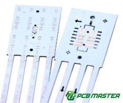
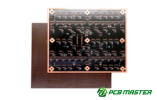
A Mini LED PCB is a type of printed circuit board (PCB) designed specifically to support Mini LED chips. These chips are much smaller than traditional LEDs, allowing for higher density and more precise control over light output. The Mini LED PCB provides the electrical connections needed to power the LEDs, as well as efficient paths for heat dissipation, which is critical for maintaining the performance of the LEDs.
The structure of a Mini LED PCB consists of several layers:
1. Mini LED Chips: These tiny, powerful light sources emit the brightness and color that drive the display.
2. Electrical Connections: Precision circuits are used to power each LED, ensuring that they receive the correct voltage and current.
3. Heat Management: Since LEDs can generate significant heat, Mini LED PCBs often incorporate heat dissipation elements, such as copper layers or even metal substrates, to prevent overheating and ensure longevity.
Role of Mini LED PCBs in Display Modules
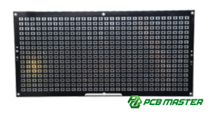
In display modules, Mini LED PCBs play an essential role in delivering superior visual performance. These PCBs serve as the foundation for Mini LED chips, positioning them in a grid-like arrangement to create vibrant, high-resolution displays.
For example, in 4K TVs, each pixel is made up of multiple Mini LEDs, and the PCB ensures that all these LEDs work together seamlessly. The PCB's design and materials allow for local dimming, where certain areas of the display can be darkened to create deeper blacks and higher contrast ratios. This makes Mini LED technology especially popular for applications requiring high-quality visuals, such as in gaming monitors or smartphones, where sharp contrast and vibrant colors are crucial.
In summary, the Mini LED PCB is a critical component that ensures the Mini LEDs function effectively, providing energy-efficient, high-quality light and contributing to the overall performance of advanced displays.
What Key Points Should Be Considered When Designing a Mini LED PCB?
When designing a Mini LED PCB, key points to consider include precise solder pad size and alignment, high-reflectivity solder mask, effective heat management with suitable materials, and strict control of flatness and warping to ensure reliable performance.
Solder Pad Design Considerations
Solder Pad Size and Precision Requirements
The size and spacing of the solder pads (typically 100-200μm) are critical to the proper functioning of Mini LED PCBs. These small pads must be precisely placed and sized to ensure reliable soldering of the Mini LED chips. Any deviation from the designed size or pitch (the distance between pads) can lead to poor solder joints, resulting in defects like misalignment, weak connections, or even complete failure of the display.
For example, if the pitch between the pads is too narrow, soldering errors like bridging (unintended connections between pads) are more likely to occur. A precise design ensures a clean, reliable connection between the Mini LEDs and the PCB, which is essential for maintaining the quality and longevity of the display.
Solder Pad Shape and Surface Treatment
There are two common types of solder pad designs: NSMD (Non-Solder Mask Defined) and SMD (Solder Mask Defined). NSMD pads are preferred for Mini LED PCBs because the solder mask window is slightly larger than the pad, allowing better solder attachment and reducing the risk of issues like lifted pads or insufficient solder joints.
In terms of surface treatment, ENIG (Electroless Nickel Immersion Gold) is the most recommended, as it provides a smooth, flat surface ideal for precise soldering and is resistant to oxidation. ENEPIG (Electroless Nickel Electroless Palladium Immersion Gold) offers even better performance but at a higher cost. Avoid HASL (Hot Air Solder Leveling) as it results in an uneven surface that can affect the precision of the Mini LED placement.
Solder Mask and White Ink Design Requirements
Solder Mask Ink Reflectivity and Color Requirements
For Mini LED PCBs, high-reflectivity white solder mask ink is essential, especially in areas between the Mini LEDs. The solder mask acts as a background and helps improve light efficiency by reflecting and diffusing light more evenly. A key standard for solder mask ink is a L-value (whiteness) of ≥92, which ensures a bright and uniform white appearance. Additionally, the ink should not show signs of yellowing or grayish tones over time, as this would negatively impact the display's brightness and contrast.
For instance, when manufacturing Mini LED backlit displays in high-end TVs, the reflectivity of the solder mask greatly influences how well the light from the LEDs is spread across the screen, contributing to better image quality.
Solder Mask Alignment and Ink Thickness Control
Alignment accuracy is critical when applying the solder mask. The mask’s opening for each solder pad must align precisely with the pad’s position, with a tolerance of ≤25μm. Misalignment could lead to issues such as exposed copper, which can cause short circuits or poor soldering.
Furthermore, ink thickness must be controlled to prevent defects like copper exposure or uneven soldering. Typically, two rounds of ink printing are necessary to achieve the required coverage and avoid problems like "dog teeth" (jagged edges) or inconsistent coatings.
Material Selection and Heat Management Considerations
The Impact of Material Selection on Thermal Management
The material choice for Mini LED PCBs is crucial for effective thermal management. Since Mini LEDs generate heat during operation, it’s important to use materials that can handle high temperatures without warping or degrading. High Tg materials like FR-4 High Tg and IT-180 are preferred because they can withstand temperatures above 170°C, preventing the PCB from deforming during reflow soldering or over time.
For instance, using a lower-quality material might lead to PCB warping after repeated heating and cooling cycles, compromising the performance of the LEDs.
Metal Core PCBs and Thermal Design
MCPCB (Metal Core PCB), typically made with aluminum, is often used in high-power Mini LED applications because of its excellent heat dissipation properties. Thick copper foil is another option for improving thermal conductivity. In these designs, thermal vias or heat sinks are often incorporated to move heat away from sensitive areas, ensuring that the LEDs don’t overheat.
When designing for efficient thermal management, conductive holes are used to route heat away from the LED chips to the back of the PCB, where it can be dissipated more effectively. These thermal vias should have a copper thickness ≥25μm to ensure optimal heat transfer.
Flatness and Warping Control Requirements
Warping Standards and Control
Warping is a major issue in Mini LED PCBs. Even a small amount of distortion can cause issues during assembly, leading to misalignment of LEDs or even vacuum leakage when applying suction to position the LEDs. The warping standard for Mini LED PCBs is generally ≤0.5%, but for large-sized PCBs, this value can drop to ≤0.3%.
To minimize warping, it’s important to control factors like material symmetry and layer compression. Proper material selection and precision in the manufacturing process are key to maintaining flatness.
Laminate Symmetry and Copper Distribution Importance
Laminate symmetry and balanced copper distribution are essential in preventing warping. Using a symmetric laminate stack-up and ensuring even copper layers throughout the PCB helps reduce stress during the lamination process, preventing uneven expansion or contraction that could lead to warping.
For example, an asymmetric stack-up, where one layer of the PCB has much thicker copper than others, can create internal stress, causing the board to bend or twist during the manufacturing process. Ensuring that copper is evenly distributed helps maintain the structural integrity of the Mini LED PCB.
How to Control Quality During Mini LED PCB Production?
Quality during Mini LED PCB production can be controlled by precisely managing etching, lamination, drilling, solder mask printing, and surface treatments, ensuring uniformity, accuracy, and adherence to strict standards.
Precision Requirements for Inner Layer Patterns and Etching
Line Width and Spacing Control Methods
In Mini LED PCB production, precise line width and spacing are critical for maintaining the integrity of the circuit design. High-precision photoplotters and Laser Direct Imaging (LDI) devices are commonly used to achieve this. These tools enable fine control over the photomask or the direct imaging of tiny traces on the PCB, ensuring that the line width and spacing meet strict specifications.
For instance, in high-performance applications such as Mini LED backlighting, any deviation in the trace width or spacing can lead to performance issues, such as weak electrical signals or shorts. By using these advanced technologies, manufacturers can achieve the required precision to support the small-scale circuitry of Mini LED PCBs.
Copper Thickness Uniformity Control
Maintaining uniform copper thickness is crucial for both electrical performance and thermal management. The etching solution used during PCB manufacturing needs to be carefully controlled to avoid non-uniform copper removal. Improper control can lead to uneven copper distribution, which can affect the efficiency of heat dissipation or electrical conductivity.
Manufacturers must constantly monitor etching solution parameters, such as temperature, concentration, and exposure time, to ensure that copper thickness is consistent across the entire board. Regular testing and inspections using techniques like cross-sectional analysis can verify the uniformity of copper layers and ensure reliable performance.
Quality Control During Lamination
Glue Flow and Lamination Parameter Control
During the lamination process, controlling the amount of glue flow is essential to prevent excess glue, which could lead to uneven surfaces or warped boards. The glue flow must be precisely regulated to ensure that it only fills the gaps between the PCB layers without overflowing onto the copper pads.
Additionally, the lamination parameters—such as temperature, pressure, and time—must be closely monitored to prevent defects like bubbles, delamination, or uneven compression. These issues can cause the layers to separate, affecting the structural integrity and performance of the Mini LED PCB. Ensuring consistent pressure and temperature during lamination helps maintain a smooth and stable board surface.
Precision Control for Drilling and Hole Metallization
Drilling Precision Requirements
Drilling precision is a key aspect of Mini LED PCB production. As the holes in the PCB need to be precisely aligned with the solder pads and vias, small-diameter drills are used to ensure accuracy. The goal is to achieve precise hole placement while maintaining smooth hole walls.
For example, in high-density Mini LED boards, even slight misalignment of the holes can lead to soldering issues or poor electrical connections. Using advanced laser drilling and CNC drilling techniques, manufacturers can achieve high accuracy, reducing the risk of defects during assembly.
Copper Thickness and Uniformity Control for Vias
The copper thickness inside the drilled holes (especially for thermal vias) is critical for proper heat management. The copper inside these vias helps transfer heat from the Mini LED chips to the PCB’s back layer, ensuring effective cooling.
Manufacturers must adhere to a standard copper thickness of ≥25μm for vias, particularly those designed for thermal management. X-ray inspection and cross-sectional analysis are commonly used to check the copper plating's uniformity and ensure that it meets the required standards. If the copper plating is inconsistent, it can negatively affect the thermal performance and reliability of the Mini LED PCB.
Solder Mask Printing Process Requirements
Printing Equipment and Process Parameter Optimization
The quality of solder mask printing directly impacts the final quality of the Mini LED PCB. High-mesh screens and automatic alignment systems are used to precisely apply the solder mask over the PCB. The high mesh count ensures that fine patterns can be printed accurately, especially for Mini LED designs with tight spacing between pads.
Automatic alignment systems are critical for ensuring that the solder mask openings align perfectly with the pads. This precision prevents problems such as copper exposure or solder bridging. Adjusting print speed and solder mask thickness during production helps to maintain the necessary quality for each board.
Curing and Baking Process Control
After printing, the solder mask ink must be cured properly to achieve maximum adhesion and durability. The curing process involves heating the board to a specific temperature for a set amount of time. Overheating can cause the ink to degrade, leading to discoloration (often referred to as “yellowing”) or poor adhesion. Conversely, insufficient curing can result in weak ink layers that may peel off.
To prevent these issues, manufacturers follow the solder mask supplier's recommended curing schedule and ensure that the temperature and time are carefully controlled. This helps maintain the integrity of the solder mask, preventing long-term performance issues like poor light reflection or soldering defects.
Surface Treatment Standards
ENIG Surface Treatment Nickel-Gold Thickness Requirements
The surface treatment of the PCB is essential for ensuring the reliability of solder joints and overall PCB performance. ENIG (Electroless Nickel Immersion Gold) is the most common surface finish for Mini LED PCBs because it provides a flat, highly conductive surface. The nickel layer typically has a thickness of 3-5μm, while the gold layer is usually 0.05-0.1μm.
Maintaining the correct nickel and gold thickness is critical to avoid defects like black pad issues, where the gold plating fails to bond correctly to the nickel. If the gold layer is too thin, it can expose the nickel, leading to poor soldering and an increased risk of cracks or failures in the solder joints.
Preventing "Black Pad" Phenomenon
To prevent the “black pad” phenomenon, where the gold layer is improperly applied and leads to poor solder joints, manufacturers must carefully monitor the surface treatment process. pH levels, temperature, and immersion time must be tightly controlled to avoid excessive corrosion of the nickel layer during the gold plating process. Regular visual inspections and X-ray checks help ensure the surface finish remains intact and free of defects that could impair soldering.
How to Inspect and Test a Mini LED PCB?
To inspect and test a Mini LED PCB, key steps include visual checks using AOI for defects, final inspection for solder mask and surface quality, and reliability tests such as thermal stress and reflow soldering simulations to ensure durability and performance.
Standards and Methods for Visual Inspection
AOI Inspection in the Production Process
AOI (Automated Optical Inspection) plays a crucial role in inspecting Mini LED PCBs during production. It uses high-resolution cameras to scan the board, detecting defects such as incorrect soldering, misalignment, or missing components.
Key inspection points for AOI include:
1. Solder pad quality: Ensures pads are properly formed and free from defects like excessive or insufficient solder.
2. Component placement: Verifies that Mini LEDs are correctly placed on the PCB and properly aligned.
3. Visual defects: Detects any visible surface issues like scratches, cracks, or discoloration that could affect performance.
AOI helps identify defects early in the production process, reducing the risk of more significant issues later on. By implementing AOI at multiple stages—such as after soldering or before assembly—manufacturers can ensure higher quality and reduce the need for rework.
Final Inspection and Quality Control
In the final inspection stage, manufacturers check critical features like white solder mask color uniformity and surface flatness to ensure the PCB meets the required standards.
l White solder mask color: The solder mask should have a high reflectivity and consistent whiteness to avoid uneven brightness and color issues in the final Mini LED display.
l Surface flatness: Any warping or distortion can affect the positioning of the Mini LEDs, leading to poor image quality. Final checks use tools like laser scanners to ensure the board's surface is flat within acceptable tolerances.
A thorough final inspection ensures that the Mini LED PCB is ready for integration into display modules, with no defects affecting functionality or aesthetics.
Reliability Testing and Soldering Performance Testing
Thermal Stress and Temperature Cycling Tests
To ensure the durability of Mini LED PCBs, thermal stress testing and temperature cycling tests are conducted. These tests simulate the extreme temperature changes the PCB might face in real-world applications.
l TCT (Thermal Cycling Test): The PCB is subjected to alternating high and low temperatures to test its ability to withstand thermal expansion and contraction. This simulates conditions such as sudden temperature changes in electronic devices.
l Thermal Shock Testing: The PCB is exposed to rapid temperature fluctuations to check for potential issues like cracks or delamination. These tests ensure that the PCB can endure thermal stresses without failure.
These tests are crucial to assess how the Mini LED PCB will perform under varying environmental conditions and ensure long-term reliability.
Reflow Soldering Simulation and Soldering Performance Evaluation
Reflow soldering is a key process in Mini LED PCB assembly. To ensure strong and reliable solder joints, manufacturers conduct reflow soldering simulations to evaluate the effectiveness of the soldering process.
Key soldering performance tests include:
l Solder joint integrity: Ensures that the solder joints between the Mini LEDs and the PCB are strong and electrically conductive.
l Wetting: Checks if the solder flows smoothly over the pad, creating a proper bond.
l Solder bridging: Detects unwanted connections between adjacent pads, which could cause electrical shorts.
By simulating the reflow process and assessing solder quality, manufacturers can identify potential issues like cold solder joints, poor wetting, or solder bridges, ensuring the final product meets strict performance standards.
What are the Performance Requirements and Optimization Directions for Mini LED PCBs?
Challenges and Solutions in Efficient Heat Dissipation Design
Importance of Thermal Path Design
Effective heat dissipation is one of the most critical factors for ensuring the reliable performance of Mini LED PCBs. These small LEDs generate significant heat, which can affect the quality and longevity of the display if not properly managed. Optimizing the thermal path—the route that heat takes from the LEDs to the PCB's back surface—is essential to prevent heat buildup.
To optimize the thermal path:
l Use high-conductivity materials such as aluminum or copper for the PCB substrate or MCPCB (Metal Core PCB) to quickly transfer heat away from the LEDs.
l Incorporate thermal vias or heat sinks to direct heat to areas of the PCB designed to dissipate it effectively.
l Increase copper thickness in the PCB's power and ground layers to enhance heat transfer.
Proper thermal management not only prevents overheating but also helps maintain the brightness and color stability of the Mini LEDs, which is essential for high-quality displays.
Strategies for Enhancing Display Quality
Balancing Brightness, Contrast, and Color
The quality of the Mini LED display depends on several factors, including brightness, contrast, and color accuracy. These factors must be carefully balanced to provide vivid images without overdriving the LEDs, which can lead to inefficiency or shortened lifespan.
To optimize these qualities:
l Reflectivity and uniformity of the white solder mask and solder mask ink are critical. Using high-reflectivity inks (L-value ≥ 92) ensures even light diffusion across the board, enhancing brightness and contrast.
l The solder mask's uniformity is equally important. Any variation in thickness or color can cause uneven lighting, leading to a poor viewing experience.
By optimizing the reflection and uniformity of materials like solder mask ink, manufacturers can improve both the visual appearance and the efficiency of the Mini LED display, resulting in clearer images with higher contrast and accurate color reproduction.
Key Factors for Extending Mini LED PCB Lifespan
Thermal Management and Material Selection for Longevity
The lifespan of a Mini LED PCB is directly influenced by the quality of its thermal management and material choices. Excessive heat is a major contributor to component degradation, so effective heat dissipation is essential for prolonging the life of the PCB.
To enhance lifespan:
l Use high-Tg (glass transition temperature) materials, such as FR-4 High Tg or IT-180, to prevent warping or delamination during high temperatures.
l Incorporate MCPCB designs with thermal vias to ensure that heat is efficiently transferred away from the LEDs, reducing the likelihood of thermal damage.
l Select materials with low CTE (Coefficient of Thermal Expansion), as they are better able to withstand the stress caused by thermal cycling (repeated heating and cooling).
By selecting appropriate materials and incorporating advanced thermal management solutions, manufacturers can significantly improve the durability and lifetime of Mini LED PCBs, ensuring consistent performance over time.
Conclusion
Achieving optimal performance in Mini LED PCBs requires careful attention to heat management, display quality, and long-term durability. By using advanced materials, precise manufacturing techniques, and effective thermal solutions, these challenges can be overcome, ensuring top-notch performance for Mini LED displays. At PCBMASTER, a trusted and experienced PCB and PCBA supplier, we are dedicated to delivering high-quality products, including Mini LED PCBs, to meet the ever-evolving demands of the display industry. Let us help bring your vision to life with precision-engineered solutions.
FAQs
1. How Does the Pad Design of a Mini LED PCB Affect Soldering Performance?
The pad design of a Mini LED PCB plays a crucial role in soldering performance, as it directly impacts the adhesion of the solder to the PCB. Accurate pad sizing and alignment are essential to ensure a strong and reliable connection between the Mini LED chips and the PCB. If the pad dimensions or pad-to-pad spacing are incorrect, it can lead to cold solder joints, poor electrical connections, or solder bridges. Additionally, the choice of pad shape—such as using NSMD (Non-Solder Mask Defined) pads—helps increase solderability, reducing the risk of soldering defects.
2. Why is Choosing High Tg Material Critical for Mini LED PCBs?
High Tg (glass transition temperature) materials are essential for Mini LED PCBs because they can withstand high temperatures without warping or delaminating. Mini LEDs often operate at high temperatures and undergo multiple reflow soldering processes. High Tg materials, such as FR-4 High Tg or IT-180, provide greater thermal stability, ensuring that the PCB maintains its structural integrity under these conditions. Using low Tg materials could lead to board deformation, affecting the performance and reliability of the Mini LED display.
3. What are the Standards for Warping in Mini LED PCBs?
The warping standard for Mini LED PCBs is much stricter compared to traditional PCBs. The typical warping limit for Mini LED boards is ≤ 0.5%, and for larger boards, this limit can even be reduced to ≤ 0.3%. Excessive warping can cause issues during the assembly process, such as vacuum suction leakage during pick-and-place, leading to misalignment, shifted components, or even displacement of the Mini LED chips. Therefore, maintaining low warping is critical for the assembly quality and overall reliability of the board.
4. How Can the Thermal Management Performance of a Mini LED PCB Be Ensured?
To ensure effective thermal management of Mini LED PCBs, several factors must be optimized:
1. Thermal vias: Incorporating copper-filled vias in the PCB design helps conduct heat from the LED chips to the backplane.
2. Material selection: Using materials with high thermal conductivity, such as MCPCB (Metal Core PCB), enhances heat dissipation.
3. Copper thickness: Using thicker copper layers in the PCB helps improve the overall heat dissipation efficiency, especially for high-power Mini LEDs.
4. Heat sinks: In some designs, external heat sinks or thermal pads are used to further enhance heat dissipation.
By carefully selecting the materials and optimizing the layout for heat conduction and dissipation, manufacturers can ensure that the Mini LED PCB performs reliably at high brightness levels without overheating.
5. What Reliability Tests are Performed on Mini LED PCBs?
Reliability testing of Mini LED PCBs typically includes:
1. Thermal Stress Testing: This simulates the PCB's response to extreme temperature variations through TCT (Thermal Cycling Test) and thermal shock testing, ensuring the PCB can withstand repeated heating and cooling without failure.
2. Soldering Performance Testing: Reflow soldering simulations are used to evaluate the solder joints between the Mini LEDs and the PCB, ensuring strong, durable connections.
3. Mechanical Stress Testing: The PCB is tested for its ability to withstand physical stress, including bending and vibration during the assembly process or in operational environments.
4. Long-Term Reliability: Tests like high-temperature storage and humidity testing assess the PCB's durability under prolonged exposure to harsh conditions.
These tests ensure that the Mini LED PCB will perform reliably throughout its lifespan, even in demanding environments.

