


AI PCB Design: How Artificial Intelligence is Revolutionizing Circuit Board Creation
AI PCB design is a new way of using artificial intelligence to improve the process of creating printed circuit boards (PCBs). A PCB is the backbone of almost every electronic device, connecting different components like chips, resistors, and capacitors. Traditionally, designing a PCB requires a lot of manual effort to place components, route connections, and test for errors. AI changes this by automating many of these tasks, making the process faster, more efficient, and less prone to mistakes.
AI in PCB design can learn from previous designs and suggest improvements, reducing human error and speeding up the design cycle. It can also predict the best way to arrange components on the board, ensuring the design works well in terms of size, power usage, and signal integrity. This shift is transforming the electronics industry by enabling companies to produce high-quality PCBs more quickly and at a lower cost. As a result, AI is playing a key role in creating smarter, more efficient electronics, from smartphones to advanced medical devices.
How Does AI Enhance PCB Design?
AI enhances PCB design by automating tasks like layout, routing, and schematic generation, improving accuracy, and reducing time and costs through optimization and error detection.
Automating Design Tasks
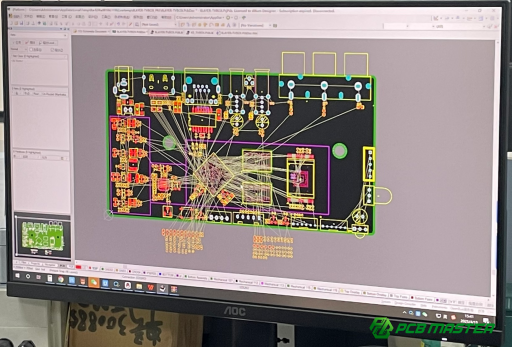
AI plays a crucial role in automating time-consuming tasks in PCB design, such as layout, routing, and schematic generation. Traditionally, engineers would manually place components on the board and route electrical connections, which is both slow and prone to errors. AI tools, however, can instantly analyze the design requirements and automatically suggest the best positions for components and the most efficient routing paths for signals. For example, software like Autodesk Eagle uses AI to automate layout suggestions, ensuring that the design is optimized for performance and space. This not only speeds up the design process but also makes it easier to handle complex designs, reducing human effort.
Improving Design Accuracy
AI significantly improves the accuracy of PCB designs by minimizing human error. When designing a PCB manually, even experienced engineers can make mistakes, especially when dealing with complex designs that involve many components. AI tools use machine learning algorithms that learn from past designs to detect potential errors or conflicts in real-time. For instance, AI can identify issues like component misplacement, improper signal routing, or power distribution problems. By catching these errors early, AI reduces the need for costly revisions and ensures that the design is more reliable and functional.
Reducing Time and Cost
The efficiency gains from using AI in PCB design are significant. By automating routine tasks like layout creation and routing, AI reduces the amount of time engineers spend on manual work. This leads to faster prototyping and quicker turnaround times for new products. Additionally, AI-driven design tools can optimize for cost-saving factors such as board size, material usage, and power efficiency. For example, AI can suggest design improvements that reduce the number of layers in a PCB, which not only cuts down manufacturing costs but also simplifies the production process. Ultimately, AI helps companies deliver high-quality products at a lower cost and in less time, giving them a competitive edge in the market.
Key AI Technologies in PCB Design
Key AI technologies in PCB design include machine learning for optimizing layout and routing, generative design for creating innovative alternatives, and predictive analytics for early error detection.
Machine Learning and Optimization
Machine learning algorithms in AI help optimize circuit board layout and routing by analyzing patterns in previous designs. These algorithms can identify the most efficient ways to place components and route signals, making the design process faster and more effective. For example, a PCB design tool like Altium Designer uses machine learning to learn from past designs, suggesting optimized routing paths that minimize signal interference and power loss. This reduces the manual effort required to find the best routing options and helps ensure the design is both functional and cost-effective. Machine learning continuously improves as it processes more data, leading to increasingly refined designs over time.
Generative Design
Generative design is an AI-driven process that creates innovative design alternatives based on specific parameters set by the engineer. Instead of manually designing a PCB, engineers can input constraints such as size, power requirements, and material preferences, and AI generates multiple design options that meet these criteria. The AI explores all possible solutions, often revealing unconventional yet optimal designs that a human engineer may not have considered. A real-life example of this is Autodesk Fusion 360, which uses generative design to create lightweight, highly efficient PCB layouts. This approach helps engineers explore a broader range of design possibilities, ensuring the final product is optimized for performance and cost.
Predictive Analytics for Error Detection
AI uses predictive analytics to detect and prevent design flaws early in the PCB development process. By analyzing past designs and their outcomes, AI can predict potential issues such as component misplacement, signal interference, or power problems before they arise. This allows engineers to make adjustments in real time, preventing costly errors during production. For example, AI-powered tools can automatically check for design rule checking (DRC) and alert the engineer about potential issues, such as insufficient spacing between traces. By catching these errors early, AI reduces the risk of design failures and helps ensure that the final PCB functions as intended, saving both time and money.
Benefits of AI in PCB Design
The benefits of AI in PCB design include faster prototyping, improved design quality with fewer errors, and enhanced customization for optimized performance.
Faster Prototyping and Reduced Time-to-Market
AI significantly speeds up the PCB design and prototyping process by automating time-consuming tasks such as layout creation, routing, and error checking. With AI-powered tools, engineers can quickly generate designs and make adjustments in real-time, which drastically shortens the design cycle. For example, AI-driven platforms like Altium Designer can automatically route connections and optimize component placement, reducing the time needed for manual adjustments. This allows companies to prototype faster and bring their products to market more quickly, giving them a competitive advantage. The faster the prototyping, the faster products can be tested and launched, which is crucial in industries like consumer electronics, where time-to-market is vital.
Better Quality and Fewer Errors
AI helps improve the quality of PCB designs by minimizing human errors, which are common in manual design processes. AI tools can automatically check designs for violations of design rules (DRC) and signal integrity issues, such as incorrect routing or improper component placement. By catching these errors early, AI reduces the need for costly revisions and ensures that the final design works as intended. For example, AI-powered simulation tools can predict how a PCB will behave under different conditions, helping to identify potential issues before the board is even produced. This leads to higher quality, more reliable PCBs with fewer defects, saving both time and money in the production phase.
Enhanced Customization and Performance
AI enables engineers to create highly customized PCB designs tailored to specific needs and performance requirements. By inputting constraints such as size, power, and material specifications, AI can generate multiple design alternatives that meet these unique parameters. This ensures that the final product is optimized for its intended purpose, whether it’s a compact mobile device or a high-performance computing board. For example, generative design tools like Autodesk Fusion 360 allow engineers to explore different configurations and select the one that delivers the best performance. With AI-driven solutions, companies can create PCBs that are more energy-efficient, cost-effective, and better suited for specific applications, leading to improved product performance and customer satisfaction.
Challenges in Adopting AI for PCB Design
The challenges in adopting AI for PCB design include integrating AI tools into existing workflows and the high cost and limited accessibility of advanced AI-powered design software.
Integration with Existing Workflows
One of the main challenges in adopting AI for PCB design is integrating AI tools into existing design workflows. Many companies still rely on traditional, manual methods for designing PCBs, and switching to AI-powered systems requires changes in how engineers approach their work. AI tools often come with a learning curve and require engineers to adapt to new interfaces and design processes. For example, when adopting AI tools like Altium Designer or Autodesk Eagle, engineers may need to learn how to use automation features for routing and layout optimization, which could disrupt their established workflow. Additionally, AI tools need to work seamlessly with existing software and hardware to avoid creating compatibility issues. Successfully integrating AI tools into a traditional PCB design process may require training, process adjustments, and a period of trial and error, which can slow down the adoption process.
Cost and Accessibility of AI Tools
Another challenge is the cost and accessibility of AI-powered PCB design tools. While AI offers significant advantages, many of the more advanced tools can be expensive, especially for small and medium-sized businesses. For example, high-end PCB design software with AI features can cost thousands of dollars annually for a single license, making it difficult for smaller companies to justify the investment. In addition to the initial costs, ongoing training and support may also add to the expense. On the other hand, some companies may struggle to find affordable AI tools that offer the necessary features for their specific needs. While there are some budget-friendly options on the market, they may not provide the full range of AI capabilities that larger companies require. As the AI market for PCB design grows, it is likely that more affordable and accessible tools will become available, but for now, cost remains a significant barrier for many.
Getting Started with AI PCB Design
To get started with AI PCB design, choose the right AI tool based on features, cost, and support, then gradually integrate AI into your workflow by automating tasks like routing, layout, and optimization.
Choosing the Right AI Tools
When selecting AI design software for PCB design, it’s important to consider a few key factors. First, assess the software’s features and whether it fits the specific needs of your project. Look for AI-powered tools that offer automated layout and routing, error detection, and optimization features. Popular tools like Altium Designer and Autodesk Eagle are known for their AI-driven capabilities, but you’ll need to compare them based on factors like ease of use, cost, and support. It’s also important to check if the software integrates with your existing workflow or other design tools you’re currently using. Another factor is the level of support and community resources available for the software. For beginners, it’s a good idea to choose a tool with good tutorials, documentation, and a strong user community. Finally, consider the cost of the software, as more advanced AI features can be expensive. Balancing features, support, and cost will help you choose the best AI tool for your needs.
Simple Steps to Implement AI in Your Design
Integrating AI into your PCB design workflow can be easy if you follow a few simple steps. Start by familiarizing yourself with the basic features of your chosen AI tool. Many tools offer tutorials or beginner guides, which are a great way to learn the basics. Next, begin by automating simple tasks, like component placement and routing, to get comfortable with how the AI operates. As you gain experience, gradually explore more advanced features like AI-driven error detection and optimization suggestions. For example, in Autodesk Eagle, you can start by using the AI-powered routing function, then expand to using machine learning to optimize component placement. It’s also a good idea to experiment with generative design features that allow the AI to suggest multiple layout options. As you integrate AI, make sure to continually test and validate your designs to ensure that the AI’s suggestions meet your performance and cost requirements. Over time, you will become more comfortable and efficient at using AI in your PCB design process.
The Future of AI in PCB Design
The future of AI in PCB design includes fully autonomous design processes and enhanced sustainability, with AI optimizing materials, energy usage, and design efficiency.
Autonomous PCB Design
In the future, AI could lead to fully automated PCB design processes, where human intervention is minimal or even unnecessary. Currently, AI assists engineers by automating certain tasks like routing and layout optimization, but future advancements could push this even further. With autonomous PCB design, AI could analyze a project’s requirements, generate the entire design, and make decisions about component placement, routing, and other crucial factors—all on its own. This would allow for the creation of high-quality, optimized PCBs in a fraction of the time it currently takes. Some companies are already exploring AI-driven automation for their hardware designs, and it’s likely that this technology will soon be more accessible to a broader range of businesses. Autonomous AI systems will be able to continually learn from past designs, improving with each new project, and making the PCB design process faster, more accurate, and more efficient.
AI and Sustainability
AI has the potential to make PCB design more eco-friendly and efficient, helping reduce the environmental impact of electronics production. One way AI can contribute to sustainability is by optimizing PCB designs to use fewer materials, reducing waste and the overall environmental footprint. AI-driven tools can analyze how to best lay out components on a board, allowing for smaller, more compact designs that require less raw material. Furthermore, AI can help optimize energy efficiency, ensuring that the design uses power in the most efficient way possible. For example, AI algorithms can reduce power consumption by optimizing routing to minimize signal interference, leading to lower energy requirements. Additionally, AI can help in selecting environmentally friendly materials by analyzing their performance and environmental impact. As sustainability becomes a higher priority in the electronics industry, AI will play a crucial role in creating greener, more efficient designs, contributing to a more eco-conscious future for PCB manufacturing.
Conclusion
As AI continues to shape the future of PCB design, it promises faster, more efficient, and eco-friendly solutions that will redefine how electronics are created. With advancements in automation, error detection, and optimization, engineers and companies can now look forward to streamlined workflows, reduced costs, and enhanced design accuracy. This transformation opens new doors for innovation in the electronics industry.
For businesses looking to stay ahead in this rapidly evolving field, partnering with experienced PCB and PCBA suppliers is crucial. Companies like PCBMASTER, with their deep expertise and commitment to quality, are already embracing AI technologies to offer top-tier PCB solutions. With years of experience in the industry, PCBMASTER ensures high-performance, reliable, and customized PCB and PCBA products that meet the latest design standards, making them a valuable ally for companies looking to innovate and grow in the digital age.
FAQs
How does AI speed up the PCB design process?
AI speeds up the PCB design process by automating several time-consuming and repetitive tasks. Tasks such as component placement, routing of signals, and even error detection can be handled by AI, allowing designers to focus on more complex aspects of the design, like optimizing performance or dealing with special requirements. AI tools can automatically suggest the best routing paths, helping engineers avoid manual trial-and-error processes. Additionally, AI can streamline the verification process by instantly checking designs for potential issues, cutting down the need for time-consuming reviews. This leads to quicker iterations and faster prototyping, reducing the overall design cycle and time-to-market.
Can AI completely replace human designers?
No, AI cannot completely replace human designers. While AI tools are powerful for automating routine tasks, human designers are still essential for making decisions that require creativity, complex problem-solving, and domain-specific knowledge. Designers bring a level of intuition, experience, and strategic thinking that AI currently cannot replicate. For example, engineers need to assess the performance of a design in real-world applications, make adjustments based on user feedback, and innovate in ways that AI can't predict or adapt to. AI complements designers by handling repetitive tasks, but the human touch remains crucial for making final design choices and handling unique design challenges.
What are the main challenges in using AI for PCB design?
There are several challenges in adopting AI for PCB design. First, integration with existing workflows can be difficult, as many companies still rely on traditional tools and processes that don’t easily align with AI-driven solutions. Engineers may need to learn new software, which requires training and adaptation. Costs can also be a barrier, as AI-powered design tools can be expensive, especially for small businesses. Some of the more advanced AI tools come with a high price tag, which might not be affordable for every company. Finally, specialized knowledge is required to fully leverage AI tools. Engineers may need to become familiar with machine learning, AI concepts, and specific software tools to make the most out of the technology, which can be a steep learning curve for those unfamiliar with AI.
What are the benefits of using AI in PCB design?
AI offers numerous benefits in PCB design, starting with improved design accuracy. AI-driven tools can detect errors such as incorrect routing or component placement before they become costly problems, helping to reduce design flaws. Fewer errors mean fewer revisions and faster iteration times. AI can also accelerate the design cycle by automating time-consuming tasks and suggesting optimal layouts or routing paths, which leads to faster prototyping and quicker product launches. Additionally, AI can optimize performance, for example, by suggesting ways to minimize power consumption or improve signal integrity, which enhances the overall quality of the PCB. The end result is a more efficient design process that saves both time and money.
Are AI-powered PCB design tools expensive?
The cost of AI-powered PCB design tools can vary widely. Some tools, especially those tailored for small businesses or entry-level designers, can be quite affordable and offer essential AI functionalities such as automated routing or component placement. Examples of such tools include simpler versions of software like Autodesk Eagle or KiCad that incorporate some AI features at a lower price. However, more advanced AI-powered tools, like Altium Designer, which offer comprehensive AI-driven automation and optimization features, tend to be more expensive. These high-end tools are often priced higher due to the advanced features they offer, making them more suitable for larger companies with complex design needs. The investment in AI tools is generally considered worthwhile for companies that require more robust design capabilities and need to reduce production times, though the cost may be a barrier for smaller businesses or startups.

