







How to Identify and Solve HDI PCB Issues: Drilling, Etching, and Reliability Tips
High-Density Interconnect (HDI) PCBs are at the heart of modern electronics, powering everything from smartphones to advanced industrial systems. Their compact design and fine circuitry deliver unmatched performance, but manufacturing them comes with a unique set of challenges. Small deviations during drilling, plating, or layering can escalate into significant reliability issues, impacting both functionality and product lifespan. Understanding these potential pitfalls is crucial for designers, engineers, and manufacturers striving for flawless HDI production.
PCBMASTER, with years of experience in high-precision PCB manufacturing , has observed recurring problem areas that can affect yield, signal integrity, and long-term reliability. By identifying the most common issues early—ranging from microvia defects to material stress failures—we can provide actionable insights and practical solutions to optimize every stage of HDI board fabrication. This guide dives into these challenges, offering structured analysis, expert recommendations, and testing strategies to ensure your HDI boards meet the highest standards.
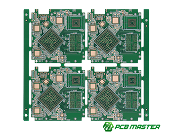
What are the most common microvia processing problems in HDI PCB production?
Microvias are small holes that connect layers in HDI boards. While they enable high-density designs, microvias are prone to defects that affect electrical performance and reliability. Common problems include laser drilling defects and issues during copper plating. Understanding these problems helps manufacturers improve yields and ensure long-term reliability. PCBMASTER uses high-precision processes and testing strategies to prevent these issues and optimize microvia quality.
Analysis of Laser Drilling Defects
Blind Via Misalignment: Causes and PCBMASTER Solutions
Blind vias sometimes shift from their intended positions due to small errors in alignment between the drill and the PCB layers. This misalignment can disrupt layer-to-layer connections, causing short circuits or signal loss. PCBMASTER addresses this problem using high-precision LDI (Laser Direct Imaging) systems that accurately align the board pattern before drilling. For example, a 40μm tolerance ensures proper electrical connection even on high-density boards.
Irregular Via Shapes: Cones and Bell Shapes
Laser-drilled vias may form cone-shaped or bell-shaped holes when laser energy or focus is not properly controlled. These shapes can reduce plating efficiency and weaken the copper lining. PCBMASTER optimizes laser energy and focal distance, adjusting for material thickness to create consistent, vertical hole walls that improve plating and reliability.
Resin Smear (Residue) Management
After drilling, some resin may remain on the hole walls, called “smear,” which reduces copper adhesion during plating. PCBMASTER uses chemical cleaning or plasma etching to remove this residue. Chemical cleaning dissolves resin evenly, while plasma etching provides a precise surface treatment without affecting the board structure.
Copper Nodules (Nodding) Formation
Copper nodules appear when the bottom layer copper is not fully vaporized during laser drilling. These small protrusions can block plating and cause shorts. PCBMASTER resolves this by adjusting laser power and speed, ensuring complete copper removal without damaging surrounding material.
Filling and Plating Issues and Optimization Solutions
Voids Formation: Causes and Solutions
Voids, or empty spaces inside plated vias, occur when gas is trapped or plating is incomplete. These can cause electrical failures under stress. PCBMASTER optimizes plating bath parameters, temperature, and agitation to allow copper to fully fill the vias. For example, introducing mild vibration during plating reduces trapped air and improves uniformity.
Via Dimple Problem: Impact on Lamination
Dimples form when the via top sinks below the board surface, usually over 20μm. They cause uneven lamination and may affect soldering. PCBMASTER controls plating thickness and performs pre-lamination inspections to minimize dimples. If detected, the board can be reworked or adjusted to maintain flatness.
Uneven Copper Thickness Inside Vias
Insufficient copper thickness inside vias (<10–15μm) reduces current-carrying capacity and reliability. PCBMASTER specifies minimum copper thickness and uses cross-section testing to ensure compliance. For instance, measuring via copper in sample boards ensures that plating is uniform before full-scale production.
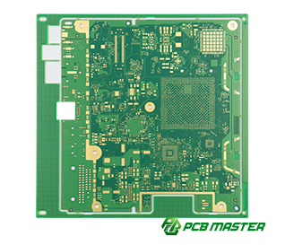
How to solve common lamination and alignment problems in HDI PCB production?
Lamination and alignment are critical steps in HDI PCB production. Misalignment between layers or incomplete lamination can lead to electrical failures, poor reliability, and board warping. Controlling materials, process parameters, and temperature profiles is key to avoiding these issues. PCBMASTER leverages precision equipment and process expertise to maintain accurate layer registration and prevent delamination.
Misregistration Problems Between Layers
Core and Prepreg Material Expansion Differences
Misregistration occurs when the core board and prepreg (PP) layer expand or shrink differently during lamination. This happens because materials have different thermal expansion properties (CTE) and glass transition temperatures (Tg) . For example, a core may expand slightly more than the prepreg under heat, shifting via positions. PCBMASTER manages this by selecting materials with compatible Tg/CTE values and by controlling the lamination temperature and pressure profile carefully. This minimizes layer-to-layer misalignment.
Cumulative Offset from Multiple Pressing Steps
HDI boards often require multiple lamination steps. Each step can add a small offset, which accumulates and may misalign high-density vias. For advanced HDI boards, the total misalignment must stay ≤25μm. PCBMASTER uses precision alignment tools and stage-by-stage verification to ensure cumulative errors do not exceed this tolerance.
PCBMASTER Recommended Lamination and Alignment Practices
PCBMASTER recommends a controlled lamination process: preheating layers evenly, using high-precision vacuum presses, and checking registration at each stage. Real-time optical inspection ensures alignment errors are caught early, reducing rework and improving yield.
Common Causes of Delamination and Board Splitting
Insufficient Resin Filling
Delamination often occurs when the prepreg resin does not fully fill the gaps between layers. This leaves weak interfaces that can separate under stress. PCBMASTER monitors resin flow during lamination and selects prepreg with appropriate resin content for high-density designs.
Z-Axis Expansion During High-Temperature Reflow
During lead-free reflow soldering, boards expand in the Z-axis (thickness), which can stress the lamination and cause layer separation or “board splitting.” PCBMASTER mitigates this by using high-Tg materials and controlling reflow temperature ramps to limit vertical expansion.
Special Considerations for Halogen-Free Materials
Halogen-free prepregs often have lower flowability, increasing the risk of delamination. PCBMASTER adjusts lamination pressure, temperature, and dwell time to ensure full resin flow and strong layer adhesion, even with environmentally friendly materials.
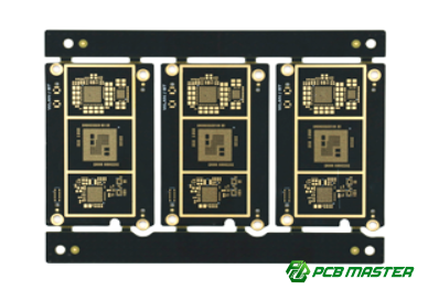
What are the common fine-line defects in HDI boards and how can they be improved?
Fine-line defects in HDI PCBs can reduce electrical performance, cause short circuits, and lower manufacturing yield. These defects usually occur during etching, patterning, or surface treatment. By understanding the causes and using proper process control, manufacturers can ensure precise, reliable circuitry. PCBMASTER applies optimized etching, exposure, and copper surface treatment methods to prevent these common issues.
Fine-Line Etching Problems
Under-Etching or Over-Etching and Line Width Tolerance Control
Under-etching leaves extra copper, while over-etching removes too much, causing narrow or broken traces. For example, a 3mil line may shrink below 2.5mil if over-etched, reducing current capacity. PCBMASTER manages line-width tolerance by carefully controlling etchant concentration, temperature, and etch time. Optical inspections verify that the lines meet design specifications before proceeding.
Thin Copper and Corner Loss
Copper tends to be thinner at trace corners due to uneven etching or plating, which can reduce conductivity and reliability. PCBMASTER minimizes corner loss by adjusting copper deposition and optimizing etch pattern design, ensuring consistent thickness even on sharp bends.
Rough Edges (Roughness) and Exposure/Development Optimization
Rough or jagged edges on fine lines occur when photoresist exposure or development is inconsistent. This can increase impedance and create soldering defects. PCBMASTER improves line smoothness by using high-resolution photoresists, precise LDI exposure, and controlled development times. Smooth edges improve signal integrity and solderability.
Copper Surface Treatment Defects and Prevention
ENIG/OSP Surface Treatment Unevenness and Soldering Issues
Uneven ENIG (Electroless Nickel Immersion Gold) or OSP (Organic Solderability Preservative) layers can lead to poor solder wetting, cold joints, or component failures. PCBMASTER prevents this by controlling plating thickness, monitoring bath chemistry, and performing surface inspections to ensure uniform coverage across the PCB.
Black Pad Risk and PCBMASTER Quality Control
“Black Pad” refers to a thin, corroded nickel layer under the gold, which weakens solder joints. It occurs when nickel plating is over-processed or chemically attacked. PCBMASTER reduces this risk by maintaining strict nickel bath control, limiting exposure to contaminants, and conducting cross-section inspections to verify surface quality before assembly.
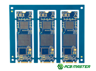
What are the main material challenges in HDI PCB manufacturing?
HDI PCBs often use specialized materials to achieve high-speed signal performance and reliability. However, these materials introduce challenges in lamination, layer thickness control, and thermal stress. Selecting compatible materials and managing process parameters is critical to prevent delamination, cracking, and signal degradation. PCBMASTER applies precise material selection and process monitoring to overcome these challenges.
High-Frequency Material Compatibility Issues
Adjusting Lamination Parameters for Low Dk/Df Materials
Low dielectric constant (Dk) and low dissipation factor (Df) materials, like Panasonic Megtron or Rogers substrates, are commonly used in HDI boards for high-speed signals. These materials require precise lamination settings because they react differently to heat and pressure compared to standard FR-4. PCBMASTER adjusts temperature, pressure, and dwell time during lamination to avoid resin flow problems or voids, ensuring signal integrity for high-frequency applications.
Controlling Dielectric Layer Thickness After Multiple Laminations
HDI boards often undergo multiple lamination steps. Each step can slightly change the thickness of dielectric layers, which can affect impedance and signal performance. PCBMASTER monitors each layer using thickness measurement tools and adjusts lamination conditions to keep dielectric thickness within ±8% of the design target. This ensures consistent electrical performance across high-density boards.
Thermal Stress and Reliability Failures
Via Cracking Due to CTE Mismatch
A common reliability issue is via cracking, caused by mismatch in the coefficient of thermal expansion (CTE) between copper and the substrate. When the board heats up during soldering or operation, uneven expansion can stress the vias and cause cracks. PCBMASTER minimizes this risk by selecting materials with compatible CTE and controlling thermal profiles during reflow and other thermal processes.
Preventing Base Material Delamination at Lead-Free Soldering Temperatures
Lead-free soldering requires higher temperatures (~260°C), which can cause delamination in some HDI substrates if the resin cannot withstand heat. PCBMASTER uses high-Tg materials and optimizes preheating, ramp-up, and cooling rates during reflow to prevent layer separation while maintaining mechanical stability and reliability.
What are the common testing and reliability issues in HDI PCB manufacturing?
HDI PCBs contain microvias, blind vias, and buried vias, making testing and reliability evaluation more complex than standard PCBs. Undetected defects can lead to short circuits, open circuits, or long-term failures. Effective testing strategies and reliability analyses are essential to ensure board quality. PCBMASTER combines advanced non-contact testing, accelerated reliability tests, and microscopic analysis to detect hidden issues and prevent failures.
Blind and Buried Via Testing Challenges
Non-Contact Testing and Increasing Test Points
Blind and buried vias are difficult to test electrically because they are not accessible from the board surface. Non-contact testing methods, such as automated optical inspection (AOI) and X-ray imaging, can detect via connectivity and hidden defects. PCBMASTER also recommends adding test points in the design stage to improve test coverage, ensuring even microvias deep inside the board are evaluated without destructive methods.
Detecting Micro Short Circuits and Micro Open Circuits with Four-Wire Testing
Micro short circuits and tiny open circuits (<10MΩ) are easy to miss using standard two-probe testing. PCBMASTER uses four-wire (Kelvin) testing, which reduces measurement errors caused by probe resistance and detects weak connections accurately. This method ensures that subtle electrical failures in HDI boards are caught early, improving product reliability.
CAF (Conductive Anodic Filament) Risk and Testing Methods
Analyzing Ion Migration in High-Humidity Environments
CAF occurs when ions migrate between layers under moisture and voltage, creating conductive filaments that cause shorts. This risk increases when via spacing is less than 150μm. PCBMASTER evaluates CAF susceptibility by simulating high-humidity conditions, monitoring for early signs of filament formation, and adjusting materials or design spacing to prevent failures.
PCBMASTER Accelerated CAF Testing Process
PCBMASTER uses an accelerated CAF test with conditions of 85°C/85% relative humidity and a 5–10V bias for 500 hours. This method quickly identifies boards prone to CAF failures, allowing design or process adjustments before mass production. It follows IPC-650 standards to ensure consistency and reliability.
Specialized Failure Analysis Testing Recommendations
Electromigration Testing
Electromigration occurs when high current density moves metal atoms in a via or trace, potentially causing open circuits. PCBMASTER performs accelerated electromigration tests by cycling high currents and monitoring resistance changes. This identifies weak points in the design or plating process.
Cross-Section Analysis
Microscopic cross-sectioning allows measurement of via copper thickness, void ratio, and interface cracks. PCBMASTER uses this method to verify plating uniformity (target ≥15μm), ensure filling voids are below 5%, and detect interface cracks less than 5μm. These measurements confirm structural integrity and long-term reliability of HDI boards.
How can HDI PCB design and manufacturing collaboration issues be avoided?
Effective collaboration between design and manufacturing is essential for HDI boards, which have dense circuitry, multiple layers, and fine vias. Poor design decisions can cause lamination warping, via cracking, and overheating in high-density areas. PCBMASTER helps designers anticipate manufacturing challenges and optimize layouts to improve yield, reliability, and thermal performance.
Warping Caused by Non-Standard Laminate Structures
Risks of Asymmetric Laminate Structures
Non-standard or asymmetric layer stacking can cause uneven stress during lamination, leading to board warping. For example, a thicker copper layer on one side compared to the other creates mechanical imbalance when heated, bending the PCB. PCBMASTER advises keeping symmetrical stacking whenever possible and balancing copper distribution across layers to reduce warping risks.
PCBMASTER Recommended Design Optimization
To prevent warping, PCBMASTER suggests simulating layer expansion during design, adjusting layer thickness, and standardizing core-to-prepreg ratios. These steps help ensure mechanical stability after lamination and improve yield in high-density HDI boards.
Stacked Via Cracking
Mechanical Stress Concentration Causes
Stacked blind vias can crack because mechanical stress concentrates at the via interface, especially when vias are tall or plated unevenly. Thermal cycling during soldering or operation can worsen these cracks. PCBMASTER reduces this risk by recommending staggered via designs, optimized via diameter, and proper plating to distribute stress evenly.
Local Overheating and Design Improvements
High-Density Area Overheating Risks
In high-density regions with many components or vias, heat can accumulate, causing localized thermal stress. Overheating can reduce reliability, accelerate CAF formation, and damage components. PCBMASTER identifies high-density zones during design review and applies thermal simulation to predict hotspots.
Thermal Via Design and Heat Management Optimization
Thermal vias or heat-spreading planes are inserted in dense areas to conduct heat away from critical components. PCBMASTER optimizes via placement, size, and copper thickness to improve thermal dissipation. This reduces hot spots, enhances reliability, and supports high-speed signal integrity.
Conclusion
High-Density Interconnect (HDI) PCBs bring high performance in compact sizes, powering everything from smartphones to industrial systems. However, their dense layouts and fine features make them more sensitive to manufacturing and reliability challenges, such as microvia defects, layer misalignment, copper plating issues, and thermal stress.
PCBMASTER’s approach focuses on careful design, precise process control, and thorough testing. By addressing common problems—like misregistration, CAF formation, or surface treatment inconsistencies—early in production, engineers can improve board quality, yield, and long-term reliability.
From optimizing laser drilling and lamination to controlling material behavior and heat management, each step matters. With experience and proper planning, designers and manufacturers can produce HDI PCBs that perform reliably in demanding applications, ensuring high signal integrity and stable operation over time.
FAQs
1. How can large deviations in HDI microvia drilling be resolved?
Large microvia deviations occur due to misalignment or improper laser settings. The solution is to use high-precision LDI (Laser Direct Imaging) systems for accurate positioning, carefully control laser energy and focus, and perform real-time inspection during drilling. Proper maintenance of equipment and calibration also reduces positional errors and improves layer interconnection reliability.
2. How can over-etching or under-etching of fine lines be effectively prevented?
Over- or under-etching happens when etch time, temperature, or chemical concentration is not well controlled. To avoid this, monitor etchant parameters closely, use high-resolution photoresist, and apply optical inspection after etching. Adjusting the process to maintain line-width tolerance ensures copper traces remain within design specifications, avoiding shorts or weak conductivity.
3. How can dielectric layer thickness variation be controlled after multiple laminations with high-frequency materials?
Dielectric thickness can change due to pressure and temperature effects in each lamination step. To control this, measure layer thickness at each stage, adjust lamination pressure, temperature, and dwell time, and use materials with stable Tg and compatible CTE. Consistent monitoring ensures thickness stays within ±8% of design targets, maintaining signal integrity.
4. How can electrical testing of blind and buried vias be improved?
Blind and buried vias are hard to access electrically. Solutions include adding extra test points in the design and using non-contact methods such as X-ray inspection or AOI. Micro short and open circuits can be detected using four-wire (Kelvin) testing, which accurately measures low-resistance or weak connections without probe errors.
5. How can CAF (Conductive Anodic Filament) risk be reduced through design and testing?
CAF forms when ions migrate between layers under humidity and voltage. To reduce risk, increase via spacing where possible, select compatible materials, and optimize lamination. Accelerated CAF testing under 85°C/85% RH with a bias voltage for 500 hours helps identify vulnerable boards early. Monitoring high-density areas and using proper plating processes also prevents CAF formation.
About the Author

Carol Luo
PCB Design EngineerI'm Carol, a PCB Engineer at PCBMASTER with experience in PCB design and manufacturing engineering since 2018. I focus on translating engineering requirements into reliable PCB solutions, with expertise in stack-up design, material selection, and design-for-manufacturing (DFM). I share practical engineering insights from real-world PCB design and production experience.
Visit Carol Luo's Profile