


Flexible PCB Assembly Techniques to Boost Reliability and Performance
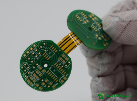
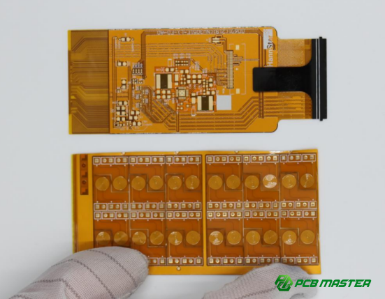
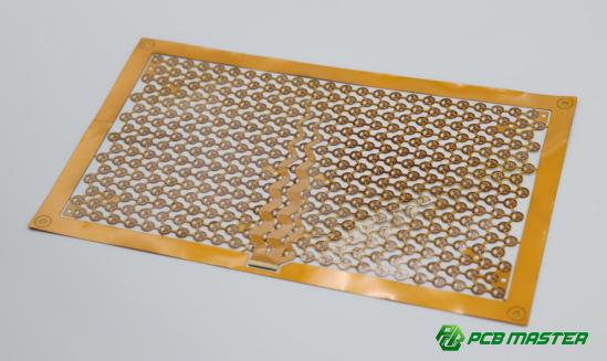
Flexible PCBs, also called FPCs, are thin, bendable circuit boards that allow electronics to fit into compact, irregular shapes. They are widely used in modern devices like smartphones, wearables, medical instruments, and automotive systems because they save space, reduce weight, and improve durability. Unlike rigid boards, flexible PCBs can bend, twist, and fold without breaking, making them essential for high-performance electronics that demand reliability in small or moving spaces.
As an experienced PCB and PCBA supplier, PCBMASTER ensures high reliability and optimal performance through advanced flexible PCB assembly techniques. Our processes focus on precise component placement, controlled soldering, and stress-reducing strategies that prevent defects like broken traces or poor solder joints. By carefully managing assembly parameters and using specialized equipment, we improve signal integrity, mechanical stability, and overall device lifespan.
This article focuses exclusively on flexible PCB assembly methods and performance optimization. It does not cover general PCB design principles or unrelated electronics topics. Instead, readers will gain practical insights into assembly techniques, testing procedures, and quality assurance strategies that directly enhance reliability and performance in real-world applications. Examples and case studies demonstrate how proper assembly choices lead to durable, high-performing flexible PCBs that meet modern electronics demands.
What Are the Key Flexible PCB Assembly Techniques for Enhanced Reliability?
Flexible PCB assembly techniques are essential for improving the durability and performance of bendable circuits. The most effective methods include:
l Surface Mount Technology (SMT): Lightweight, compact component placement.
l Through-Hole Technology (THT): Strong mechanical support for heavy components.
Adhesives and Stiffeners: Reduce mechanical stress and improve long-term reliability.
Each technique addresses challenges such as mechanical stress, heat sensitivity, and solder joint durability. Correct implementation ensures flexible PCBs can bend, twist, and operate reliably over long periods in modern electronic devices.
Surface Mount Technology (SMT) in Flexible PCB Assembly
SMT can be adapted for flexible PCBs, but special care is required due to the board’s thin, heat-sensitive nature. Key considerations include:
l Board Warping: Controlled reflow oven temperatures and support carriers prevent bending.
l Component Placement Accuracy: Precise pick-and-place machines ensure correct alignment.
l Soldering Quality: Proper reflow profiles avoid cold joints and misalignment.
Step-by-step SMT assembly process on a flex PCB:
1. Apply solder paste to the PCB pads.
2. Place components with a pick-and-place machine.
3. Reflow solder under controlled temperature to avoid warping.
4. Inspect for alignment and solder quality using optical inspection.
Following this workflow ensures strong solder joints and reliable electrical connections even on flexible circuits.
Through-Hole Technology (THT) Considerations for Flex PCBs
THT offers strong mechanical support but requires adaptation for flexible PCBs:
l Differences from rigid PCBs: Bending stress can crack solder joints; careful soldering temperature and lead length control are necessary.
l Reliability factors: Joint durability and stress resistance are key for long-term performance.
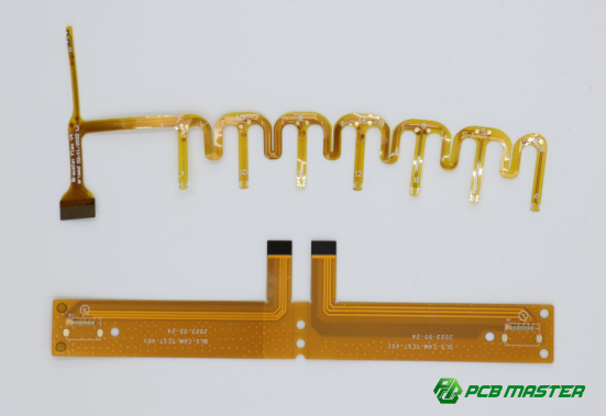
l Hybrid designs: Place THT components on rigid sections, leaving flexible zones for SMT components.
Example: In wearable devices, THT components support heavy connectors on rigid areas, while flexible zones allow bending around small casings. This ensures both mechanical stability and device flexibility.
Advanced Adhesive and Stiffener Techniques
Adhesives and stiffeners enhance stability and reduce stress in flexible PCBs:
l Adhesives: Secure components during handling and soldering, reducing movement and potential defects.
l Stiffeners: Strategically placed under heavy components or along bends to reduce mechanical stress.
l Benefits: Protect solder joints, prevent trace damage, and improve long-term reliability.
Practical example: Foldable smartphones and wearable devices often use stiffeners under connectors and key components, ensuring the flexible PCB can endure repeated bending without performance loss.
How Can Flexible PCB Assembly Improve Electrical Performance?
Flexible PCB assembly can significantly enhance electrical performance by ensuring proper signal flow, reducing defects, and minimizing stress on components. Key techniques include optimizing trace routing, using precise soldering methods, and carefully selecting and placing components. Applying these methods improves signal integrity, reduces electrical failures, and ensures reliable operation in high-frequency and compact applications.
Optimizing Trace Routing for Signal Integrity
Proper trace routing is critical to maintaining signal quality on flexible PCBs. Key strategies include:
l Controlled Impedance: Ensures signals travel without distortion, important for high-speed electronics.
l Trace Width and Spacing: Wider traces carry more current; proper spacing prevents crosstalk between signals.
l Differential Pairs Example: Placing two complementary signals close together reduces noise and improves high-frequency performance.
For instance, in a wearable health device, carefully routed differential signal pairs allow accurate data transmission from sensors to the main processor, even when the board bends. Optimizing trace routing prevents signal loss and ensures reliable device operation.
Soldering Techniques to Minimize Electrical Failures
Correct soldering is essential for flexible PCB performance. Considerations include:
l Lead-Free vs. Leaded Solder: Lead-free is environmentally friendly but requires precise temperature control; leaded solder melts at lower temperatures, reducing stress on flex boards.
l Reflow Profile Optimization: Adjusting heating and cooling rates prevents warping and ensures uniform solder joints.
l Avoiding Common Defects: Techniques such as controlled solder paste application prevent tombstoning, cold joints, and bridging.
For example, PCBMASTER optimizes reflow profiles for each flex PCB type, ensuring that solder joints are strong and reliable even under repeated bending in portable electronics.
Component Selection and Placement Strategies
Choosing and placing the right components directly impacts electrical performance:
l Component Criteria: Size, weight, and flexibility are critical; lightweight, compact components reduce stress and prevent trace damage.
l Placement Orientation: Aligning components with the natural bending direction reduces mechanical stress and preserves signal integrity.
A practical case is in foldable smartphones, where tiny resistors and connectors are oriented along the bending axis. This reduces stress on traces and maintains consistent signal transmission, even after thousands of folds.
What Are the Testing and Quality Assurance Practices for Flexible PCB Assembly?
Testing and quality assurance are essential to ensure that flexible PCBs perform reliably under mechanical and electrical stress. PCBMASTER uses a combination of visual inspection, electrical testing, and mechanical stress tests to identify defects early and guarantee high-quality flexible PCB assemblies. These practices prevent failures such as broken traces, intermittent connections, or malfunctioning components.
Visual and Automated Optical Inspection (AOI)
Visual inspection, combined with Automated Optical Inspection (AOI), is a primary method for detecting defects on flexible PCBs. AOI systems are adapted to handle the thin and flexible nature of FPCs by using specialized carriers that keep the board flat during scanning.
Key inspection points include:
l Solder Defects: Cold joints, bridges, and insufficient solder can be detected before assembly completion.
l Component Misalignment: AOI ensures components are precisely placed, even on flexible or bend-prone areas.
For example, wearable fitness trackers often have densely packed SMT components on a flexible board. Using AOI, PCBMASTER can detect misaligned resistors or tiny solder bridges that could cause signal failure before the device leaves the factory.
Electrical Testing Techniques
Electrical testing confirms that all circuits function correctly under normal and stressed conditions. Two common approaches are:
l In-Circuit Testing (ICT): Checks individual components and solder joints for correct electrical connectivity.
l Functional Testing: Simulates the real operation of the device to identify issues that ICT might miss.
Special consideration for flexible PCBs includes detecting intermittent connections caused by flexing. PCBMASTER often applies slight bending or movement during testing to ensure circuits remain stable when the board flexes, as in foldable devices or wearable sensors.
Mechanical Stress Testing
Mechanical stress tests verify that flexible PCBs can survive repeated bending, twisting, or temperature changes without failure. Common stress tests include:
l Bend and Twist Tests: Simulate real-world flexing conditions to ensure solder joints and traces remain intact.
l Thermal Cycling: Repeated heating and cooling cycles check for thermal expansion issues that could damage circuits.
For instance, a flexible PCB in a smartwatch undergoes thousands of bending cycles during testing. This ensures that even after extensive daily movement, the device continues to operate reliably without broken connections or signal loss.
How Does PCBMASTER Ensure High-Quality Flexible PCB Assembly?
PCBMASTER ensures high-quality flexible PCB assembly through a combination of advanced equipment, standardized processes, and expert engineering support. These measures help maintain reliability, reduce defects, and optimize electrical performance in both small and high-volume production runs.
Advanced Manufacturing Equipment
PCBMASTER uses state-of-the-art SMT and THT machinery specifically adapted for flexible PCBs. Key features include:
l Temperature-Controlled Assembly: Specialized ovens and soldering stations precisely control heat to prevent board warping and protect sensitive components.
l Precision Pick-and-Place Machines: Handle small and lightweight SMT components accurately on thin, flexible surfaces.
l Adapted THT Equipment: Ensures reliable solder joints on rigid sections of hybrid flex-rigid boards while minimizing stress on flexible areas.
For example, in assembling a foldable smartphone PCB, controlled reflow profiles prevent warping, while precision placement ensures connectors and ICs remain perfectly aligned, avoiding future electrical failures.
Process Standardization and Documentation
Consistent processes are essential to producing reliable flexible PCBs. PCBMASTER achieves this through:
l Standard Operating Procedures (SOPs): Step-by-step guidelines for every stage of flex PCB assembly, including SMT, THT, soldering, and inspection.
l Record-Keeping: Documentation of assembly parameters, inspection results, and materials used for full traceability and reproducibility.
This approach allows PCBMASTER to quickly identify and correct issues, maintain quality across batches, and provide customers with detailed manufacturing records for high-reliability applications such as medical devices or aerospace electronics.
Skilled Engineering Team Support
Experienced engineers are key to optimizing flexible PCB assembly for reliability and performance. Their roles include:
l Design and Troubleshooting: Evaluating component layouts, identifying potential mechanical stress points, and adjusting assembly parameters.
l Client Collaboration: Working closely with customers to meet specific performance requirements, from wearable electronics to high-frequency communication devices.
For instance, engineers at PCBMASTER may adjust stiffener placement or soldering profiles based on client device usage scenarios, ensuring that the flexible PCB maintains signal integrity and mechanical durability even under repeated bending or harsh environments.
What Are the Cost and Lead Time Considerations for High-Performance Flex PCB Assembly?
Cost and lead time are important factors in high-performance flexible PCB assembly. PCBMASTER balances material quality, component density, and workflow efficiency to deliver reliable products on schedule. Understanding the key cost drivers and strategies to reduce production time ensures both economic and technical efficiency.
Factors Influencing Assembly Costs
Assembly costs depend on several factors that directly impact reliability and performance:
Material Selection: High-quality flexible substrates, adhesives, and stiffeners improve durability but increase cost.
l Component Density: More densely packed components require precise placement and inspection, which can add labor and equipment costs.
l Additional Stiffeners: Using stiffeners enhances mechanical reliability but adds material and assembly expenses.
PCBMASTER carefully evaluates cost vs. reliability trade-offs. For example, in a wearable health device, using extra stiffeners and premium flex materials slightly raises the cost but prevents device failures during repeated bending, saving long-term maintenance costs and improving user satisfaction.
Lead Time Optimization Strategies
PCBMASTER reduces lead time without compromising quality by optimizing workflows:
l Efficient SMT/THT Workflows: Parallel processing of surface mount and through-hole assembly steps minimizes idle time.
l In-House Assembly Capabilities: By completing SMT, THT, inspection, and testing within one facility, delays caused by outsourcing or transport are eliminated.
For instance, a client requiring rapid prototyping for a foldable electronic device can receive assembled flexible PCBs in a fraction of the typical industry lead time because PCBMASTER controls all critical production steps internally, from placement to final testing.
Conclusion
Achieving reliable and high-performance flexible PCB assemblies requires careful attention to every step—from precise trace routing and soldering techniques to thorough testing and mechanical stress management. By understanding the critical assembly techniques and best practices, electronics manufacturers can ensure that their devices remain durable, efficient, and capable of withstanding the demands of modern applications.
This is where PCBMASTER comes in. With advanced equipment, standardized processes, and a team of experienced engineers, PCBMASTER delivers high-quality flexible PCB assemblies that combine reliability, performance, and speed. Whether you are developing wearable devices, foldable electronics, or compact high-frequency systems, PCBMASTER’s expertise ensures your flexible PCBs meet high industry standards while optimizing both cost and lead time.
FAQs
Can flexible PCB assembly techniques affect device lifespan?
Yes. Proper assembly techniques directly impact the lifespan of flexible PCBs. Methods like precise surface mount technology (SMT), careful through-hole soldering, and the use of adhesives and stiffeners reduce mechanical stress and prevent solder joint failures. By ensuring components are correctly placed and protected from flexing stress, devices last longer even under repeated bending and harsh operating conditions.
What common assembly defects should be avoided in flexible PCBs?
Common defects include:
l Cold solder joints: Poorly melted solder that can break over time.
l Tombstoning: Components lifting on one side during reflow.
l Bridging: Excess solder creating unwanted connections.
l Misaligned components: Leading to electrical failure or shorts.
l Broken traces from excessive flexing: Often due to inadequate stiffeners or poor adhesive use. Avoiding these defects is critical to maintain reliability and performance.
How does PCBMASTER handle high-volume flexible PCB assembly while maintaining quality?
PCBMASTER combines advanced SMT/THT equipment, standardized assembly processes, and in-house testing to handle large volumes without compromising quality. Automated optical inspection (AOI), in-circuit and functional testing, and careful record-keeping ensure every batch meets strict reliability standards. Skilled engineers monitor production to quickly resolve potential issues, ensuring high yield rates and consistent performance for all flexible PCB assemblies.
Are there special considerations for wearable device flexible PCBs?
Yes. Wearable devices require PCBs that can endure repeated bending, twisting, and compact placement. Critical considerations include:
l Choosing lightweight and small components to reduce stress.
l Using stiffeners at high-stress points to prevent trace damage.
l Optimizing trace routing for high-frequency signals in tight spaces.
l Applying adhesives to stabilize sensitive components. Proper assembly ensures wearables remain functional over long-term use.
Can flexible PCBs withstand repeated bending without assembly failures?
Yes, if assembled correctly. By using stress-relief techniques such as proper component placement, stiffeners, and adhesives, flexible PCBs can endure thousands of bending cycles without broken traces or solder joint failures. Testing procedures like mechanical bend, twist, and thermal cycling confirm durability before deployment in devices like foldable smartphones, wearables, or portable electronics.

