


PCB Resin Via Filling: Causes, Solutions, and Quality Improvement Guide
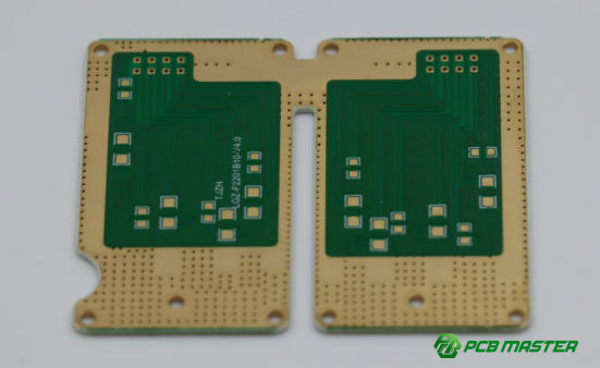
High-density interconnect (HDI) and precision PCB manufacturing demand flawless resin via filling to ensure surface flatness and reliable soldering. Yet, issues like bubbles, sinking, resin overflow, or delamination often challenge production quality. At PCBMASTER, we understand how these obstacles impact your manufacturing outcomes. This article provides a clear overview of common resin via filling problems, their root causes, and practical improvement measures, helping you optimize processes and achieve higher PCB yield and reliability.
Why Do Bubbles or Voids Appear During Resin Via Filling?
Bubbles or voids in resin-filled vias occur when air is trapped inside the hole, resin cannot flow properly, or the filling process parameters are not optimized. These defects affect PCB reliability and soldering quality.
Causes of Bubbles or Voids
1. Insufficient Vacuum Leading to Trapped Air
If the vacuum system is not strong enough during the via filling process, air inside the holes cannot escape. This trapped air forms bubbles that appear in the resin after curing or during grinding. For example, in HDI boards with deep microvias, even a small amount of residual air can cause visible voids on the surface.
2. Poor Resin Flowability
High-viscosity resins may struggle to flow into deep or narrow holes. When resin cannot reach the bottom of the via, voids remain. A common scenario is using room-temperature resin on a PCB with high-density small vias, where the resin may stall mid-hole, leaving tiny air pockets.
3. Incorrect Filling Pressure or Speed
Using too low pressure may fail to fill the via completely, while too high pressure can trap air within the resin. Similarly, moving the filling blade too fast or too slow can disrupt proper resin placement. This is particularly critical for boards with varying via diameters, where uniform pressure is essential.
4. Rough or Moisture-Containing Hole Walls
Contaminated or rough via walls prevent resin from wetting the surface fully. Moisture in the holes can create steam during curing, forming additional bubbles. For example, newly drilled vias without proper cleaning often show micro-voids at the interface between resin and copper plating.
How to Prevent or Fix Bubbles and Voids
1. Optimize Vacuum Parameters
Ensure the via filling machine operates under sufficient vacuum to remove trapped air. For instance, multi-stage vacuum cycles can gradually draw out air in deep microvias, significantly reducing void formation.
2. Adjust Resin Viscosity and Temperature
Use low-viscosity resins or slightly heat the resin before filling to improve flow into deep vias. Heated resin flows more easily, filling narrow holes completely and reducing the chance of air pockets.
3. Fine-Tune Filling Pressure, Speed, and Passes
Adjust the blade pressure, movement speed, and number of filling passes to match via depth and diameter. For example, performing two slower passes rather than one fast pass often eliminates residual bubbles in critical vias.
4. Ensure Clean, Dry, and Properly Treated Hole Walls
Thoroughly clean via walls and remove moisture before filling. Plasma treatment can improve resin wetting on copper or rough surfaces, ensuring resin fully adheres and reducing trapped air. A practical tip is to dry boards in an oven before resin application to minimize void formation.
Why Do Resin-Filled Vias Sink or Appear Uneven After Grinding?
Resin-filled vias can appear sunken or uneven after grinding due to resin shrinkage during curing, excessive material removal during grinding, or insufficient initial resin filling. These issues can affect PCB surface flatness and component assembly.
Causes of Sinking or Uneven Resin Surfaces
1. High Resin Shrinkage After Curing
Resin naturally shrinks as it cures and hardens. If the material has a high cure shrinkage rate, the filled vias can retract below the PCB surface, creating a concave or uneven appearance. For example, standard epoxy resins may shrink up to 3–5%, which is significant for high-density boards with microvias.
2. Excessive Material Removal During Grinding
Grinding is used to level the resin with the PCB surface. However, over-grinding can remove too much resin, leaving the via recessed. This often happens when using coarse grinding wheels or applying too much pressure, especially on boards with small, shallow vias.
3. Insufficient Initial Resin Filling
If the resin filling volume is too low from the start, there is little material to accommodate curing shrinkage or grinding. Even minor resin shrinkage can create noticeable pits, affecting surface uniformity and subsequent component placement.
How to Prevent or Fix Sinking and Uneven Surfaces
1. Use Low-Shrinkage Resins
Selecting resins with a lower cure shrinkage rate reduces the risk of vias sinking. For instance, high-performance epoxy or modified resin formulations can limit shrinkage to less than 1%, ensuring the PCB surface remains flat after curing.
2. Optimize Grinding Process
Adopt a staged grinding approach: first coarse grinding to remove excess resin, followed by fine grinding to achieve surface leveling. Using precision grinding equipment with controlled pressure minimizes the risk of over-removal and uneven surfaces.
3. Increase Resin Filling Volume
Fill vias slightly above the PCB surface to create a grinding margin. This ensures that even after shrinkage and leveling, the vias remain flush with the board. A practical example is adjusting the via filling machine to allow slight overflow, which can later be removed with controlled grinding.
What Are the Main Causes of Resin Discoloration in Filled Vias?
Resin discoloration occurs when the filled vias change color compared to surrounding areas. This problem usually results from chemical incompatibility with surface inks, improper curing conditions, or contamination during production. Discoloration affects PCB appearance and can indicate reliability risks, especially for white or light-colored solder masks.
Causes of Resin Discoloration
1. Chemical Incompatibility Between Resin and Ink
When the resin reacts chemically with the surface ink or solder mask, it can change color after curing. For example, certain epoxies may turn yellow or brown when used over incompatible white solder masks. This reaction is usually invisible before curing but becomes obvious afterward, creating an uneven surface appearance.
2. Improper Curing Conditions
Excessive temperature or prolonged curing time can degrade resin or ink, causing color changes. Overheating may lead to partial charring or darkening of resin, while insufficient temperature may leave resin undercured but with slight discoloration. For instance, curing at temperatures above the resin supplier’s recommended range can cause visible yellowing.
3. Contamination During Production
Dust, oils, or leftover residues from handling can mix with resin during via filling, creating spots or color variations. Even small contaminants on the PCB surface or in the resin supply can lead to localized discoloration, affecting visual quality and sometimes solderability.
How to Prevent or Correct Resin Discoloration
1. Conduct Compatibility Testing Before Mass Production
Always test the selected resin against the board’s ink or solder mask in small batches. Observing reactions in advance prevents large-scale discoloration. For example, PCBMASTER performs pre-production tests on new resin batches with white and black inks to ensure consistent color.
2. Strictly Control Curing Temperature and Time
Follow the resin and ink suppliers’ recommended curing profiles. Use calibrated ovens or hot plates to maintain uniform temperature and prevent overheating. Step-by-step monitoring during curing ensures that resin hardens without darkening or discoloring.
3. Enhance Cleanliness in the Production Environment
Keep the PCB, equipment, and materials free from dust, oil, or other contaminants. Regular cleaning of resin tanks, filling machines, and work surfaces reduces the risk of contamination-related discoloration. For instance, wiping boards with isopropyl alcohol before via filling can prevent minor surface stains.
Why Does Resin Overflow or Contaminate Pads During Via Filling?
Resin overflow or contamination occurs when excess resin escapes from the via and spreads onto nearby solder pads. This problem can cause soldering defects, affect PCB reliability, and reduce visual quality. Overflow is usually caused by overfilling, improper stencil (squeegee) design, or insufficient cleaning after filling.
Causes of Resin Overflow or Pad Contamination
1. Excess Resin Volume or Too High Pressure
Applying too much resin or using excessive filling pressure can force resin out of the via and onto surrounding areas. For example, on densely populated PCBs with fine-pitch pads, even a small overfill can create bridging between pads, leading to short circuits during soldering.
2. Improper Stencil (Mesh/Screen) Design
The size, shape, and thickness of the stencil openings must match the via dimensions and density. Stencils that are too large, misaligned, or too thick can deposit excess resin, causing overflow onto pads. For instance, a misaligned stencil on a 0.2 mm microvia array can result in resin spreading across multiple pads.
3. Untimely Board Cleaning
After via filling, residual resin on the PCB surface must be cleaned before it cures. Failure to clean promptly allows resin to harden on pad surfaces, leading to solderability issues. Even minor residues can interfere with automated pick-and-place and soldering operations.
How to Prevent or Fix Resin Overflow and Pad Contamination
1. Precisely Control Resin Volume and Filling Pressure
Adjust the via filling machine to deliver only the required resin volume at optimal pressure. Conduct small-scale tests to determine the correct parameters for different via sizes. For example, reducing pressure by 10–15% for fine-pitch boards can prevent overflow without affecting via fill quality.
2. Optimize Stencil Opening Size and Thickness
Design stencil openings according to via diameter, depth, and board density. Use thinner stencils for high-density boards to limit excess resin deposition. Regularly inspect stencil alignment to ensure precise resin placement.
3. Clean the PCB Immediately After Filling
Remove any resin residues from the board surface before it cures. Use isopropyl alcohol or dedicated cleaning equipment to wipe pads and board surfaces. Immediate cleaning ensures that solder pads remain fully exposed for high-quality soldering.
How Can Incomplete Via Filling Be Improved?
Incomplete filling occurs when resin does not fully occupy the via, leaving gaps or voids. This can reduce PCB reliability, create soldering defects, and impact mechanical strength. Causes include high resin viscosity, insufficient filling passes, blockages inside the via, and inadequate vacuum or pressure during the process.
Causes of Incomplete Filling
1. High Resin Viscosity
Resins that are too thick cannot flow easily into deep or narrow vias. High-viscosity resin may leave voids near the bottom, particularly in high-density PCBs with microvias. For example, using room-temperature epoxy on 0.2 mm diameter microvias can result in incomplete filling if viscosity is not optimized.
2. Insufficient Filling Passes
Performing only a single filling pass may not allow resin to fully occupy all vias, especially deep or high aspect ratio ones. Some boards require two or more passes to ensure complete resin coverage.
3. Blockages Inside the Via
Debris, leftover dry film, or copper residue can block vias and prevent resin from flowing through. Even small particles can create gaps that affect both electrical connectivity and surface leveling.
4. Inadequate Vacuum or Pressure
Vacuum and pressure are essential for driving resin into the via. Low vacuum leaves trapped air, while insufficient pressure fails to push resin to the via bottom, causing incomplete fills.
How to Improve Incomplete Via Filling
1. Improve Resin Flowability
Use lower-viscosity resin or preheat resin slightly to enhance flow. Proper resin flow ensures it reaches the bottom of the via, even in deep microvias.
2. Add a Second Filling Pass
Implement a two-pass via filling process for deep or high-density boards. The first pass fills most of the via, and the second pass ensures complete filling and compensates for any shrinkage.
3. Strengthen Via Cleaning
Clean vias thoroughly to remove debris, dry film fragments, and copper residues. Techniques like plasma cleaning or ultrasonic cleaning can ensure vias are unobstructed and ready for resin filling.
4. Ensure Equipment Pressure and Vacuum Are Optimal
Regularly calibrate and maintain vacuum and pressure systems on filling machines. Proper vacuum removes trapped air, and correct pressure pushes resin fully into the via, reducing incomplete fills.
How Can Delamination or Board Cracking Be Prevented After Resin Via Filling?
Delamination or cracking occurs when resin-filled vias separate from the via walls or cause the PCB layers to separate under heat or mechanical stress. This reduces reliability and can lead to electrical failures. Causes include poor resin adhesion, thermal mismatch, and incomplete curing.
Causes of Delamination or Cracking
1. Poor Adhesion Between Resin and Via Walls
If resin does not bond strongly to the copper or substrate inside the via, mechanical or thermal stress can cause separation. For example, via walls with insufficient copper plating or contamination may prevent resin from adhering properly, creating weak spots prone to delamination.
2. Thermal Mismatch of Resin (Low Tg or CTE Differences)
Resins with low glass transition temperature (Tg) or a coefficient of thermal expansion (CTE) that differs significantly from the PCB substrate can expand or contract unevenly during heating. This stress may crack the resin or separate PCB layers, especially during soldering or thermal cycling.
3. Incomplete Resin Curing
Uncured or partially cured resin cannot maintain mechanical strength, causing internal voids and pressure buildup during thermal processes. Incomplete curing can result from incorrect temperature profiles, too short curing times, or uneven heat distribution in the oven.
How to Prevent Delamination or Cracking
1. Strengthen Resin-to-Via Wall Adhesion
Ensure high-quality copper plating and, if needed, perform plasma treatment to improve resin wetting. Well-plated vias provide a strong surface for resin bonding. For instance, boards that undergo electroplating and plasma cleaning before filling show significantly lower delamination rates.
2. Use High Tg, Low CTE Resin Matched to the Substrate
Select resins with higher glass transition temperatures and thermal expansion similar to the PCB material. This minimizes thermal stress during heating cycles and ensures the resin and substrate expand or contract together, reducing cracking risk.
3. Optimize Curing Profile and Verify Cure Degree
Follow precise curing temperature and time recommended by the resin supplier. Use Differential Scanning Calorimetry (DSC) testing to confirm the resin is fully cured. Proper curing ensures mechanical integrity and prevents internal stress that can lead to delamination.
How Can Resin Via Filling Quality Be Stabilized Through Systematic Control?
Brief Answer: Consistent resin via filling quality requires a system-level approach that combines material inspection, equipment maintenance, process standardization, production monitoring, and staff training. These measures prevent defects such as voids, sinking, discoloration, and delamination, ensuring high-yield and reliable PCBs.
Incoming Material Inspection and Control
Check Key Resin Properties (Viscosity, Shrinkage, Tg)
Before production, inspect resin batches for critical properties including viscosity, curing shrinkage, and glass transition temperature (Tg). Variations in these parameters can directly impact via filling, surface flatness, and thermal reliability. For example, a resin batch with higher-than-expected viscosity may fail to fully fill microvias, leading to voids and soldering issues.
Real-life Practice: PCBMASTER routinely tests every resin batch for viscosity and Tg to ensure compatibility with high-density PCBs. Only compliant batches enter production.
Equipment Maintenance and Process Standardization
Regular Calibration of Machines
Ensure via filling machines, vacuum systems, and grinders are calibrated and maintained regularly. Equipment inconsistencies can lead to incomplete fills or uneven surfaces.
Define Optimal Process Windows Using DOE
Use Design of Experiments (DOE) to identify the best combination of pressure, speed, vacuum, temperature, and curing profiles. Standardizing these parameters ensures stable filling results across different boards and batches.
Example: DOE testing at PCBMASTER revealed optimal blade speed and vacuum levels for 0.2 mm microvias, reducing void defects by 40%.
First Article Inspection and Production Monitoring
Use Cross-Sectional Analysis to Confirm Filling
Perform slice or cross-sectional analysis on the first boards to ensure vias are fully filled and cured. This identifies potential problems before full-scale production.
Implement Regular Sampling During Production
Periodically inspect random boards during manufacturing to verify consistent filling quality. Early detection of anomalies prevents large-scale defects.
Case Example: Random sampling on HDI boards enabled PCBMASTER to detect a subtle pressure drop in the filling machine before it caused widespread voids.
Staff Training and Standard Operating Procedures
Train Operators on Key Control Points
Ensure staff understand critical factors like resin properties, filling pressure, vacuum settings, and cleaning protocols. Skilled operators can maintain process quality consistently.
Enable Immediate Issue Detection and Response
Operators trained to recognize abnormal filling or resin behavior can intervene quickly, preventing defective boards from progressing down the line.
Practical Approach: PCBMASTER provides hands-on training for new operators, including troubleshooting voids, resin overflow, and surface sinking, ensuring high-quality outcomes.
Conclusion
Consistently achieving high-quality resin-filled vias requires more than just addressing individual defects—it demands a holistic approach that combines careful material selection, precise process control, thorough inspection, and skilled operators. By understanding the root causes of common issues like voids, sinking, discoloration, overflow, and delamination, and applying targeted solutions, manufacturers can significantly improve PCB reliability and appearance.
At PCBMASTER, we integrate these best practices into every stage of production, from incoming material checks to final inspection, ensuring that each board meets the highest standards. With our expertise in advanced PCB and HDI manufacturing, we help customers achieve exceptional via filling quality and long-term reliability across all their projects.
FAQs
Will increasing the number of via filling passes affect production efficiency?
Yes, adding extra filling passes can slightly reduce production speed because each pass takes additional time. However, it often ensures complete via filling and reduces defects, which can save time and costs associated with rework or failed boards. Balancing efficiency and quality is key.
How to choose a low-shrinkage resin to prevent post-grinding depressions?
Select resins with a low curing shrinkage rate, often specified in the technical datasheet by the manufacturer. Epoxy formulations designed for via filling usually indicate shrinkage percentages. Pre-testing the resin on sample boards is recommended to ensure it maintains surface flatness after grinding.
Can resin overflow on solder pads be repaired?
Yes, resin overflow can be removed if it is still uncured. Use solvents like isopropyl alcohol or specialized cleaning equipment to wipe pads carefully. Once cured, resin is difficult to remove without damaging the PCB, so timely cleaning is critical.
Are bubble issues more likely to occur in high-density interconnect (HDI) boards?
Yes, HDI boards have smaller vias and higher aspect ratios, which make it harder for resin to flow and for trapped air to escape. This increases the risk of bubbles or voids, requiring optimized vacuum, resin viscosity, and filling parameters.
Does delamination or board cracking relate to PCB thickness?
Yes, thicker or multi-layer boards can experience higher internal stresses during thermal cycles. Thicker boards may require resins with matched thermal expansion (CTE) and high glass transition temperatures (Tg) to reduce the risk of delamination or cracking.

