


Resin Plugged Vias and Copper Plating Planarization: A Complete PCB Manufacturing Guide
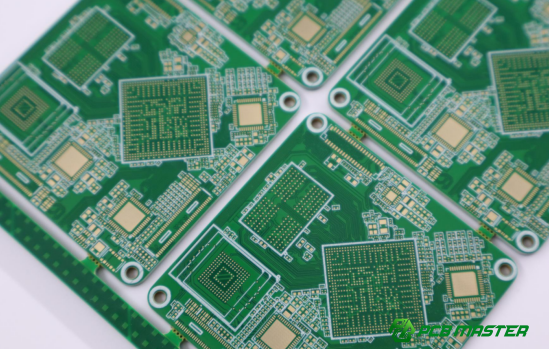
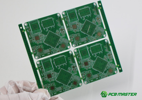
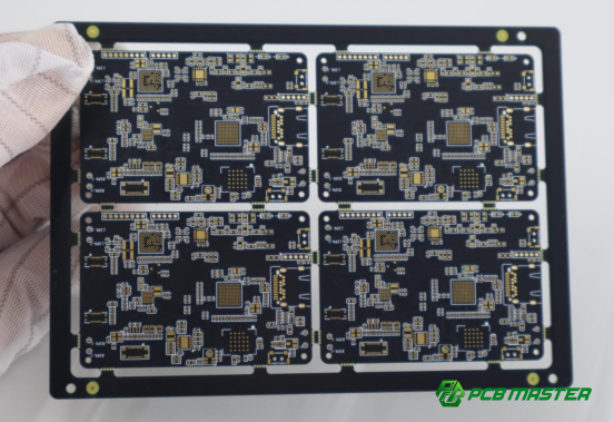
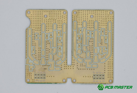
Resin-filled vias with copper plating, often called “via-in-pad” plating, is a high-precision PCB process designed to create completely flat board surfaces by filling vias with resin and leveling them before plating. This technique is essential for high-density, fine-pitch designs, as it prevents solder defects, improves reliability, and maximizes routing efficiency.
As a seasoned PCB and PCBA supplier, PCBMASTER has perfected this process to meet the most stringent industry standards. In the following sections, we will walk you through the complete resin-filled, copper-plated PCB process, detailing each stage, key control points, and the practical advantages it brings to advanced PCB manufacturing.
Stage 1: Drilling and Preparation Before Resin-Filled and Copper-Plated PCB
Drilling and preparation involve precisely creating through-holes and buried vias after PCB lamination and applying a thin copper layer to the holes to ensure proper metallization and resin adhesion.
What are the drilling steps after PCB lamination?
After PCB lamination, the board is drilled to create the holes needed for electrical connections.
Once the PCB layers are laminated, precise holes must be drilled to form through-holes and buried vias. Through-holes connect the top and bottom layers of the PCB, while buried vias only connect internal layers without reaching the surface. The drilling process uses CNC machines with micro-precision tools to ensure each hole meets the design specifications.
Precision and hole diameter control are crucial. Even a tiny deviation can affect electrical conductivity, resin filling, and the final surface flatness. For example, in a 6-layer HDI board, a through-hole diameter may need to stay within ±5 microns to avoid misalignment. Proper drilling ensures the vias are ready for metal coating and prevents later defects during resin filling and copper plating.
What preparation is needed before via metallization?
Before metallization, the holes need a thin conductive layer to allow copper plating.
The first step is chemical copper deposition, which coats the drilled holes with a thin, uniform layer of copper. This layer is not thick but makes the hole walls electrically conductive, allowing the next step—full board electroplating—to work. Chemical copper ensures consistent metal adhesion in every via, even tiny buried ones.
Next, full-board copper electroplating thickens the copper layer inside and around the vias, typically to 5–8 microns. This provides mechanical strength and a reliable conductive path, supporting resin filling later. In practice, without proper electroplating, the resin may not bond well, and the final flat surface after plating could be uneven.
Example: In HDI PCBs for smartphones, electroplating before resin filling prevents weak connections in blind vias under BGA pads, ensuring both reliability and soldering quality.
Stage 2: Resin-Filled Vias
Resin-filled vias are PCB holes that are completely filled with resin to create a flat, reliable surface for high-density, fine-pitch components.
Why is hole cleaning and preheating important?
Cleaning and preheating the PCB ensures resin fills the vias completely and bonds properly.
Before resin filling, hole cleaning removes dust, dirt, and oil from the drilled holes and board surface. Any contamination can trap air bubbles or prevent the resin from adhering to the copper, which may lead to voids, weak connections, or solder defects. For example, in a BGA pad via, even a tiny particle can cause a solder joint to fail during reflow.
Preheating the PCB lowers the resin’s viscosity, allowing it to flow more easily into each via. A warmer board makes resin penetration faster and more uniform. In practice, preheating is especially critical for fine-pitch HDI boards where vias are less than 100 microns in diameter. Combining cleaning and preheating maximizes fill quality and ensures long-term reliability.
How does vacuum resin filling work, and what resin should be used?
Vacuum resin filling uses negative pressure to push resin into vias, and the right resin ensures strong adhesion and proper curing.
Vacuum resin filling works by placing the PCB in a vacuum chamber and applying negative pressure. Air inside the vias is removed, and then resin is injected, forcing it to completely fill each via without leaving bubbles. This method is highly effective for blind and buried vias in HDI PCBs.
Resin selection is critical. Epoxy-based resins are commonly used because they have excellent adhesion to copper, low thermal expansion, and appropriate hardness for later surface grinding. Resins must also be compatible with the curing process to turn from liquid to solid without shrinkage that could create gaps. Using the correct resin type ensures both via reliability and flat surface formation after plating.
How is excess resin removed and the board surface leveled?
Scraping removes extra resin and ensures a flat, uniform PCB surface.
After filling, scraping or squeegeeing removes resin that overflows the via openings. Operators use a precision blade to gently level the surface, leaving the resin flush or slightly below the copper plane. Proper scraping prevents bumps that could interfere with BGA soldering or cause uneven plating.
Control points: Complete filling without overfilling maintains via integrity, while careful scraping maintains surface flatness. For example, in high-density smartphone PCBs, scraping resin too aggressively could expose copper or damage the surrounding solder mask. Following correct techniques ensures a smooth, planar surface ready for resin curing and subsequent copper plating.
Stage 3: Resin Curing and Surface Grinding
Resin curing solidifies the filled vias to ensure mechanical strength and electrical reliability, while surface grinding levels the board so the resin sits slightly below the copper, creating a perfectly flat surface for subsequent plating.
What is the resin curing process?
Resin curing turns the filled resin from liquid to solid, giving it mechanical strength and electrical stability.
After resin filling, the PCB is placed in an oven for curing. The process uses a carefully controlled temperature curve, gradually heating the board to the resin’s specified curing temperature and holding it for a set time. This ensures complete chemical reaction without causing shrinkage or stress cracks.
Proper curing affects both mechanical strength and electrical performance. Fully cured resin prevents via collapse, maintains planarity, and insulates the via from surrounding copper layers. For example, in HDI boards for industrial controllers, insufficient curing can lead to cracked vias and short circuits during soldering. Following the correct temperature curve and curing time is critical for reliability and subsequent grinding.
How is surface grinding performed to ensure flatness?
Answer: Grinding removes excess resin and levels the PCB surface, preparing it for plating.
Surface grinding uses two main steps: coarse grinding followed by fine grinding. Coarse grinding removes most of the resin protruding above the copper surface. Fine grinding smooths the resin and ensures a flat surface with high precision.
Flatness standard: The resin surface should remain slightly below the copper plane by 1–3 μm. This small gap allows later copper plating to fill the resin slightly and achieve a perfectly planar board.
Common grinding issues and solutions:
l Over-grinding: Can damage copper pads or expose vias. Solution: use fine-grit sanding belts and precise pressure control.
l Under-grinding: Leaves resin bumps, affecting component placement. Solution: repeat fine grinding and inspect with optical measurement tools.
Proper surface grinding ensures uniformity, supports fine-pitch BGA assembly, and is critical for resin-filled, copper-plated PCB reliability.
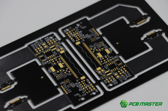
Stage 4: Copper Plating and Surface Planarization
Copper plating and surface planarization create a perfectly flat PCB surface by depositing uniform copper over resin-filled vias, ensuring strong adhesion and reliable soldering for fine-pitch components.
Why is board cleaning and micro-etching important?
Cleaning and micro-etching prepare the PCB surface for strong copper adhesion and remove any contaminants.
After resin grinding, the board surface often contains resin dust and particles. These small residues can prevent copper from bonding properly, leading to weak plating and potential delamination. Cleaning uses chemical solutions and ultrasonic washing to remove dust and oils.
Micro-etching uses a mild acid solution to slightly roughen the copper surface. This process increases the bonding strength between the existing copper and the new electroplated copper layer. For example, in HDI PCBs, micro-etching ensures the flat copper layer adheres strongly over resin-filled vias, preventing peeling during reflow soldering. Proper cleaning and micro-etching are critical to maintain long-term PCB reliability and surface uniformity.
How does secondary full-board copper plating (planarization) work?
Secondary copper plating deposits a uniform copper layer, filling any depressions on the resin surface to create a completely flat PCB.
During secondary full-board electroplating, copper is deposited evenly across the entire PCB surface, including areas over resin-filled vias. Since the vias are already filled with resin, copper only accumulates on the board surface, leveling the slight depressions and producing a perfectly flat surface.
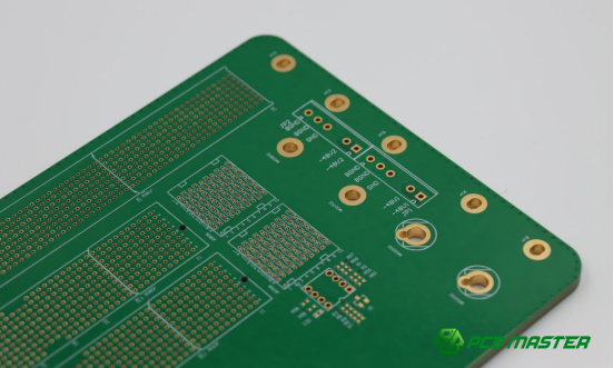
Surface flatness impact: A planar surface is essential for fine-pitch BGA assembly and outer-layer circuit patterning. If the board surface is uneven, solder paste may not spread evenly, causing soldering defects or connectivity issues. For instance, in high-density smartphone PCBs, flat surfaces after copper plating ensure reliable solder joints for 0.3 mm pitch BGA components.
This step is the final preparation before outer-layer circuit fabrication, and controlling copper deposition uniformity directly affects PCB quality, reliability, and manufacturability.
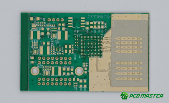
Stage 5: Outer Layer Pattern Transfer and PCB Finishing
Outer layer pattern transfer and PCB finishing involve creating precise circuit patterns on a flat PCB surface through photolithography, thickening and protecting the copper with electroplating and protective layers, and applying solder masks and surface finishes to ensure long-term reliability and soldering quality.
How is outer layer pattern transferred onto the PCB?
The outer layer circuit is created using a photolithography process that requires a flat, clean board surface.
The process starts with photoresist coating on the fully planarized PCB. This can be done using dry-film or liquid photoresist. After coating, the PCB is exposed to UV light through a photomask that defines the circuit pattern. The exposed areas are then developed, washing away the unexposed photoresist to reveal the copper underneath.
A flat surface is crucial for this step. If the PCB surface has bumps or depressions, the photoresist may not adhere evenly, causing blurred or incomplete circuit patterns. For example, HDI boards with 0.3 mm pitch BGA pads require extremely flat surfaces to prevent misalignment and short circuits during assembly. Proper outer layer pattern transfer ensures accurate and reliable circuit formation.
How are patterns electroplated and protected during etching?
Electroplating and protective layers strengthen circuits and protect copper during etching.
After pattern transfer, the exposed copper is thickened through additive electroplating, enhancing electrical conductivity and mechanical strength. A tin (or other protective layer) is applied over the electroplated areas to shield them during the etching process.
Next, the board undergoes etching, which removes unwanted copper outside the circuit patterns. Following etching, solder mask application and surface finishes such as ENIG (Electroless Nickel Immersion Gold) or OSP (Organic Solderability Preservative) are applied to protect the copper, prevent oxidation, and facilitate reliable soldering. For example, in smartphone PCBs, these steps prevent shorts, improve solder adhesion, and ensure long-term durability under repeated thermal cycles.
How is finished PCB quality ensured?
Finished PCBs are tested to ensure reliable soldering and long-term performance.
Soldering reliability tests simulate reflow conditions to verify that the PCB pads and vias maintain integrity during actual assembly. CAF (Conductive Anodic Filament) resistance testing ensures the board can withstand high humidity and voltage stress without forming unwanted conductive paths.
High-quality resin-filled, copper-plated PCBs demonstrate enhanced reliability, with lower risk of via failure, short circuits, or delamination. For instance, industrial PCBs with resin-filled vias show superior CAF resistance compared to standard boards, making them suitable for high-performance and high-density applications. These tests confirm that the PCB is ready for assembly and long-term operation.
Key Process Control Points for Resin-Filled and Copper-Plated PCBs
The key process control points for resin-filled and copper-plated PCBs are selecting the right resin, ensuring bubble-free via filling, monitoring grinding flatness, and performing thorough pre-plating cleaning and micro-etching to guarantee reliability and surface planarity.
What are the resin selection criteria?
Choosing the right resin ensures mechanical stability, thermal compatibility, and ease of grinding.
Thermal expansion coefficient (CTE): The resin must have a CTE similar to copper and the PCB substrate to prevent stress cracks during heating cycles. A mismatch in thermal expansion can lead to delamination or via cracking during reflow soldering.
Copper adhesion and grinding hardness: The resin must bond strongly to copper and be hard enough to withstand surface grinding without chipping or creating uneven areas. For example, in HDI boards for smartphones, using a low-quality resin can lead to via popping or uneven plating, causing solder defects. Choosing resins with optimized CTE, adhesion, and hardness ensures both flatness and long-term reliability.
How is bubble-free via filling ensured?
Proper vacuum settings and resin flow control prevent air pockets inside vias.
Vacuum machine parameter optimization: The vacuum pressure, resin injection speed, and preheating temperature must be carefully controlled. These settings ensure the resin fully penetrates the via, displacing all air and avoiding voids.
Reflow soldering safety: Air bubbles inside vias expand under heat, potentially causing solder bumps or board warping during reflow. Maintaining bubble-free filling guarantees both mechanical integrity and reliable soldering. For example, in BGA applications, a single trapped bubble can lead to an open circuit, so controlling the vacuum parameters is critical.
Why monitor grinding flatness?
Surface grinding ensures the resin is level with surrounding copper without damaging the PCB.
l Avoiding uneven surfaces: Under-grinding leaves bumps that interfere with component placement.
l Avoiding copper damage: Over-grinding can expose copper or scratch the surrounding pads, reducing reliability.
Monitoring grinding flatness typically uses optical inspection or laser measurement systems. For instance, in HDI boards with 0.3 mm pitch BGAs, precise flatness ensures uniform solder paste application, preventing solder bridging and open joints. Accurate grinding control is essential for subsequent copper plating and component assembly.
Why is cleaning and micro-etching necessary before copper plating?
Cleaning and micro-etching prevent copper delamination and ensure strong plating adhesion.
l Surface cleaning: Residual dust, resin particles, or oils can weaken copper bonding, causing plating defects or delamination.
l Micro-etching: A light acid treatment roughens the copper surface, increasing adhesion for the next plating step.
For example, in high-density industrial PCBs, inadequate cleaning or micro-etching may result in partial plating or copper lifting, compromising reliability. Performing thorough cleaning and micro-etching is a critical control point to maintain the integrity of resin-filled, copper-plated vias.
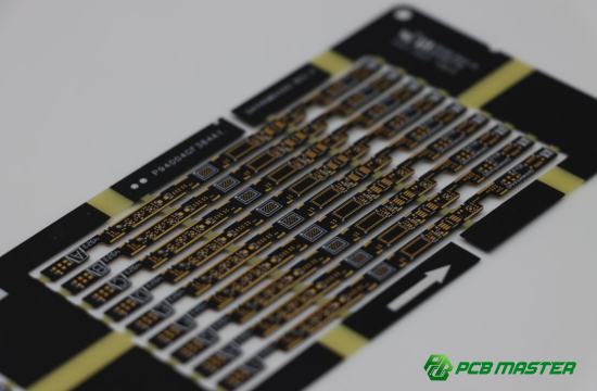
Core Advantages of Resin-Filled and Copper-Plated PCBs
Resin-filled and copper-plated PCBs provide higher routing density, improved soldering reliability, and enhanced long-term durability by supporting via-in-pad designs, preventing solder defects, and increasing CAF resistance.
How does this process support via-in-pad designs?
Resin-filled vias allow vias to be placed directly under component pads, saving space and increasing routing density.
With via-in-pad design, vias are filled and leveled with resin so they don’t interfere with component soldering. This design saves routing space, making it possible to fit more connections in a smaller area. It also improves circuit density, which is critical for compact devices like smartphones or miniaturized IoT modules.
Example: In a 6-layer HDI smartphone PCB, via-in-pad allows multiple signal and power layers to converge under a BGA pad without creating solder wicking problems, maximizing both layout flexibility and board performance.
How does it improve soldering quality?
Resin-filled vias prevent solder from flowing into vias, ensuring reliable solder joints.
Preventing solder shorts: Open vias under pads can cause solder to flow through during reflow, leading to short circuits or insufficient solder joints. Resin filling blocks these pathways.
BGA solder reliability: For fine-pitch BGAs, a flat, resin-filled via prevents solder ball collapse or bridging, improving joint reliability and electrical performance. For instance, in high-density computing boards, resin-filled via-in-pad ensures consistent solder joint height across the BGA, reducing the risk of thermal cycling failures.
How does it enhance long-term PCB reliability?
Resin filling protects vias from chemical damage and increases CAF resistance, extending PCB lifespan.
Preventing chemical residue: Resin-filled vias block etchants or flux residues from accumulating inside vias, which could otherwise lead to corrosion or weak connections.
Improved CAF resistance and lifespan: CAF (Conductive Anodic Filament) forms under high humidity and voltage stress, causing shorts. Resin-filled vias reduce CAF formation, making PCBs more durable in harsh environments. For example, industrial control boards using resin-filled vias demonstrate longer operational life and higher reliability compared to standard vias.
Conclusion
As electronic devices become increasingly compact and complex, the demand for reliable, high-density PCBs continues to grow. Mastering advanced processes like resin-filled via and copper planarization is no longer optional—it’s essential for ensuring superior soldering quality, enhanced signal integrity, and long-term board reliability.
For companies seeking consistent, high-performance PCB solutions, PCBMASTER brings decades of expertise and precision in implementing these advanced manufacturing processes. By combining state-of-the-art equipment, rigorous quality control, and in-depth process knowledge, PCBMASTER ensures every board meets the strictest industry standards, delivering reliability and performance that engineers can trust.
FAQs
1. What types of PCBs are suitable for resin-filled and copper-planarized vias?
Resin-filled and copper-planarized vias are ideal for high-density interconnect (HDI) PCBs, multi-layer boards, and designs with via-in-pad layouts. These PCBs require flat surfaces for fine-pitch components like BGAs, and the process helps maximize routing space while maintaining reliability in compact electronic devices.
2. What problems can occur if bubbles form in the filled resin?
Air bubbles inside resin-filled vias can expand during reflow soldering, causing solder bumps, via collapse, or board warping. This can lead to open circuits, short circuits, or unreliable solder joints, especially in high-density boards with fine-pitch components. Proper vacuum filling is essential to avoid these issues.
3. How does insufficient surface flatness affect BGA soldering?
If the resin surface is not leveled properly, solder paste may not spread evenly on BGA pads, leading to solder bridging, insufficient solder joints, or open circuits. Maintaining a flat surface, slightly below the copper plane (1–3 μm), ensures reliable soldering for high-density components.
4. Why might the surface remain uneven after copper planarization?
Uneven surfaces after plating can result from incomplete resin filling, residual dust, improper micro-etching, or non-uniform copper deposition. These issues can affect outer-layer pattern transfer and soldering quality, so careful process control at each stage is critical.
5. How do you select the right epoxy resin for via filling?
Choose a resin with low thermal expansion (CTE) compatible with copper and substrate, strong adhesion to copper, and appropriate hardness for surface grinding. The resin should also have good electrical insulation and proper curing properties to ensure flatness, reliability, and long-term durability of the PCB.

