


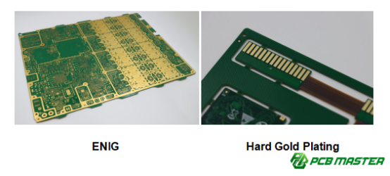
Are ENIG and Hard Gold Nickel Layers the Same? Key Differences Explained
Are ENIG and hard gold nickel layers the same? No. This is one of the most common misunderstandings in PCB surface finishing. Although both processes use a nickel layer between copper and gold, the nickel itself is fundamentally different.
In ENIG (Electroless Nickel Immersion Gold) , the nickel layer is a nickel-phosphorus (Ni-P) alloy created through a chemical deposition process. Its primary role is to provide a reliable solderable surface and act as a diffusion barrier for SMT pads, BGA packages, and other fine-pitch assemblies.
By contrast, the nickel layer used in hard gold plating is typically electroplated pure nickel . It is designed to support thick gold deposits, improve wear resistance, and maintain stable electrical contact in applications such as gold fingers and connectors that experience repeated insertion and removal.
The confusion arises because both finishes have a similar layer sequence—copper, nickel, then gold—and the nickel layer is hidden beneath the gold coating. From the outside, they often look identical. However, once the nickel composition, deposition method, and intended function are examined, the differences become clear. Understanding these distinctions is the key to choosing the right PCB surface finish for the intended application.
What Is the Difference in Composition Between ENIG Nickel Layer and Hard Gold Nickel Layer?
The ENIG nickel layer is a nickel–phosphorus alloy (Ni-P), while the hard gold plating nickel layer is primarily pure electroplated nickel.
What is the real composition of ENIG nickel layer?
The ENIG nickel layer is a nickel–phosphorus alloy (Ni-P), not pure nickel.
The ENIG (Electroless Nickel Immersion Gold) process forms a chemical nickel layer made of nickel-phosphorus alloy (Ni-P) . This means phosphorus atoms are intentionally co-deposited with nickel during electroless plating. This is a key distinction in ENIG nickel composition vs . hard gold nickel composition .
A key control factor is phosphorus content , which directly affects performance. In most PCB surface finish applications, the phosphorus level is carefully controlled because it determines hardness, corrosion resistance, and magnetic behavior. If phosphorus is too low or too high, the coating performance becomes unstable.
The most common system used in PCB manufacturing is medium-phosphorus Ni-P (6%–9% phosphorus) . This range provides a balanced combination of:
- Good solderability (important for SMT pads and BGA)
- Stable corrosion resistance
- Controlled internal stress
Real-world example: In an ENIG PCB pad used for BGA packaging, the Ni-P layer acts like a “protective barrier wall” between copper and gold. It prevents copper diffusion while still allowing reliable soldering during SMT reflow.
What is the real composition of hard gold (electroplated gold) nickel layer?
The nickel layer in hard gold plating is mainly pure nickel, typically electrodeposited as low-stress nickel.
In hard gold plating (electroplated gold system) , the nickel layer underneath is usually electroplated pure nickel , not an alloy. This layer is commonly called a barrier layer and is designed to support wear resistance and electrical contact stability.
There are two common types used in industry:
- Bright nickel: Smooth surface, good conductivity, widely used in general electronics.
- Low-stress matte nickel: Designed to reduce internal stress and improve flexibility, especially in connector applications.
The key requirement is nickel purity and coating quality , because this layer must:
- Prevent copper diffusion into gold
- Maintain low contact resistance
- Provide mechanical strength for repeated plugging/unplugging
Real-world example: In a PCB gold finger (edge connector), the nickel layer acts like a “hard backbone.” When the card is inserted and removed thousands of times, this pure nickel layer prevents wear and keeps electrical contact stable.
What is the fundamental difference between nickel–phosphorus alloy and pure nickel?
The main difference is that ENIG uses an alloy (Ni-P), while hard gold uses pure nickel, leading to completely different structure and properties.
| Comparison Dimension | ENIG Nickel Layer (Ni-P Alloy) | Hard Gold Nickel Layer (Pure Nickel) |
| Material Type | Nickel + phosphorus alloy (Ni-P) | Almost pure nickel, minimal alloying elements |
| Core Composition Meaning | Alloy system with controlled phosphorus content | Single-metal system (Ni dominant) |
| Crystal Structure | Amorphous or micro-crystalline (high P content) | Fully crystalline structure |
| Grain Boundaries | No clear grain boundaries when phosphorus is high | Clear grain boundaries present |
| Structural Analogy | “Glass-like solid armor” (uniform, non-granular) | “Metal mesh armor” (structured and grain-based) |
| Property Origin | Performance mainly controlled by phosphorus content | Performance controlled by crystal structure + plating stress |
| Magnetism Behavior | High-P ENIG is weakly magnetic or non-magnetic | Pure nickel is ferromagnetic |
| Corrosion Behavior | Strong resistance to intergranular corrosion | More sensitive to corrosion if pores exist |
| Reliability Behavior | More stable in chemical and soldering environments | More dependent on plating quality and pore control |
| Primary PCB Application | SMT pads, BGA soldering surfaces | Gold fingers, connectors, mechanical contact areas |
| Design Focus | Solderability + diffusion barrier performance | Wear resistance + electrical contact stability |

What Are the Physical Property Differences Between ENIG Nickel Layer and Hard Gold Nickel Layer?
The ENIG nickel layer (Ni-P alloy) is harder, often amorphous, non-magnetic, and more corrosion-resistant, while the hard gold nickel layer (pure nickel) is crystalline, more ductile, magnetic, and better suited for mechanical contact applications.
What are the crystal structure differences?
ENIG nickel is mostly amorphous or mixed microcrystalline, while hard gold nickel is a fully crystalline metal structure.
The ENIG (Electroless Nickel Immersion Gold) nickel layer is a nickel–phosphorus alloy (Ni-P) . When phosphorus content is medium to high, the structure becomes amorphous or microcrystalline , meaning there are no clear grain boundaries. This is a key point in ENIG nickel vs . hard gold nickel physical properties .
In contrast, the hard gold plating nickel layer is electroplated pure nickel , which naturally forms a fine crystalline structure with clear grain boundaries .
The presence or absence of grain boundaries matters:
- ENIG (no clear grains) → better corrosion resistance, more uniform structure
- Hard gold nickel (grain structure exists) → better mechanical flexibility and conductivity stability under stress
Example: In a PCB pad, ENIG behaves like a smooth “glass-like layer,” while pure nickel behaves like a “metal mesh,” where grains can influence wear and stress behavior.
What are the differences in hardness and mechanical properties?
ENIG Ni-P is harder, while pure nickel is more ductile and flexible.
The nickel-phosphorus alloy in ENIG is significantly harder , typically around 450–600 HV (before heat treatment). After heat treatment, hardness can increase further, which makes it more resistant to deformation. This is important for ENIG hardness vs . hard gold nickel layer comparison .
On the other hand, pure nickel used in hard gold systems has better ductility , meaning it can bend or deform slightly without cracking. This makes it ideal for repeated mechanical contact.
Key behavior differences:
- ENIG: high hardness, lower flexibility → good for solder pads
- Hard gold nickel: moderate hardness, high flexibility → good for connectors
Real example: A BGA pad (ENIG) only needs to survive soldering once, so hardness is not a problem. But a gold finger connector must survive thousands of insertions, so ductility is critical.
How does magnetic behavior differ?
Pure nickel is magnetic, while high-phosphorus ENIG nickel is almost non-magnetic.
Pure nickel in hard gold plating is ferromagnetic , meaning it can be attracted by a magnetic field. This is a normal property of crystalline nickel and is important in some electronic environments.
In contrast, ENIG nickel–phosphorus alloy becomes non-magnetic when phosphorus content is above ~8% . This is because the amorphous structure disrupts magnetic ordering.
Impact in real applications:
- ENIG: suitable for high-frequency and RF-related PCB areas
- Hard gold nickel: magnetic behavior usually not an issue, but can matter in sensitive sensor or RF designs
Example: In RF PCBs, ENIG is often preferred because reduced magnetism helps lower signal disturbance compared to pure nickel structures.
What are the conductivity differences?
Pure nickel conducts electricity more predictably, while ENIG Ni-P has reduced conductivity due to phosphorus content and amorphous structure.
Pure nickel has a stable electrical resistivity of about 6.9 × 10⁻⁶ Ω·cm , making it a consistent conductive barrier layer in hard gold systems.
ENIG nickel–phosphorus alloy has higher resistivity , because phosphorus atoms disrupt electron flow and the amorphous structure reduces conductivity pathways.
In real PCB design:
- ENIG nickel is mainly a diffusion barrier, not a current-carrying layer
- Hard gold nickel is a contact layer, supporting stable electrical connection under mechanical stress
Example: In a gold finger connector, pure nickel ensures stable low-resistance contact. In ENIG pads, conductivity is not critical because current flows through solder joints after assembly.
How does corrosion resistance differ?
ENIG nickel is more corrosion-resistant due to its amorphous structure, while pure nickel is more vulnerable to pore-related corrosion.
The ENIG Ni-P layer has no grain boundaries , especially in medium/high phosphorus systems. This eliminates weak points where corrosion can start, making it highly resistant to intergranular corrosion and salt spray environments .
Pure nickel in hard gold plating has a crystalline structure with grain boundaries. If there are micro-pores or defects , corrosive agents like chlorides can penetrate and attack the underlying copper layer.
Performance comparison:
- ENIG: excellent corrosion resistance, stable in humid/salt environments
- Hard gold nickel: good protection, but depends heavily on plating quality and porosity control
Example: In coastal electronic devices, ENIG finishes often last longer without corrosion issues compared to poorly controlled hard gold nickel layers.
Comparison table of physical properties
| Property | ENIG Nickel (Ni-P Alloy) | Hard Gold Nickel (Pure Nickel) |
| Crystal Structure | Amorphous / microcrystalline | Fine crystalline |
| Grain Boundaries | None or minimal | Present |
| Hardness | High (450–600 HV+) | Moderate (150–250 HV) |
| Ductility | Lower | Higher |
| Magnetism | Non-magnetic (high P) | Ferromagnetic |
| Electrical Conductivity | Lower (higher resistivity) | Stable and predictable |
| Corrosion Resistance | Excellent (no grain corrosion paths) | Good but pore-sensitive |
| Main Application | SMT pads, BGA, soldering surfaces | Gold fingers, connectors, wear surfaces |
Simple takeaway:
- ENIG = hard, corrosion-resistant, solder-friendly
- Hard gold nickel = flexible, conductive, wear-resistant
Why Are the Nickel Deposition Methods Different Between ENIG and Hard Gold Plating?
ENIG uses a chemical electroless self-catalytic process that deposits a Ni-P alloy uniformly without external current, while hard gold plating uses an electroplating process driven by electric current to deposit pure nickel, leading to different control mechanisms and coating behaviors.
Why does ENIG use electroless autocatalytic deposition?
ENIG uses a chemical (electroless) self-catalytic reaction that does not require external current.
In ENIG (Electroless Nickel Immersion Gold) , the nickel layer is formed by a chemical reduction reaction in a liquid bath , not by electricity. This is called autocatalytic electroless nickel deposition . The PCB surface itself helps the reaction continue once it starts.
A key point is no external current is needed , which makes the process very different from electroplating. The reaction deposits nickel and phosphorus at the same time, forming a Ni-P alloy layer directly . This is why ENIG nickel composition naturally contains phosphorus.
Main characteristics of ENIG deposition:
- No electric current required (chemical reaction only)
- Nickel and phosphorus deposit together (Ni-P alloy formation)
- Very good thickness uniformity across the entire PCB surface
Real-world example: On a complex PCB with dense BGA pads, ENIG coating remains very even even in deep or hidden areas because the chemical solution reaches all exposed copper equally. This is why ENIG is widely used in high-density SMT and BGA PCB surface finish applications .
Why does hard gold plating use electroplating deposition?
Hard gold plating uses an electric current-driven process to deposit pure nickel, making it dependent on current distribution.
In hard gold plating (electrolytic gold plating system) , the nickel layer is created using electrochemical deposition (electroplating) . This means an external power supply drives metal ions to deposit onto the PCB surface.
The process depends heavily on current distribution , meaning areas closer to the electrode receive more deposition, while recessed or complex areas receive less. This is a key concept in hard gold nickel deposition process vs . ENIG chemical deposition .
Main characteristics of electroplated nickel:
- Requires external electrical current
- Forms mainly pure nickel (low alloy content)
- Thickness varies depending on PCB layout and current density
Real-world example: In a PCB gold finger connector, the edge area facing the electrode may become thicker than inner or shadowed regions. This is why engineers carefully design plating fixtures to control current flow.
What are the results of different deposition mechanisms?
Different deposition methods lead to differences in uniformity, internal stress, and defect types.
The difference between ENIG chemical deposition and hard gold electroplating directly affects final coating quality and reliability in PCB manufacturing.
1. Thickness uniformity difference
ENIG provides highly uniform nickel thickness because the chemical reaction occurs evenly across all exposed surfaces.Hard gold plating shows non-uniform thickness , especially on complex PCB geometries due to uneven current density.
Example: ENIG is like “painting a surface in a chemical bath,” while electroplating is like “spraying paint stronger in some directions than others.”
2. Stress control difference
ENIG Ni-P layers naturally form with controlled internal stress due to phosphorus incorporation .Electroplated nickel stress depends on bath chemistry and current settings, making it more sensitive to process control.
Impact:
- ENIG: more chemically stable stress distribution
- Hard gold nickel: stress can vary if process is not well controlled
3. Defect type difference
Different deposition methods also create different failure risks:
- ENIG (chemical process):
- Risk of “black pad” if process is not controlled
- Generally fewer thickness-related defects
Hard gold plating (electroplating):
- Risk of uneven thickness
- Possible edge buildup or thin shadow areas
- Porosity-related corrosion risks if plating quality is poor
Practical PCB impact:
- ENIG is preferred for fine-pitch SMT pads requiring uniform solderability
- Hard gold plating is preferred for mechanical contact areas where thickness and wear resistance matter more than uniformity
What Functions Do ENIG Nickel Layer and Hard Gold Nickel Layer Serve Respectively?
The ENIG nickel layer mainly serves as a copper diffusion barrier and solderable base for reliable SMT soldering, while the hard gold nickel layer primarily provides wear resistance, electrical contact stability, and mechanical support for repeated connector use.
What are the core functions of the ENIG nickel layer?
The ENIG nickel layer mainly acts as a diffusion barrier, solderable base layer, and support for immersion gold coating.
In ENIG (Electroless Nickel Immersion Gold) PCB surface finish, the nickel–phosphorus (Ni-P) layer plays a critical protective and functional role rather than a mechanical contact role. It is mainly designed for electronic assembly reliability , especially in SMT and BGA soldering applications.
1. Copper diffusion barrier layer
The ENIG nickel layer prevents copper atoms from migrating into the gold layer or solder joint . Without this barrier, copper would diffuse upward and cause oxidation or solder joint failure.
Example: In a BGA pad, the Ni-P layer protects the solder joint from copper contamination during reflow soldering.
2. Provides a solderable surface base
The ENIG nickel layer forms the primary surface for solder bonding , while the gold layer is only a temporary protective layer before soldering.
During SMT reflow:
- Gold dissolves into solder quickly
- Nickel remains and forms intermetallic compounds with solder
This ensures a strong and stable PCB solder joint reliability (ENIG solderability performance) .
3. Supports immersion gold process
The nickel layer provides the necessary chemical surface for the immersion gold reaction , where a thin gold layer is deposited on top of nickel.
Without nickel:
- Gold cannot be uniformly deposited
- Surface protection and oxidation resistance would be weak
Real-world use case: ENIG is widely used in fine-pitch SMT PCB pads and BGA packages , where solderability and surface flatness are critical.
What are the core functions of the hard gold nickel layer?
The hard gold nickel layer mainly improves wear resistance, contact reliability, and mechanical support.
In hard gold plating systems (electroplated gold over nickel) , the pure nickel layer is designed for mechanical performance and electrical contact stability , not soldering.
1. Improves wear resistance
The pure nickel layer provides a hard, durable base that supports repeated mechanical friction between gold surfaces.
Example: In PCB gold fingers, the nickel layer prevents wear when the card is inserted and removed thousands of times.
2. Reduces contact failure risk
The nickel layer ensures stable electrical contact performance by:
- Preventing copper diffusion into gold
- Maintaining consistent surface conductivity
- Reducing micro-contact degradation over time
This is critical for hard gold plating connector reliability in high-cycle applications.
3. Provides mechanical structural support
Pure nickel acts as a load-bearing layer under the gold coating , ensuring the surface does not deform under repeated stress.
Without this layer:
- Gold would wear off quickly
- Copper base would be exposed and oxidize
Real-world example: In edge connectors of memory cards or communication modules, the nickel layer ensures structural stability during repeated insertion cycles.
How do ENIG and hard gold nickel layers differ in functional positioning?
ENIG is optimized for solderability, while hard gold nickel is optimized for wear-resistant electrical contact.
Functional comparison of ENIG vs. hard gold nickel layers
| Comparison Item | ENIG (Electroless Nickel Immersion Gold) | Hard Gold Plating |
| Nickel Layer Type | Nickel–phosphorus alloy (Ni-P) | Pure electroplated nickel |
| Primary Function | Solderable diffusion barrier | Wear-resistant contact base |
| Gold Layer Type | Thin immersion gold layer | Thick electroplated hard gold |
| Main Design Goal | Reliable soldering (SMT/BGA) | Mechanical durability (connectors) |
| Typical Use Case | SMT pads, BGA pads, QFN packages | Gold fingers, edge connectors, test points |
Simple engineering interpretation
- ENIG system = “soldering-focused surface system”
- Hard gold system = “mechanical contact durability system”
Practical selection example
- If the PCB area will be soldered once (SMT assembly)→ choose ENIG
- If the PCB area will be inserted and removed repeatedly (connector/gold finger)→ choose hard gold plating
This difference in functional design is the key reason why ENIG nickel layers and hard gold nickel layers cannot be interchanged in PCB manufacturing.
What Are the Key Process Control Requirements for ENIG Nickel Layer?
The key process control requirements for the ENIG nickel layer are maintaining 3–6 μm thickness, controlling phosphorus content at 6%–9%, keeping plating bath pH at 4.6–5.2, and preventing defects such as black pad to ensure reliable solderability and corrosion resistance.
What are the thickness control requirements of the ENIG nickel layer?
The ENIG nickel layer is typically controlled at 3–6 μm, and both too thin and too thick layers can cause reliability issues.
In ENIG PCB surface finish (Electroless Nickel Immersion Gold) , nickel thickness control is one of the most important process parameters. The typical ENIG nickel thickness range is 3–6 μm , which provides a balance between barrier protection and solderability in ENIG process control requirements .
If the nickel layer is too thin (<3 μm) :
- Copper diffusion may not be fully blocked
- Solder joint reliability decreases
- Risk of pad corrosion increases over time
If the nickel layer is too thick (>6 μm) :
- Internal stress may increase in the Ni-P layer
- Solderability can become slightly weaker
- Cost and process time also increase
Real-world example: In high-density BGA PCB production, a stable 5 μm ENIG nickel layer is often chosen to ensure both reliable soldering and long-term storage stability.
What are the phosphorus content control requirements?
The ideal phosphorus content in ENIG nickel is 6%–9%, which provides balanced corrosion resistance and solderability.
The phosphorus content in ENIG nickel–phosphorus alloy (Ni-P) directly determines the layer’s structure and performance. In ENIG phosphorus control in PCB manufacturing , the recommended range is 6%–9% (medium-phosphorus system) .
If phosphorus is too low (<6%) :
- Corrosion resistance becomes weaker
- Nickel layer becomes more crystalline
- Risk of intergranular corrosion increases
If phosphorus is too high (>9–10%) :
- The layer becomes brittle
- Solder joint reliability may decrease
- Internal stress becomes harder to control
Real-world example: For consumer electronics PCBs, medium-phosphorus ENIG is widely used because it provides stable soldering performance while resisting humidity and oxidation during storage.
Why is ENIG plating bath pH control important?
The ENIG plating bath is typically controlled at pH 4.6–5.2, because pH directly affects phosphorus content and internal stress.
In ENIG electroless nickel plating , the chemical bath pH is a key process variable. The standard ENIG pH control range is 4.6–5.2 , which ensures stable deposition of the nickel-phosphorus alloy.
Effect of pH being too low (<4.6) :
- Deposition rate becomes slower
- Phosphorus content may increase
- Coating may become too brittle
Effect of pH being too high (>5.2) :
- Phosphorus content may drop
- Nickel layer becomes more crystalline
- Corrosion resistance decreases
Key relationship:
- pH ↑ → phosphorus ↓ → more crystalline structure
- pH ↓ → phosphorus ↑ → more amorphous structure
Real-world example: In PCB manufacturing lines, even small pH fluctuations can change ENIG solderability performance, so automatic bath monitoring systems are often used.
What is black pad (Black Pad) and how is it controlled?
Black pad is a corrosion-related defect in ENIG caused by excessive nickel over-etching or phosphorous-rich corrosion, which leads to weak solder joints.
Black pad defect in ENIG PCB surface finish is a serious reliability issue where the nickel surface becomes overly corroded and enriched with phosphorus, forming a brittle layer. This usually happens during improper gold immersion or poor bath control.
How black pad forms
- Excessive nickel corrosion during gold displacement reaction
- Poor control of gold bath chemistry
- Over-aggressive etching of Ni-P layer
- Localized phosphorus enrichment at the surface
Impact on solder reliability:
- Weak or brittle solder joints
- Hidden failures after SMT reflow
- Reduced long-term PCB reliability
Real-world failure case: In fine-pitch BGA assemblies, black pad can cause “invisible” joint failure where the solder looks normal but loses electrical connection after thermal cycling.
Common prevention methods:
- Strict control of ENIG gold bath chemistry
- Maintain stable nickel thickness (3–6 μm)
- Control phosphorus content (6%–9%)
- Optimize immersion time during gold deposition
- Continuous monitoring of plating solution stability
Simple analogy: Black pad is like a “corroded weak layer under paint”—it looks fine on the surface but breaks under stress.
What Are the Key Process Control Requirements for Hard Gold Nickel Layer?
The key process control requirements for the hard gold nickel layer are maintaining adequate thickness (≥2.5 μm, typically 4–5 μm or higher for gold fingers), ensuring low internal stress, minimizing porosity, and achieving strong nickel–gold adhesion to guarantee wear resistance and reliable electrical contact performance.
What are the nickel thickness control standards?
Hard gold nickel layers are typically controlled at ≥2.5 μm, with common thickness of 4–5 μm, and up to 5–8 μm for gold fingers.
In hard gold plating (electroplated gold over nickel) , nickel thickness is critical for both mechanical strength and electrical stability in hard gold nickel layer process control . The general industry requirement is at least 2.5 μm , but most PCB designs use 4–5 μm as a standard range .
For gold finger applications (edge connectors) , the nickel layer may be increased to 5–8 μm to improve wear resistance during repeated insertion cycles.
If nickel is too thin (<2.5 μm) :
- Copper diffusion risk increases
- Wear resistance decreases
- Connector life cycle becomes shorter
If nickel is too thick :
- Internal stress may build up
- Plating cost increases
- Risk of micro-cracking under stress may increase
Real-world example: In memory card connectors, a 5 μm nickel layer is commonly used to ensure stable electrical contact after thousands of insertion cycles.
Why is low-stress nickel control important?
Low-stress nickel is essential to ensure flexibility, ductility, and long-term reliability in hard gold plating.
In hard gold PCB plating systems , the nickel layer must be low internal stress nickel , usually achieved using an amino sulfonate nickel bath . This helps control internal stress during deposition.
Key requirements of low-stress nickel:
- Maintains good ductility (prevents cracking)
- Improves mechanical flexibility
- Ensures stable performance under repeated bending or insertion
If internal stress is too high:
- Nickel layer may crack under mechanical load
- Gold layer may peel or delaminate
- Connector reliability decreases
Real-world example: In USB or edge card connectors, low-stress nickel ensures that repeated plugging and unplugging does not cause micro-cracks in the plating layer.
What are the requirements for porosity control?
Porosity must be minimized to prevent copper exposure and corrosion under the gold layer.
In hard gold nickel plating , porosity refers to tiny microscopic holes in the nickel layer. These defects are critical in hard gold porosity control in PCB manufacturing because they can expose the copper underneath.
Why porosity happens:
- Improper plating bath chemistry
- High current density variation
- Contamination in plating solution
- Poor surface preparation
Impact of porosity:
- Copper corrosion under gold layer
- Increased contact resistance
- Long-term reliability failure in connectors
How to reduce porosity:
- Maintain stable nickel bath chemistry
- Use proper agitation and filtration
- Control current density evenly
- Improve pre-cleaning of PCB surface
Real-world example: In telecom connectors, even tiny pores can lead to corrosion after long-term humidity exposure, causing intermittent signal loss.
How is gold–nickel adhesion (bonding strength) controlled?
Strong and stable nickel–gold interface bonding is required to prevent delamination and ensure long-term durability.
In hard gold plating systems , the interface between nickel and gold is critical. The nickel–gold interface quality determines whether the gold layer will stay firmly attached under mechanical stress.
Key control requirements:
- Clean and activated nickel surface before gold plating
- Stable electroplating parameters to avoid contamination
- Proper control of immersion time and current density
If adhesion is poor:
- Gold layer may peel (delamination failure)
- Electrical contact becomes unstable
- Connector lifespan is reduced
Preventing peeling failure:
- Strict surface cleaning before gold plating
- Control of bath contamination levels
- Stable electroplating current distribution
- Regular monitoring of plating solution condition
Real-world example: In aerospace or high-reliability connectors, poor nickel–gold adhesion can lead to catastrophic signal failure, so strict process control is mandatory.
Summary insight (engineering view)
Hard gold nickel process control is mainly about:
- Thickness → mechanical strength
- Low stress → flexibility
- Low porosity → corrosion resistance
- Strong adhesion → long-term reliability
Together, these factors ensure the nickel layer performs reliably in gold finger connectors, edge contacts, and high-cycle electronic interfaces .
How to Choose Between ENIG and Hard Gold Plating for Different Applications?
Choose ENIG for applications requiring reliable soldering and fine-pitch SMT assembly, and choose hard gold plating for applications involving frequent mechanical contact, wear resistance, and repeated insertion such as connectors and gold fingers.
When should you prefer ENIG (Electroless Nickel Immersion Gold)?
ENIG is preferred when the main requirement is reliable soldering performance and fine-pitch PCB assembly.
In ENIG PCB surface finish selection , ENIG (Electroless Nickel Immersion Gold) is mainly used for soldering-based applications , where the PCB will be assembled using SMT processes rather than mechanical contact.
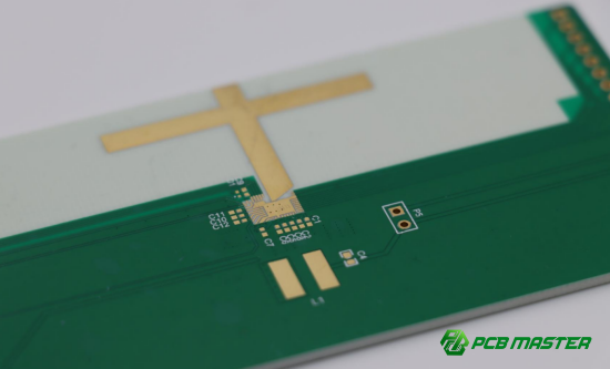
1. BGA solder pads (Ball Grid Array)
ENIG is widely used for BGA pads in PCB manufacturing because it provides a very flat and uniform surface. This ensures strong and reliable solder joints during reflow soldering.
Example: In smartphone processors, BGA pads must be extremely flat to avoid solder voids, making ENIG the standard choice.
For QFN (Quad Flat No-lead) packages , ENIG provides excellent surface planarity and wetting performance, which is critical for small pad sizes.
Example: In IoT sensor chips, QFN packages rely on ENIG to ensure stable solder connection at very fine spacing.
3. High-flatness SMT soldering surfaces
ENIG is preferred for general SMT PCB assembly , especially when high surface flatness is required to avoid solder bridging or uneven joints.
4. COB (Chip-on-Board) wire bonding applications
In COB bonding applications , ENIG provides a stable and clean surface suitable for gold wire bonding due to its controlled surface chemistry.
When should you prefer hard gold plating?
Hard gold plating is preferred when the application requires frequent mechanical contact and wear resistance.
In hard gold PCB surface finish applications , the focus is not soldering, but mechanical durability and electrical contact reliability .
1. Gold fingers (edge connectors)
Hard gold is the standard for PCB gold fingers because it must withstand thousands of insert–remove cycles without wearing out.
Example: Memory cards and SIM cards rely on hard gold plating to maintain stable electrical contact.
2. Plug-in connectors
In PCB connector systems , hard gold ensures low contact resistance and long-term stability under mechanical friction.
3. Key contact points (switches, buttons)
For electronic keypads or contact switches , hard gold provides stable electrical performance even after repeated pressing cycles.
4. Thick gold test fixtures
In testing jigs and probe fixtures , hard gold is used because it can handle repeated mechanical contact without surface degradation.
What is the decision logic for choosing ENIG vs. hard gold?
The selection depends on whether the application prioritizes soldering reliability, mechanical wear resistance, or structural durability.
1. Is soldering the main requirement?
- Yes → Choose ENIG (Electroless Nickel Immersion Gold)
- No → Consider hard gold
ENIG is designed for SMT assembly, BGA, and QFN soldering applications , where the PCB is soldered once and used permanently.
2. Is there frequent mechanical contact or friction?
- Yes → Choose hard gold plating
- No → ENIG is sufficient
Hard gold is designed for repeated insertion, plugging, and mechanical wear environments .
3. Is a thick gold and wear-resistant structure required?
- Yes → Choose hard gold
- No → ENIG is more cost-efficient
Hard gold uses a thicker electroplated gold layer over pure nickel , making it suitable for durability-focused designs.
Simple engineering rule (easy selection guide)
- ENIG = “solder once, stay forever” (assembly-focused)
- Hard gold = “plug many times, still works” (contact-focused)
Practical selection summary (real engineering view)
| Application type | Recommended finish | Reason |
| BGA / QFN / SMT pads | ENIG | Excellent flatness and solderability |
| COB wire bonding | ENIG | Stable surface for bonding |
| Gold fingers | Hard gold | High wear resistance |
| Connectors | Hard gold | Repeated insertion durability |
| Test fixtures | Hard gold | Long-term mechanical contact |
Key takeaway
Choosing between ENIG and hard gold is not about which is “better,” but about matching the surface function to the real working condition: soldering reliability vs . mechanical contact durability .
Is ENIG Suitable for High-Frequency Circuits?
ENIG can be used in many high-frequency circuits, but its nickel layer introduces additional signal loss, so it is generally suitable for lower-to-mid RF applications while requiring careful evaluation or avoidance in high-frequency and millimeter-wave designs.
What are the limitations of ENIG in high-frequency applications?
ENIG is usable in many RF circuits, but its nickel layer can introduce signal loss because nickel is less conductive than copper.
In ENIG PCB surface finish for high-frequency circuits , the main concern is the nickel–phosphorus (Ni-P) layer , which sits between copper and gold. Nickel has a much lower electrical conductivity than copper , so it can slightly disturb signal transmission, especially in RF and microwave designs.
A second limitation is the skin effect (current crowding at high frequency) . At high frequencies, current flows mainly on the surface of the conductor. This means the signal interacts more with the nickel layer instead of deeper copper, increasing loss.
Key impacts in ENIG high-frequency signal loss :
- Slight increase in insertion loss
- Higher signal attenuation at RF frequencies
- Potential phase distortion in sensitive circuits
Example: In a 2.4 GHz Wi-Fi PCB, ENIG is usually acceptable, but engineers may still optimize pad size or avoid unnecessary nickel exposure in critical RF paths.
What should be considered in millimeter-wave (mmWave) applicatio vs ns?
In mmWave designs, even small losses from ENIG become more significant, so its impact must be carefully evaluated based on frequency and stack-up structure.
In ENIG high-frequency mmWave PCB design , the challenge increases as frequency rises above 20–30 GHz. At these frequencies, electromagnetic waves are more sensitive to material changes.
Key considerations:
1. Nickel layer influence becomes more visible
Even a thin Ni-P layer can introduce measurable loss because the signal energy is concentrated near the surface.
2. Loss is amplified at higher frequencies
As frequency increases:
- Skin depth becomes thinner
- Signal interacts more with nickel layer
- Overall transmission loss increases significantly
3. Design must consider full stack-up structure
Engineers must evaluate:
- Copper thickness
- ENIG nickel thickness
- Trace geometry
- Impedance matching requirements
Example: In automotive radar systems (77 GHz), designers often avoid unnecessary ENIG exposure in critical RF signal paths to minimize loss.
How should ENIG be selected for high-frequency PCB design?
Selection should be based on operating frequency, loss tolerance, cost, and reliability requirements.
In high-frequency PCB surface finish selection (ENIG vs . alternatives) , engineers must balance electrical performance and manufacturing practicality.
1. Clearly define operating frequency band
- Below ~6 GHz → ENIG usually acceptable
- 6–30 GHz → careful evaluation required
- Above 30 GHz (mmWave) → strict control or alternative finishes may be preferred
2. Balance signal loss vs . manufacturing cost
ENIG is widely used because it:
- Provides excellent solderability
- Is cost-effective for mass productionBut may introduce:
- Slight RF loss compared to copper-only or specialized finishes
3. Consider reliability and production needs
Even in RF designs, ENIG may still be chosen when:
- SMT assembly reliability is critical
- Fine-pitch components are used
- Long-term corrosion resistance is required
Example: In 5G base station PCBs, ENIG is often used in non-critical RF regions, while sensitive transmission lines may use optimized surface treatments.
Simple engineering takeaway
- ENIG = good general-purpose finish, but not “loss-free” for RF
- High frequency = more sensitivity to nickel effects
- mmWave = requires careful electromagnetic design validation
Key conclusion
ENIG can be used in high-frequency circuits, but in RF and especially mmWave designs, its nickel layer introduces measurable signal loss, so engineers must evaluate frequency, structure, and performance requirements before selection.
ENIG vs. Hard Gold Nickel Layer Difference Summary: How to Quickly Identify Them?
ENIG uses a nickel–phosphorus alloy deposited by a chemical process for soldering applications, while hard gold plating uses pure electroplated nickel for wear-resistant electrical contacts, and they can be quickly distinguished by composition, process, and application area.
How to identify by material composition?
ENIG uses a nickel–phosphorus (Ni-P) alloy, while hard gold plating uses pure nickel.
In ENIG vs . hard gold nickel composition comparison , the fastest way to distinguish the two is by their material structure.
- ENIG (Electroless Nickel Immersion Gold): The nickel layer is a nickel–phosphorus alloy (Ni-P) . Phosphorus is intentionally added during chemical deposition, which changes the structure and properties.
- Hard gold plating: The nickel layer is electroplated pure nickel , with almost no alloying elements.
Simple rule:
- Ni-P alloy = ENIG nickel layer
- Pure nickel = hard gold nickel layer
Example: If a PCB datasheet mentions “medium phosphorus ENIG (6–9%)”, it clearly indicates an ENIG surface finish used for soldering pads.
How to identify by function?
ENIG is used for soldering, while hard gold is used for wear-resistant electrical contact.
In PCB surface finish selection (ENIG vs . hard gold function comparison) , the application purpose is a strong identification clue.
ENIG functional focus: solderability
- Used for SMT assembly
- Designed for BGA and QFN solder joints
- Only needs to support one-time soldering
Hard gold functional focus: durability
- Used for repeated plugging and contact
- Designed for mechanical wear resistance
- Supports thousands of insertion cycles
Example: A smartphone motherboard uses ENIG on chip pads for soldering, while the SIM card edge uses hard gold for repeated insertion.
How to identify by manufacturing process?
ENIG uses chemical (electroless) deposition, while hard gold uses electroplating with electric current.
In ENIG vs . hard gold plating process comparison , the deposition method clearly separates the two technologies.
ENIG process (chemical deposition):
- No external current required
- Nickel and phosphorus deposit together
- Uniform coating even on complex surfaces
Hard gold process (electroplating):
- Requires electric current
- Pure nickel is deposited first, then gold
- Thickness depends on current distribution
Simple distinction rule:
- Chemical reaction → ENIG
- Electric current plating → hard gold
Example: ENIG can coat deep vias evenly, while hard gold plating may show thicker edges due to current concentration.
How to identify by application area?
ENIG is used in SMT soldering areas, while hard gold is used in gold fingers and contact interfaces.
In PCB application-based identification (ENIG vs . hard gold usage areas) , location on the board is often the easiest clue.
ENIG application areas: SMT zones
- BGA pads
- QFN pads
- General soldering surfaces
- Chip bonding areas (COB)
Hard gold application areas: mechanical contact zones
- Gold fingers (edge connectors)
- Plug-in connectors
- Key contacts and switch pads
- Test fixtures
Example: On a laptop motherboard:
- CPU and memory pads → ENIG (soldered once)
- Memory card edge → hard gold (inserted repeatedly)
Key takeaway (quick identification logic)
To quickly distinguish ENIG vs. hard gold nickel layers:
- Composition → Ni-P = ENIG, Pure Ni = hard gold
- Function → soldering = ENIG, wear/contact = hard goldProcess → chemical = ENIG, electroplating = hard gold
- Application → SMT pads = ENIG, connectors = hard gold
This makes it easy to identify ENIG vs . hard gold PCB surface finish differences in real engineering scenarios .
Conclusion
The difference between ENIG and hard gold nickel layers is not just a material variation, but a clear functional division in PCB design. ENIG (nickel–phosphorus alloy) is optimized for reliable soldering, excellent flatness, and fine-pitch SMT applications such as BGA and QFN. In contrast, hard gold plating (pure nickel system) is designed for mechanical durability, stable electrical contact, and long-term wear resistance in applications like gold fingers and connectors.
Therefore, when selecting a surface finish, engineers should always align the choice with real operating conditions—whether the priority is soldering reliability or repeated mechanical contact performance. A correct decision at this stage can significantly improve product yield, stability, and service life.
If you are working on high-reliability PCB or PCBA projects and need professional support in surface finish selection or manufacturing optimization, PCBMASTER, an experienced PCB and PCBA supplier , can provide strong engineering guidance and production capability to help ensure your design performs reliably in real-world applications.
FAQs
Is the ENIG nickel layer pure nickel?
No, the ENIG nickel layer is actually a nickel–phosphorus (Ni-P) alloy, not pure nickel. The phosphorus is co-deposited during the electroless plating process, which changes the structure and makes it different from pure electroplated nickel used in hard gold systems.
Is the nickel layer in hard gold always pure nickel?
In most cases, yes—it is electroplated pure nickel, commonly bright nickel or low-stress matte nickel. These forms are used to ensure good conductivity, mechanical stability, and reliable performance in connector and gold finger applications.
Why is ENIG nickel hardness higher than pure nickel?
Because the nickel–phosphorus alloy structure and phosphorus strengthening effect significantly increase hardness. The amorphous or microcrystalline structure of Ni-P reduces grain boundaries and improves hardness, making ENIG harder than standard pure nickel.
Why can’t gold fingers use ENIG instead of hard gold plating?
Because ENIG does not provide sufficient wear resistance for repeated insertion and long-term mechanical contact. Gold fingers require a durable pure nickel base and thick gold layer to withstand thousands of mating cycles without surface failure.
How can you quickly distinguish ENIG from hard gold plating on a PCB?
You can identify them by location, process description, and usage pattern.
- SMT solder pads → usually ENIG
- Gold finger or connector areas → usually hard gold plating
- ENIG is chemical deposition, while hard gold is electroplated with pure nickel underneath
About the Author

Carol Luo
PCB Design EngineerI'm Carol, a PCB Engineer at PCBMASTER with experience in PCB design and manufacturing engineering since 2018. I focus on translating engineering requirements into reliable PCB solutions, with expertise in stack-up design, material selection, and design-for-manufacturing (DFM). I share practical engineering insights from real-world PCB design and production experience.
Visit Carol Luo's Profile
