Unveiling the Magic of PCB Via Filled with Copper&Silver
Introduction
In the intricate world of Printed Circuit Boards (PCBs), every component and process plays a pivotal role in determining the board's performance. One such crucial process is via filling, and when it comes to using conductive materials like copper and silver for this task, the results can be game - changing. This blog will take you on a journey through the realm of PCB vias filled with copper and silver, exploring what it is, why it's important, and how it impacts the overall functionality of PCBs.
What are PCB Vias?

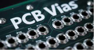
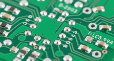
Before diving into the details of copper/silver-filled vias, let’s first understand what vias are in the context of PCBs. A via is a small hole drilled through the layers of a PCB. Its primary function is to create an electrical connection between one PCB layer and another, enabling electrical connections across multiple PCB layers. There are various types of vias, such as through-hole vias (also called through holes) that pass through the entire thickness of the PCB, microvias which are extremely small vias often used in high-density interconnect (HDI) boards, blind vias that connect the outer layers to an inner layer but don’t go all the way through, and buried vias that are hidden between inner layers.
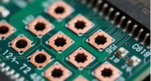
Normally, during the PCB manufacturing process, the hole walls of vias are first plated with copper, creating a copper plated hole. This copper plating forms essential copper features within the via structure and is crucial for ensuring proper electrical conductivity. However, in some cases, just this initial plating isn’t enough, and that’s where via filling comes into play.
The Concept of Via Filling
Via filling is exactly what it sounds like—the process of filling these drilled holes with a particular material. Via fill is a pcb manufacturing technique used to create a completely filled via for improved reliability and performance. The filling material, or fill material, can be either conductive or non-conductive, depending on the requirements of the PCB design and the intended function of the via. Common filling materials include epoxy resin, copper paste, silver epoxy, and conductive epoxy; the choice of fill material affects the via's electrical, thermal, and mechanical properties and must be compatible with the surrounding laminate.
Non conductive materials, such as non conductive epoxy, non conductive epoxy material, or non conductive paste, are used for non conductive filling to provide structural support, seal vias, and prevent contamination. This type of non conductive material is essential for applications where electrical insulation and reliability are required. Resin plugging is another pcb fabrication method for filling vias, though it may not result in a completely filled via.
When a via is filled with a conductive material, such as copper conductive epoxy, silver epoxy, copper paste, or other conductive fillings, it creates conductive filled vias that offer enhanced electrical and thermal performance. Conductive fillings are used to ensure a solid electrical connection between the layers, which is especially important in high-density PCB designs where signal integrity, heat dissipation, and reliability are of utmost importance. This is in contrast to a non-filled or just-plated via, which may have some air gaps or be more prone to issues like signal interference or poor thermal management.
Copper - Filled Vias

Why Copper?
Copper is by far the most commonly used material for conductive via filling in PCBs. There are several reasons for its popularity:
Excellent Electrical Conductivity
Copper has an outstanding electrical conductivity, with a value of approximately 5.96 x 10^7 S/m. This high conductivity allows electrical signals to pass through the vias with minimal resistance. In high - speed applications, such as those found in modern computers, servers, and telecommunications equipment, minimizing signal loss is crucial. Copper - filled vias ensure that signals can travel between different layers of the PCB seamlessly, maintaining their integrity and strength. For example, in a high - performance graphics card, where data needs to be transferred rapidly between various components on different layers of the PCB, copper - filled vias help in ensuring that the graphics processing unit (GPU) can communicate efficiently with the memory modules.
Good Thermal Conductivity
In addition to its electrical properties, copper also has excellent thermal conductivity, measuring around 401 W/m·K. This makes it a great choice for dissipating heat in PCBs. In high - power applications, components like CPUs, GPUs, and power transistors generate a significant amount of heat. If this heat isn't properly managed, it can lead to component failure and reduced lifespan of the PCB. Copper - filled vias act as thermal pathways, helping to transfer heat away from these hot components to other parts of the PCB or to external heat sinks. In a laptop's motherboard, copper - filled vias assist in moving the heat generated by the CPU and other components to the heat pipes and ultimately to the cooling fan, keeping the system from overheating.
Cost - Effectiveness
Compared to some other conductive materials, copper is relatively cost-effective. While there are more exotic materials with even better electrical or thermal properties, they often come at a much higher price. Copper provides an excellent balance between performance and cost, making it the go-to choice for most PCB manufacturers. This cost-effectiveness also extends to the manufacturing process. The equipment and techniques required for copper electroplating (the most common method for filling vias with copper) are widely available and well-established in the industry, further reducing production costs.
The filling cost of copper filled vias is influenced by several factors, including the type of filling material used and the layer count of the PCB. Higher layer counts increase the complexity of the via filling process, as they require more precise layer-to-layer alignment and via precision, which can significantly impact the overall filling cost, especially in multilayer or HDI boards.
The Copper Via - Filling Process
The process of filling vias with copper typically involves the following steps:
Drilling and Plating
First, vias are drilled into the PCB, with careful control of hole depth to ensure proper aspect ratio and reliable electrical connections. During the plating process, copper is deposited onto the hole barrel, which is the internal surface of the drilled via, to establish electrical conductivity.
Filling
After plating, the vias are filled with a conductive or non-conductive resin. It is crucial to eliminate trapped air within the via during this step, as trapped air can cause reliability issues, failures during assembly, and reduce the lifespan of the circuit board.
Planarization
Once the resin is cured, planarization is performed to remove any excess resin and achieve a flat surface and uniform surface. This step is essential for preparing the PCB for subsequent manufacturing processes, such as over-plating and component soldering.
Electroless Copper Deposition
The first step is to deposit a thin layer of copper onto the walls of the drilled holes. This is done through electroless copper deposition. In this process, a chemical solution is used to deposit copper onto the non - conductive surface of the hole walls. The solution contains copper ions and reducing agents. When the solution comes into contact with the hole walls, a chemical reaction occurs, and copper ions are reduced to metallic copper and deposited on the surface. This initial layer of copper serves as a base for the subsequent electroplating process.
Electroplating
Once the electroless copper layer is in place, electroplating is used to build up the thickness of the copper in the vias. During electroplating, the PCB is placed in an electrolyte solution containing copper ions. A direct current is applied, with the PCB acting as the cathode and a copper anode in the solution. The copper ions in the solution are attracted to the negatively charged PCB, and they deposit onto the existing copper layer in the vias, gradually filling them up. This process allows for precise control over the thickness of the copper fill, ensuring that the vias have the desired electrical and thermal properties.
Planarization
After the vias are filled with copper, the surface of the PCB may have some excess copper. Planarization is the process of flattening the surface of the PCB to remove this excess copper. This can be done through methods such as mechanical polishing or chemical - mechanical planarization (CMP). Planarization is important as it ensures that the surface of the PCB is smooth and flat, which is necessary for subsequent processes like soldering components onto the board. It also helps in preventing short circuits that could occur if the excess copper were left protruding from the surface.
Silver - Filled Vias

Why Silver?
Silver is another option for conductive via filling, although it is less commonly used compared to copper. However, it offers some unique advantages that make it suitable for certain applications:
Higher Electrical Conductivity than Copper
Silver has an even higher electrical conductivity than copper, with a value of around 6.30 x 10^7 S/m. This means that in applications where extremely low resistance and maximum signal transfer efficiency are required, silver - filled vias can provide a performance edge. For example, in high - frequency communication systems such as satellite communication equipment or some high - end medical imaging devices, the use of silver - filled vias can help in minimizing signal attenuation and distortion, ensuring clear and accurate data transmission.
Excellent Thermal Conductivity
Similar to copper, silver also has good thermal conductivity, measuring around 429 W/m·K. This makes it effective in dissipating heat, which is beneficial in high - power applications. In some high - performance computing applications where heat management is critical, silver - filled vias can be used to enhance the thermal performance of the PCB, allowing components to operate at lower temperatures and with higher reliability.
Resistance to Oxidation and Corrosion
Silver has better resistance to oxidation and corrosion compared to some other metals. This is important as it helps in maintaining the integrity of the electrical connection over time. In environments where the PCB may be exposed to moisture, chemicals, or other corrosive substances, silver - filled vias are less likely to degrade and cause electrical problems. For example, in PCB designs for marine electronics or industrial control systems that may be used in harsh environments, the use of silver - filled vias can improve the long - term reliability of the board.
Drawbacks of Silver - Filled Vias
Despite its advantages, silver-filled vias also have some drawbacks. The main one is the cost. Silver is more expensive than copper, and this higher cost is reflected in the manufacturing process. The filling cost of silver-filled vias is significantly higher than copper due to the expense of the silver material and the specialized processes required for via filling. This higher filling cost can make PCB production significantly more expensive. As a result, the use of silver-filled vias is typically limited to applications where the performance benefits justify the additional expense, such as in high-end military or aerospace electronics.
Applications of Copper/Silver - Filled Vias
High - Density Interconnect (HDI) Boards
In HDI boards, where components are packed closely together and there is a high demand for efficient signal routing, copper/silver-filled vias are essential. HDI designs often require completely filled vias to ensure reliability and prevent contamination. Filled and capped vias, including capped vias and via in pads, are advanced solutions used in HDI boards to create shorter signal paths and support higher component density. The via in pad process involves filling, planarizing, and plating the via directly under the pad, with the active pad playing a key role in improving signal transmission and reducing solder bridging. These boards are used in a wide range of applications, from smartphones and tablets to high-performance servers. The use of filled vias helps in reducing signal interference and improving signal integrity in these densely populated boards. In a smartphone’s motherboard, which contains numerous components such as the processor, memory, and various sensors, copper-filled vias enable the quick and reliable transfer of data between different layers, ensuring smooth operation of the device.
High - Power Applications
For high - power applications like power supplies, electric vehicle chargers, and industrial motors, heat management is a major concern. Copper/silver - filled vias play a crucial role in dissipating the heat generated by the high - power components. In an electric vehicle charger, where large amounts of electrical power are being converted and transferred, copper - filled vias help in channeling the heat away from the power - handling components to the heat sink, preventing overheating and ensuring the safe and efficient operation of the charger.
High - Frequency Applications
In high - frequency applications such as 5G base stations, radar systems, and wireless communication devices, signal integrity is of utmost importance. Copper/silver - filled vias, with their excellent electrical conductivity, help in minimizing signal loss and distortion. In a 5G base station, which operates at high frequencies and requires rapid data transfer, silver - filled vias (if the cost - performance ratio allows) can be used to ensure that the signals transmitted between different parts of the PCB maintain their strength and integrity, enabling seamless communication.
The Impact on PCB Performance

Improved Electrical Conductivity
As mentioned earlier, copper and silver - filled vias provide a low - resistance path for electrical signals. This leads to improved electrical conductivity, which is essential for the proper functioning of PCBs. Minimizing signal loss means that components on different layers of the PCB can communicate more effectively. In a complex PCB with multiple integrated circuits and other components, efficient signal transfer via copper/silver - filled vias ensures that data can be processed and transmitted without errors or delays.
Enhanced Signal Integrity
By creating a solid conductive path, filled vias reduce the risk of signal reflections and distortions. In high - speed digital circuits, signal integrity is crucial. Any interference or distortion in the signal can lead to data errors and malfunctions. Copper/silver - filled vias act as a reliable conduit for signals, ensuring that they reach their destination in the correct form. This is particularly important in applications like high - speed data transfer interfaces, where a single bit error can cause significant problems.
Increased Current Carrying Capacity
Compared to non - filled vias, copper/silver - filled vias have a higher current carrying capacity. This is beneficial in applications where large amounts of current need to be transmitted, such as in power - intensive components. In a power amplifier circuit, which requires a high current to drive the output stage, copper - filled vias can handle the current flow without overheating or experiencing voltage drops, ensuring efficient power delivery.
Better Thermal Management
The good thermal conductivity of copper and silver helps in dissipating heat more efficiently. In PCBs with high - power components, heat can build up quickly and cause performance degradation or component failure. Copper/silver - filled vias act as thermal bridges, spreading the heat across the PCB and allowing it to be dissipated more effectively. This helps in maintaining the operating temperature of the components within a safe range, improving the overall reliability and lifespan of the PCB.
Conclusion
In conclusion, the use of copper and silver for filling vias in PCBs is a technology that has a profound impact on the performance and functionality of these essential electronic components. Copper, with its excellent balance of electrical conductivity, thermal conductivity, and cost - effectiveness, is the workhorse of the industry, finding widespread use in a vast array of applications. Silver, on the other hand, offers superior electrical conductivity and corrosion resistance, making it a viable option for high - end applications where performance trumps cost.
Whether it's improving electrical conductivity, enhancing signal integrity, increasing current carrying capacity, or better managing heat, copper/silver - filled vias play a crucial role in meeting the demands of modern PCB designs. As technology continues to advance, and as the need for smaller, faster, and more efficient electronic devices grows, the importance of these conductive via - filling materials will only increase. PCB designers and manufacturers will continue to rely on copper and silver - filled vias to create the next generation of high - performance printed circuit boards that power our digital world.
Why PCBMASTER: https://www.pcbmaster.com/why
Join US:https://www.pcbmaster.com/login

