


Core Role of Electronic Circuit Board Testing in the Full Lifecycle of PCBA
In the design and production system of PCBA (Printed Circuit Board Assembly), electronic circuit board testing serves as the core quality control process throughout the entire workflow. It encompasses proactive validation during the design phase, real-time defect detection in manufacturing, and functional reliability verification in complex application scenarios. Its significance continues to grow amid technological iteration and industrial upgrades.

I. Design Phase: Test Point Planning and IC Testing Synergy
At the initial design stage of PCBA, testing strategies must align with circuit validation and IC testing compatibility. For ICs with BGA (Ball Grid Array) packaging, test points must be reserved along signal transmission paths to ensure subsequent IC testing feasibility. For example, in a 5G base station motherboard design, engineers placed 256 test points on a 28-layer PCB, with 38% dedicated to boundary scan testing (JTAG interface) for FPGA and RFIC chips, achieving dual verification of chip-level functionality and board-level signal integrity.
Technological Breakthrough: Embedded Test Bus (ETB) technology integrates IC testing interfaces with PCBA test points, improving chip parameter testing efficiency by 70%. A case study on an industrial control board showed that this approach increased IC test coverage from 82% to 99.6%.
II. Production Phase: Multi-Dimensional PCBA and IC Testing Quality Control
On SMT (Surface Mount Technology) production lines, PCBA testing and IC testing form a multi-layered quality assurance system:
1. Surface Defect Screening
① 3D-AOI systems detect 0201 component placement via multi-angle imaging (resolution ≤3μm).
② Custom algorithms identify pin coplanarity for QFN-packaged ICs (tolerance ±15μm).
2. Internal Defect Diagnosis
① CT-X-ray performs 3D reconstruction of BGA-packaged ICs to measure solder ball collapse height (threshold ≥80% ball diameter).
② Microwave probe technology tests impedance of IC power networks (accuracy ±2%).
3. In-Line Functional Validation
① PXI-based platforms synchronize PCBA functional testing with IC parameter testing.
② An automotive ECU production case reduced single-board testing time from 120s to 45s by integrating IC test programs.
Data Support: After adopting collaborative testing solutions, a consumer electronics manufacturer improved PCBA yield rate from 91.2% to 98.5%, while reducing IC testing false rejection rates to 0.03%.
III. Functional Validation: System-Level PCBA-IC Collaboration
At the product validation stage, PCBA testing and IC testing are deeply integrated:
1. Dynamic Parameter Validation
① Real-time power analyzers monitor IC power rail ripple (e.g., DDR5 memory controller requires <20mVpp).
② Temperature cycling tests (-40°C~125°C) validate thermal compatibility between ICs and PCBA.
2. Signal Integrity Testing
① Protocol-level testing for high-speed SerDes interfaces (112Gbps) verifies IC PHY layer and PCB transmission line performance.
② Optimizing IC driver configurations reduced PCBA bit error rates by two orders of magnitude in server motherboard tests.
3. Reliability Validation
① Combined IC aging tests (HTOL) and PCBA vibration tests (20–2000Hz/5Grms).
② A new energy vehicle case accurately predicted system MTBF by correlating IC junction temperature monitoring with PCBA thermal imaging.
IV. Technological Breakthroughs: AI-Driven Testing Evolution
To address challenges from 01005 components and 3D-packaged ICs, innovations include:
1. Virtual Probing Technology
①Non-contact testing for 0.2mm-pitch BGAs using electromagnetic field inversion.
②A millimeter-wave IC test case reconstructed radiation patterns of 128 antenna units via near-field scanning.
2. Deep Learning-Based Inspection
Defect recognition models (ResNet-50 architecture) trained on 120 million X-ray images achieve 99.8% classification accuracy for PCBA and IC defects.
3. Digital Twin Testing
①IC-PCBA co-simulation models predict signal integrity issues upfront.
②A space project reduced physical validation cycles by 68% using virtual testing.
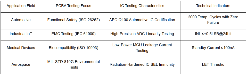
V. Industry Applications: Customized PCBA and IC Testing Solutions
Conclusion
Building a Collaborative PCBA-IC Testing Ecosystem
From wafer-level IC testing to system-level PCBA validation, modern electronics manufacturing relies on deeply integrated testing systems. By correlating IC test data (e.g., WAT parameters) with PCBA test results (e.g., ICT data), root-cause defect analysis becomes precise. A storage server manufacturer reduced early product failure rates by 92% through this synergy, underscoring testing technology’s strategic role as a core competency in the electronics industry.
Author: Jack Wang

