Engineering Guide for High-Frequency FPC Materials Tackling High-Frequency Challenges in Flexible Circuits
Driven by 5G communications, millimeter-wave radar, and high-speed data transmission, high-frequency FPC (Flexible Printed Circuit) has become an indispensable neural pathway for cutting-edge electronic equipment. Unlike traditional FPC materials, high-frequency applications impose near-harsh requirements on the substrate: every inch of signal transmission involves a struggle against the dissipation factor (Df) and the stability of the dielectric constant (Dk). This article will delve into the core engineering points for material selection and design of high-frequency FPC.

I. Core Performance Parameters of High-Frequency FPC Materials:
1. Extremely Low Dissipation Factor (Df): This is the key indicator measuring how much electromagnetic energy a material converts into heat. At high frequencies, even minor losses are dramatically amplified:
Typical Standard PI (Polyimide): Df ≈ 0.008 - 0.012 @ 10 GHz (Loss too high, difficult to meet high-frequency requirements).
High-Frequency FPC Material Representatives:
① Modified Polyimide (MPI): Df ≈ 0.002 - 0.005 @ 10 GHz (e.g., DuPont Pyralux AP, Shengyi Tech SIF-F650).
② Liquid Crystal Polymer (LCP): Df ≈ 0.002 - 0.004 @ 10 GHz (e.g., LCP films from Murata Manufacturing, Kuraray).
③ Polytetrafluoroethylene Composites (PTFE): Df ≈ 0.001 - 0.003 @ 10 GHz (e.g., Rogers RO3000 series laminates, often combined with PI for rigid-flex boards).
2. Stable Dielectric Constant (Dk): The stability of Dk directly affects signal transmission speed (Z0) and phase consistency. Small Dk fluctuations at high frequencies can cause severe signal distortion.
Standard PI: Dk ≈ 3.2 - 3.5, varies significantly with frequency/temperature/humidity.
High-Frequency FPC Material Advantages:
① LCP: Dk ≈ 2.9 - 3.2, excellent frequency/temperature stability (variation rate < 1%).
② PTFE Composites: Dk is designable (e.g., 2.2 - 10.2), with excellent stability.
③ MPI: Dk ≈ 3.0 - 3.8, stability superior to standard PI.
3. Outstanding Temperature and Humidity Stability: Changes in Dk/Df, dimensional stability (CTE), and moisture absorption rate of the material under high temperature and humidity environments directly impact long-term circuit reliability.
Moisture Absorption Rate Comparison:
① Standard PI: ~ 1.8% - 3.0% (High absorption causes significant increase in Dk/Df).
② LCP: ~ 0.02% - 0.10% (Ultra-low absorption).
③ PTFE: ~ < 0.01% (Extremely low absorption).
④ MPI: ~ 0.4% - 1.5% (Better than standard PI).
4. Fine Copper Foil Surface Treatment: High-frequency signals exhibit a significant "skin effect," concentrating current on the conductor surface. Copper foil surface roughness (Rz) becomes critical:
① Standard Electrodeposited Copper (ED): Rz ≈ 3 - 6 μm (Causes additional conductor loss).
② High-Frequency FPC Dedicated Copper Foils:
Very Low Profile/Reverse Treated Foil (VLP/RTF): Rz ≈ 1.5 - 2.5 μm.
Rolled Annealed Copper (RA): Rz ≈ 0.3 - 0.8 μm (Lowest loss, but higher cost, slightly inferior processability).
Table: Key Substrate Performance Comparison for High-Frequency FPC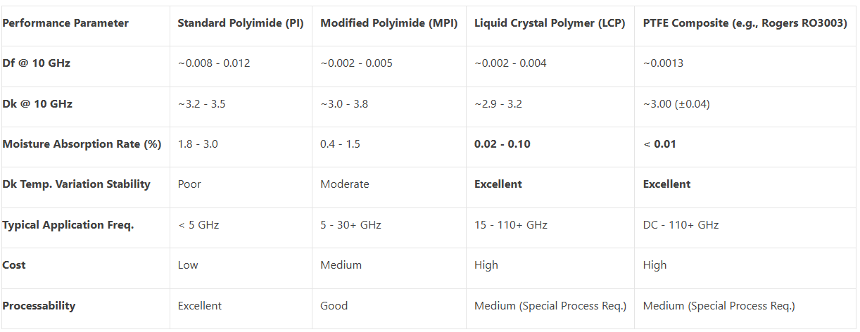
II. Key Engineering Practices for High-Frequency FPC Design
1. Precise Impedance Control:
① Utilize electromagnetic field simulation software (e.g., ADS, HFSS) for modeling, fully considering the Dk value, thickness tolerance, copper thickness/roughness of the FPC materials.
② Strictly control trace width/spacing tolerance: Micron-level deviations at high frequencies lead to significant impedance shifts. Typically requires tolerance within ±10%.
③ Reference Plane Design: Ensure a complete, low-impedance reference plane (usually GND), avoid crossing splits; this is fundamental for controlling impedance and reducing crosstalk.
2. Minimizing Transmission Loss:
① Material Selection is Fundamental: Prioritize high-frequency FPC materials with low Df and low roughness copper foil.
② Optimize Trace Geometry: Within the constraints of current carrying capacity and process capability, appropriately increasing trace width can effectively reduce conductor loss (skin effect impact decreases).
③ Reduce Bends and Vias: Unavoidable bends require large-radius designs; vias are impedance discontinuities and loss sources, minimize their use. Optimize with back-drilling or via filling when necessary.
3. Suppressing Signal Integrity Issues:
① Crosstalk Control: Increase trace spacing (≥3x trace width), use ground traces for shielding critical signal lines.
② Reflection Suppression: Strict impedance control is fundamental; optimize termination matching strategies (source/end resistors).
③ Power Integrity: Design a low-impedance Power Distribution Network (PDN), use bypass/decoupling capacitors, consider power plane design in the FPC stackup.
III. Structural Design and Manufacturing Process Considerations:
① Stackup Structure: Reasonably plan signal layers, reference layers, and shielding layers. Multi-layer high-frequency FPC requires special attention to inter-layer alignment accuracy and lamination process control.
② Coverlay / Shielding Layers: Select Coverlay with low Dk/Df. Electromagnetic shielding layers (e.g., conductive silver paste, copper foil shielding) must be well-grounded to avoid introducing additional loss or resonance.
③ Fine-Line Processing: High-frequency signal trace width/spacing is often less than 50μm, requiring advanced imaging (e.g., LDI Laser Direct Imaging) and etching processes.
④ Low-Loss Soldering/Connections: Choose solder paste and connectors with low dielectric constant and low loss to ensure good impedance matching at connection points.
IV. High-Frequency FPC Material Selection and Cost-Balancing Strategies
1. Sub-6GHz / Cost-Sensitive Applications (e.g., internal smartphone antennas, mid-frequency modules): Modified Polyimide (MPI) is the optimal balance, offering significantly better high-frequency performance than standard PI (lower/more stable Df/Dk, lower moisture absorption), while maintaining good processability and cost controllability.
2. Millimeter-Wave Band / Ultra-High Performance Requirements (e.g., 5G mmWave antennas, automotive radar, high-speed data connectors): Liquid Crystal Polymer (LCP) is the undisputed king, thanks to its ultra-low and extremely stable Df/Dk and near-zero water absorption. PTFE composites are strong candidates for rigid-flex boards or specific ultra-wideband designs. However, LCP and PTFE have high raw material costs, difficult processing (especially multi-layer lamination), significant yield challenges, resulting in the highest total cost.
3. Emerging Options - Low-Loss Thermoset Materials: Some new thermoset resins (e.g., modified BT, PPE materials) are under development, aiming to provide performance close to LCP but with better processability and cost potential. This is a direction worth watching.
V. Application Case Sidebar: High-Frequency FPC Materials in Action
1. 5G Smartphone Millimeter-Wave Antenna Module: Utilizes multi-layer LCP-based high-frequency FPC to achieve precise transmission and reception of 28GHz/39GHz signals in an ultra-thin form factor. Df<0.003 ensures antenna efficiency >65%.
2. 77GHz Automotive Radar Sensor: Flexible transmission lines made from MPI or LCP FPC materials conduct radar chip signals with low loss (<0.3dB/cm) to the onboard antenna array, enduring -40℃ to 125℃ environmental tests.
3. 100G+ Optical Module Internal Interconnect: High-frequency FPC using ultra-low roughness rolled annealed copper (RA) combined with modified PI substrate carries 112Gbps PAM4 signals, with insertion loss <0.8dB/inch @ 28GHz.
4. Phased Array Satellite Communication Terminal: PTFE composite high-frequency FPC materials used in large curved arrays ensure beam pointing accuracy of 0.1° through Dk stability (±0.05), adapting to high-altitude temperature variations.
VI. Process Essentials: Special Requirements for High-Frequency FPC
1. Laser Direct Imaging (LDI): Essential technology to achieve ≤20μm line accuracy (traditional exposure accuracy ~50μm).
2. Plasma Treatment: LCP/PTFE surfaces require activation before lamination; dyne level needs >50mN/m.
3. Low-Temperature Lamination Process: LCP multi-layer board lamination temperature needs controlled at 280±5°C (traditional PI is 350°C+).
4. Impedance Testing: Must use Vector Network Analyzer (VNA) for 10% sampling tests, tolerance ±7Ω (typical 50Ω system).
Conclusion: The Precise Trade-off Between Performance, Process, and Cost
The design and manufacturing of high-frequency FPC is a precision engineering task seeking the optimal balance point between electrical performance, mechanical reliability, thermal management, and cost. A deep understanding of the core parameters (Df, Dk, moisture absorption rate, copper foil roughness) of different high-frequency FPC materials (MPI, LCP, PTFE composites) and their impact on system performance is the foundation of success. Designers must closely integrate material properties, utilize precise simulation tools, and enforce strict process controls to master the complex journey of millimeter-wave signals on flexible substrates.
With the development of 5G-Advanced, 6G, autonomous driving, and next-generation consumer electronics, the performance requirements for high-frequency FPC will continue to increase. Continuous material innovation (e.g., new polymers with even lower loss, smoother copper foil technologies) and more precise manufacturing processes (e.g., ultra-fine lines, high-precision multi-layer lamination) will be the core drivers pushing breakthroughs in this critical field. For engineers, mastering this Engineering Guide for High-Frequency FPC Materials is the key to unlocking the future world of high-speed wireless connectivity.