


Flexible Printed Circuit (FPC) Assembly The Critical Enabler for Next-Generation Electronics
In the relentless pursuit of ultra-thin, foldable, and highly integrated electronic devices, FPC assembly(Flexible Printed Circuit)technology plays a pivotal role. It acts as the "flexible neural network" of electronics, enabling intricate connections within confined spaces and under dynamic bending. This article delves into the core technical challenges of FPC assembly, its breakthrough applications, and exciting future directions.
I. FPC Assembly – Linking SMT Process Capabilities: Key Technical Points & Core Challenges
FPC assembly refers to the process of applying Surface Mount Technology (SMT) onto flexible printed circuits. Its core difficulty lies in achieving reliable assembly of precision electronic components – with requirements matching or exceeding those for rigid PCBs – onto a soft, easily deformable substrate with limited heat tolerance.
1.Precision Positioning & Dynamic Compensation:
①Challenge Root Cause: FPC substrates (e.g., Polyimide PI, typically 0.1-0.3mm thick) are highly susceptible to stretching, twisting (Z-axis warpage up to 1-3mm), or shifting during SMT conveyance and heating.
②Key Technologies:
High-Precision Vision Systems: Rely on advanced machine vision (pre-AOI) to capture FPC fiducial marks in real-time, requiring accuracy typically within ±0.05mm.
Dynamic Compensation Algorithms: Placement machines must possess real-time calculation and compensation capabilities for coordinate shifts caused by FPC deformation, ensuring precise placement of components (especially 0201/01005 micro-components, fine-pitch BGA/QFN).
Critical Data: High-end SMT equipment now demands FPC placement accuracy of ±0.025mm (Cpk > 1.33), far exceeding the ±0.05mm standard for standard rigid boards.
2.Stable Support & Fixture Design:
①Challenge Root Cause: The flexible substrate lacks inherent support during placement and reflow soldering, making it highly prone to deformation under thermal stress, leading to soldering defects.
②Key Technologies:
Dedicated Carriers/Fixtures (Jigs): Utilize precision-designed vacuum suction or magnetic carriers/pallets to provide rigid support throughout production and soldering. Fixtures must perfectly match the FPC contour, accommodating connector clearances and potential bend areas.
Material Selection: Fixtures require excellent dimensional stability, high-temperature resistance (withstanding >260°C), and a low Coefficient of Thermal Expansion (CTE).
Critical Role: Effectively suppresses FPC deformation within the reflow peak temperature zone (typically 220-245°C), ensuring solder joint quality.
3.Low-Temperature Soldering Process: Fine Control to Avoid "Burning":
①Challenge Root Cause: PI substrates have a maximum temperature tolerance of ~250-350°C, significantly lower than FR4 (>280°C easily). Excessive temperature or prolonged reflow time readily causes substrate blistering, delamination, discoloration (yellowing), or carbonization failure.
②Key Technologies:
Low-Temperature Solder Selection: Predominant use includes low-temperature alloys derived from SAC305 (e.g., SAC0307-M, melting point ~217°C) or SnBi-based alloys (e.g., Sn42Bi58, melting point ~138°C; SnBiAg). Demand for lead-free low-temperature solder paste (melting point <200°C) is surging.
Precise Thermal Profile Optimization: Strict control of preheat ramp rate, peak temperature (typically set within a narrow window of 200-230°C), and Time Above Liquidus (TAL) is essential to avoid thermal shock. Requires excellent reflow oven zone uniformity (within ±2°C).
Solder Joint Reliability Design: Employ teardrop pads, anchor holes, coverlay (CVL) opening optimization, etc., to mitigate thermomechanical stress fatigue caused by CTE mismatch between the flexible substrate and copper foil/components.
Critical Data: When using SnBi solder, peak temperature must be strictly controlled within 170-190°C, with TAL often compressed to 30-60 seconds.
4.3D Assembly & Reliability Design: Anticipating Bend "Intelligence":
①Challenge Root Cause: The core value of FPCs lies in bending and dynamic applications. Component placement, routing, and solder joints must maintain long-term reliability in the final assembled form (bent, folded).
②Key Technologies:
Dynamic Bend Design: Precisely calculate minimum bend radius (Dynamic applications: R > 100T, T=total thickness; Static applications: R > 10T). E.g., a 0.2mm thick FPC in a hinge requires a dynamic bend radius >20mm. Critical components are placed away from high-stress bend zones.
Stackup & Routing Optimization: Multi-layer FPCs (up to 20+ layers) utilize staggered routing and rounded corners to reduce stress concentration. Shielding layer design must consider bendability.
Simulation-Driven Design: Leverage FEA (Finite Element Analysis) tools to simulate stress distribution under bending/twisting states, predicting solder joint and trace fatigue life (target bend cycles: 100k-200k+).
Connector Selection: Choose connectors with low insertion force, high durability, and suitability for dynamic bending.
II.FPC Assembly Breakthrough Applications:
1.Foldable/Rollable Display Devices – Linking Product Centers:

①Core Role: Within the extremely confined hinge space, multi-layer stacked or intricately routed FPCs are the only viable solution for connecting the display to the mainboard, enduring dozens of open/close bends daily.
②Data Support: FPCs in mainstream foldable phones (e.g., Samsung Galaxy Z Fold 5, Huawei Mate X3) commonly feature bend radii <3mm within the hinge, with bend cycle testing requirements >200k. DSCC forecasts foldable phone shipments will exceed 30 million units by 2025, driving significant FPC demand growth.
2. High-End TWS Earbuds & Wearables:

①Core Role: Efficiently connects the main SoC, battery, multiple microphones, sensors, and touch areas within the compact cavity of devices like AirPods Pro, conforming perfectly to complex curves. Connects displays, sensor modules, and mainboards in smartwatches/bands.
②Data Support: A single high-end TWS earbud typically integrates 3-5 distinct FPC assemblies. Global TWS shipments exceed 300 million units annually (Canalys 2023), and smartwatch shipments surpass 150 million units (IDC 2023), representing core markets for FPC assembly technology.
3. Automotive Electronics: The Vehicle's "Flexible Neural Network":

Core Role:
Smart Cockpit: Connects driver ICs for large/curved center displays, instrument clusters, and HUDs, enabling narrow bezels.
Sensor Interconnect: Provides flexible wiring within and between ADAS cameras (especially surround-view systems), mmWave radar, and LiDAR modules, adapting to varied mounting angles.
Body Control: Replaces traditional wiring harnesses in door modules (window, speaker, ambient light control), seat adjustment, steering wheel controls.
Battery Management (BMS): High-density FPCs used as voltage/temperature sensing harnesses within New Energy Vehicle (NEV) battery packs (hundreds of sensing points), offering advantages in reliability, weight reduction, and automated production.
4. Advanced Medical Electronics: Precision Connection in Confined Spaces:

Core Role:
Minimally Invasive Devices: In electronic endoscopes (especially ultra-slim scopes <3mm diameter), FPCs are the sole pathway connecting imaging sensors (CMOS/CCD) to external processing units, transmitting HD image signals.
Wearable/Implantable Monitoring: Continuous Glucose Monitors (CGM), cardiac monitoring patches rely on flexible FPCs (often using biocompatible materials/coatings) for comfortable, long-term, stable surface biopotential acquisition.
Micro-Surgical Robots: Transmit high-precision control signals and force feedback sensory signals within dexterous manipulator joints.
High Reliability: Medical devices impose extremely stringent requirements on FPCs for long-term stability, signal integrity, and biocompatibility.
Stringent Requirements: Automotive-grade FPCs must meet AEC-Q100/200 certification, withstand temperatures from -40°C to 125°C (locally 150°C), and exhibit high vibration resistance and chemical corrosion resistance. FPC usage per vehicle is growing rapidly.
III. FPC Assembly Future Trends: Thinner, Denser, Smarter, More Integrated

FPC assembly technology continues to evolve rapidly, with future development focused on key directions:
1.Extreme Miniaturization & Ultra-High Density Interconnect (UHDI):
①Line Width/Space (L/S) Shrinking: Progressing from the current mainstream 35μm/35μm towards 25μm/25μm and even 15μm/15μm and below, meeting high-speed chip-to-chip interconnect demands.
②Ultra-Thin Material Adoption: Use of <5μm ultra-thin copper foil, thinner coverlay (CVL), and substrates (PI/PET <25μm), enabling overall thicknesses <0.1mm.
③Advanced Packaging Integration: Fan-Out Wafer Level Packaging (Fan-Out WLP) and System-in-Package (SiP) directly integrated with FPCs, achieving chip-scale high-density 3D integration on flexible substrates.
2.Material Innovation: Dual Evolution of Performance & Sustainability:
①High-Performance Substrates: Liquid Crystal Polymer (LCP), with ultra-low moisture absorption, excellent high-frequency properties (low Dk/Df), and high dimensional stability, is progressively replacing traditional PI in 5G/mmWave antennas and high-frequency interconnects. Modified PI, Polyethylene Naphthalate (PEN), and Thermoplastic Polyimide (TPI) are also expanding applications.
②Stretchable Electronics: Exploration of liquid metals (Gallium-based alloys), conductive polymer composites, serpentine/fractal metal traces to grant FPCs true elastic stretchability (strain >20%), applicable in e-skin, biomimetic robots, and highly conformable wearables.
③Green & Sustainable: Development of bio-based, recyclable, biodegradable substrates (e.g., cellulose nanofiber-based) to reduce e-waste pollution.
3.Process Intelligence & Reliability Leap:
①AI-Powered SMT: Utilize machine vision + deep learning for real-time FPC deformation prediction, 3D solder paste inspection (SPI), automatic placement offset compensation, and dynamic thermal profile optimization, boosting yield and efficiency.
②Digital Twin & Simulation: Physics-based and big-data reliability simulation (thermal, mechanical stress, fatigue life) predicts product performance during design, accelerating development iteration.
③High-Frequency/High-Speed Design Optimization: For 5G/6G and high-speed data (e.g., USB4, PCIe Gen5), develop more precise impedance control tools and SI/PI (Signal/Power Integrity) co-simulation solutions to address signal loss and crosstalk on flexible boards.
4.Heterogeneous Integration & Functional Fusion:
①Embedded Components: Embedding passive components (resistors, capacitors, inductors) within the FPC substrate (Embedded Passives) significantly saves surface area and enhances electrical performance/reliability.
②Multifunctional Integrated FPC: Direct fabrication or integration of sensors (temperature, pressure, strain, bio), antennas (5G, mmWave, NFC), light-emitting elements (Micro LED), or even microfluidic channels onto FPCs, forming "Functional FPCs" or "Flexible Hybrid Electronics (FHE)". Blurs hardware boundaries, enabling novel smart system forms (e.g., smart bandages, electronic textiles).
Conclusion: Flexibility Powers a Robust Future
FPC assembly technology, bridging the rigid world of silicon chips with flexible physical space, has profoundly reshaped the form and function of electronic products. From the battle for precision positioning down to fractions of a millimeter, to the meticulous control of low-temperature soldering, and the intelligent design anticipating 3D dynamic bending, its technical points deeply embody engineering challenges.
Behind every elegant fold of a smartphone screen, the comfortable fit of TWS earbuds, every safety response in a smart car, and the precise reach of a medical probe, lies the foundational support of FPC assembly technology. The continuous expansion of its application frontiers directly reflects the electronics industry's pursuit of thinness, intelligence, and human-centric design.
Looking ahead, driven by breakthroughs in materials science, precision manufacturing, and artificial intelligence, FPC assembly will advance rapidly towards thinner, denser, smarter, and more integrated forms. It will evolve beyond being merely a "connector" into a multifunctional flexible platform integrating "sensing," "transmission," "power delivery," and "actuation." It is becoming the cornerstone for building the next generation of wearables, flexible displays, bioelectronics, smart robots, and IoT devices. This electronics revolution, driven by "flexibility," is actively reshaping how we interact with technology, and its future landscape holds boundless potential.
Is your recent product design facing spatial constraints or dynamic bending challenges? FPC assembly technology could be the key to breaking through your bottleneck!
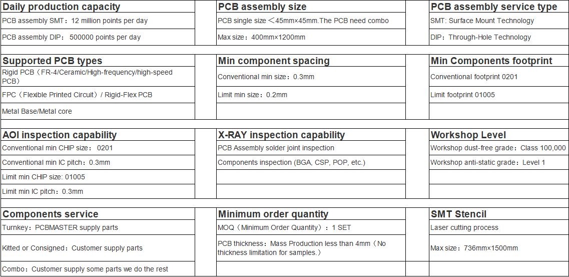
PCBMASTER: PCB assembly capability
PCBMASTER's FPC Product Introduction :https://www.pcbmaster.com/product?type=4
PCBMASTER's FPC Assembly Capabilities:
Contact us anytime to learn more:https://www.pcbmaster.com/login

