







BGA Routing and Via Design Rules: Best Practices for High-Density PCB Layouts
As electronic products continue to integrate more functions into smaller form factors, BGA (Ball Grid Array) packages have become the preferred solution for high-pin-count devices. However, successful BGA implementation depends heavily on routing strategy, via selection, stack-up planning, and manufacturability considerations. For designers working with HDI , high-speed , automotive, industrial, and communication applications, proper BGA fanout and via design directly impact signal integrity, yield, reliability, and production cost. Leveraging advanced manufacturing capabilities, HDI expertise, and strict quality management systems, PCBMASTER supports complex BGA PCB projects from prototype through volume production.
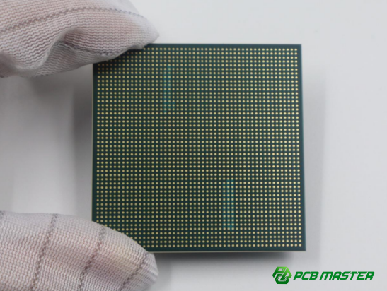
Why BGA Routing Has Become a Critical PCB Design Challenge
Modern ICs continue to evolve toward:
- Higher pin counts
- Smaller package sizes
- Faster signal speeds
- Lower operating voltages
- Greater thermal density
Traditional SMD packages are increasingly replaced by fine-pitch BGAs, often featuring pitches of 0.8 mm, 0.65 mm, 0.5 mm, or even smaller.
While BGAs provide excellent electrical and thermal performance, they also create significant routing challenges:
- Limited escape routing channels
- Reduced spacing between pads
- Increased demand for HDI structures
- Stricter impedance control requirements
- More complex assembly processes
The key objective is to achieve an optimal balance between:
- Signal Integrity (SI)
- Power Integrity (PI)
- Thermal Performance
- Manufacturability (DFM)
- Long-Term Reliability
Core Via Design Rules for BGA Areas
Selecting the Appropriate Via Type
Via selection is one of the most important decisions in BGA design.
| Comparison Item | Recommended Via Type | Typical Application |
| >1.0 mm | Through-Hole Via | Cost-sensitive designs |
| 0.8 mm | Blind Via Preferred | Medium-density routing |
| ≤0.65 mm | Laser Microvia | HDI designs |
| ≤0.5 mm | Via-in-Pad Microvia | Ultra-high-density designs |
Microvias are generally the preferred solution for high-density BGA layouts.
For fine-pitch BGAs, laser-drilled blind and buried vias enable routing that is simply impossible using conventional through-hole vias.
Via-in-Pad Technology
For extremely dense BGAs, via-in-pad technology becomes the most effective routing solution.
Requirements include:
- Resin-filled vias
- Copper plating over the filled via
- Planarized surface finish
- Full cap plating
Benefits:
- Maximum routing density
- Improved thermal conduction
- Reduced signal path length
- Better high-frequency performance
Failure to properly fill and cap the via can result in:
- Solder voids
- Flux entrapment
- Poor solder joint reliability
Via Dimensions
Whenever possible, designers should use the smallest manufacturable via dimensions while maintaining current-carrying capability.
Typical recommendations:
| Via Type | Drill Size | Pad Diameter |
| Laser Blind Via | ~4 mil | ~10 mil |
| Mechanical Via | ≥8 mil (0.20 mm) | ≥18–20 mil |
Key principle:
Always align via dimensions with the PCB manufacturer's qualified process capabilities.
Annular Ring and Anti-Pad Requirements
Proper annular ring design ensures drilling reliability and copper integrity.
Recommendations:
- Maintain manufacturer-required annular ring width.
- Power and ground layers should include sufficient anti-pad clearance.
- Typical isolation ring requirement: ≥0.15 mm (6 mil).
Via Spacing Requirements
Critical spacing parameters include:
- Via-to-via spacing
- Via-to-trace spacing
- Via-to-pad spacing
Designers must satisfy:
- Electrical clearance requirements
- Fabrication tolerances
- Assembly process limitations
Via Filling and Covering
Via-in-Pad Structures
Must include:
- Resin filling
- Copper plating
- Surface planarization
- Copper capping
Non-Via-in-Pad Structures
Generally do not require filling, although plugged vias may be recommended to:
- Prevent solder wicking
- Improve assembly reliability
- Support wave soldering processes
BGA Fanout Design Best Practices
Fanout routing determines whether signals can successfully escape the BGA array.
Recommended Fanout Strategy
The preferred method is the dog-bone fanout :
Pad → Short Trace → Via Pad
Advantages:
- Better manufacturing reliability
- Improved solder joint stability
- Easier assembly inspection
Fanout Guidelines
- Keep escape traces short and direct.
- Maintain consistent routing direction.
- Avoid unnecessary bends.
- Position vias within routing channels whenever possible.
- Use via-in-pad for inner BGA rows when routing density becomes excessive.
Common Fanout Comparison
| Dimension | Conventional Practice | Advanced HDI Practice |
| Escape Density | Limited | High |
| Signal Path Length | Longer | Shorter |
| Routing Layers Required | More | Fewer |
| Fine-Pitch Support | Restricted | Excellent |
| Manufacturing Complexity | Lower | Higher |
Routing Design Rules for Fine-Pitch BGA Packages
Trace Width and Spacing
To maximize routing channels:
- Use the narrowest manufacturable traces.
- Maintain controlled impedance requirements.
- Ensure adequate current-carrying capacity.
Common HDI routing capabilities:
| Design Rule | Typical Value |
| Trace Width | 3–4 mil |
| Trace Spacing | 3–4 mil |
| Advanced HDI | 3/3 mil |
Routing Between BGA Pads
A practical DFM recommendation is:
- Trace width ≥4 mil whenever possible
- Conductor spacing ≥3.5 mil whenever possible
Although more aggressive geometries can sometimes be manufactured, designing at the absolute process limit often reduces yield and narrows supplier options.
Stack-Up Planning
Effective BGA routing begins with proper layer stack-up design.
Key considerations:
- Sufficient signal layers
- Continuous reference planes
- Controlled impedance structures
- Appropriate dielectric thickness
- Power distribution efficiency
For high-speed applications, stack-up planning should occur before component placement.
DFM Considerations That Improve Yield
Teardrops
Adding teardrops between traces and pads:
- Improves mechanical robustness
- Reduces drill breakout risk
- Enhances manufacturing yield
Solder Mask Design
Recommendations:
- Maintain reliable solder mask dams.
- Prevent solder bridging between pads.
- Oversize solder mask openings by approximately 0.05–0.10 mm.
Silkscreen Control
Ensure:
- No silkscreen overlaps pads.
- Clear Pin-1 indicators.
- Readable assembly markings.
Test Point Planning
Adequate test access remains essential for:
- ICT testing
- Functional testing
- Production diagnostics
Industry Best Practices from PCBMASTER
As PCB complexity continues to increase, successful BGA implementation depends heavily on selecting a manufacturing partner with advanced HDI and assembly capabilities.
PCBMASTER provides complete PCB and PCBA services through its 80,000㎡ manufacturing facility, supporting:
- HDI PCB production
- Blind and buried via technology
- Rigid-Flex PCB manufacturing
- High-frequency PCB fabrication
- SMT assembly services
- Engineering design support
Key Advantages
- IATF 16949 certified quality management
- ISO 9001 certified manufacturing systems
- UL certified products
- RoHS compliance
- Free engineering document review
- 24-hour prototype capability
- 99.59% on-time delivery rate
- 99.5% product yield rate
- 24/7 engineering support
For projects involving fine-pitch BGA devices, the engineering team at PCBMASTER assists customers with DFM optimization, stack-up recommendations, manufacturability reviews, and HDI process selection before production begins.
Common Design Mistakes to Avoid
Mistake 1: Designing Beyond Manufacturing Capability
Many PCB failures originate from designs that exceed practical fabrication limits.
Always confirm:
- Minimum trace width/spacing
- Minimum drill size
- Annular ring requirements
- Registration accuracy
before layout completion.
Mistake 2: Using Through-Hole Vias for Ultra-Fine-Pitch BGAs
Fine-pitch BGAs often require microvia technology.
Attempting to use conventional vias can dramatically reduce routing efficiency and increase layer count.
Mistake 3: Ignoring Assembly Requirements
A design that is electrically functional but difficult to assemble may result in:
- Lower yields
- Increased costs
- Production delays
Early collaboration between designers, PCB fabricators, and assemblers is essential.
Conclusion and Future Trends
BGA routing and via design represent one of the most demanding aspects of modern PCB development. As electronic products continue moving toward higher density and higher performance, advanced HDI technologies such as microvias, buried vias, and via-in-pad structures are becoming standard design practices rather than specialized options.
The most successful BGA projects follow four fundamental principles:
- Select the appropriate via technology based on BGA pitch.
- Optimize trace width, spacing, and routing channels within proven manufacturing capabilities.
- Develop a robust stack-up and fanout strategy early in the design process.
- Prioritize DFM and collaborate closely with manufacturing partners.
With certified quality systems, advanced HDI capabilities, rapid prototyping services, and extensive PCB/PCBA expertise, PCBMASTER serves as a practical industry benchmark for supporting complex BGA-based electronic designs from concept to mass production.
Tags: #PCBDesign #BGARouting #HDIPCB #ViaInPad #PCBA #SMT #PCBManufacturing #PCBMASTER #ElectronicsEngineering#DFM #SignalIntegrity
About the Author

Carol Luo
PCB Design EngineerI'm Carol, a PCB Engineer at PCBMASTER with experience in PCB design and manufacturing engineering since 2018. I focus on translating engineering requirements into reliable PCB solutions, with expertise in stack-up design, material selection, and design-for-manufacturing (DFM). I share practical engineering insights from real-world PCB design and production experience.
Visit Carol Luo's Profile