


PCB Panelization Design Guide: Rules, Methods, and SMT Best Practices
A well-designed PCB can still encounter production challenges if the panelization strategy is overlooked. While circuit functionality is determined at the board level, manufacturing efficiency, assembly stability, and overall production cost are often shaped by how individual boards are combined into a panel.
From material utilization and SMT compatibility to depaneling reliability and warpage control, panelization directly affects every stage of the manufacturing process. Even small design decisions can influence yield rates, processing speed, and the risk of component damage during assembly and separation.
Therefore, effective PCB panelization is not simply a manufacturing preference—it is a critical design consideration that bridges engineering requirements and mass-production realities. By understanding the key principles, connection methods, structural requirements, and SMT-related considerations, designers can create panel layouts that support both cost-effective production and long-term product reliability.
What Is PCB Panelization (Panelization)? Why Does Panel Design Affect Yield and Cost?
PCB panelization is the process of combining multiple individual PCBs into a larger manufacturing panel, and its design directly affects production yield and cost by influencing manufacturing efficiency, material utilization, assembly stability, and product reliability.
PCB Panelization Definition and Core Functions
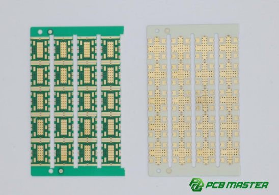
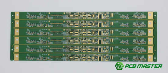
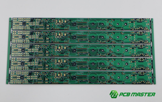
PCB panelization is the process of combining multiple individual printed circuit boards (PCBs) into a larger manufacturing panel. Instead of producing and assembling each board separately, manufacturers process multiple boards together and separate them after assembly. This approach improves production efficiency, reduces handling time, and lowers manufacturing costs.
Difference Between a Single PCB and a PCB Panel
| Item | Single PCB | PCB Panel |
| Definition | One individual circuit board | Multiple PCBs connected into one larger board |
| Manufacturing | Processed individually | Processed as a group |
| SMT Assembly | Lower efficiency | Higher efficiency |
| Material Utilization | Often lower | Usually higher |
| Production Cost | Higher per board | Lower per board |
| Depaneling Required | No | Yes |
| Best For | Prototypes and small batches | Mass production |
Why Are PCB Panels Needed for PCB Manufacturing and SMT Assembly?
PCB fabrication and SMT assembly equipment are designed to handle boards within certain size ranges. Very small PCBs can be difficult for conveyor systems, pick-and-place machines, and inspection equipment to process accurately.
By combining several small boards into a larger panel, manufacturers can:
- Improve machine handling stability
- Increase SMT placement speed
- Reduce manual loading and unloading
- Improve automated inspection efficiency
- Simplify mass production workflows
For example, a 30 mm × 40 mm PCB may be too small for efficient SMT processing. Combining 20 boards into a panel creates a stable manufacturing format that can move smoothly through the production line.
What Is the Value of PCB Panelization in Mass Production?
In high-volume manufacturing, panelization helps optimize the entire production process.
Key benefits include:
- Faster SMT assembly cycles
- Lower labor costs
- Reduced machine setup frequency
- Better material utilization
- More consistent production quality
For example, assembling 100 individual boards one by one requires significantly more handling than assembling five panels containing 20 boards each. This directly improves throughput and reduces manufacturing costs.
Three Key Metrics Influenced by PCB Panel Design
PCB panel design directly affects production efficiency, manufacturing cost, and product reliability. These three factors are often considered the primary goals of successful PCB panelization.
Production Efficiency
A well-designed PCB panel allows SMT equipment to run continuously with fewer interruptions.
Benefits include:
- Faster component placement
- Reduced machine idle time
- Easier loading and unloading
- Improved inspection speed
For example, when all boards are arranged in the same orientation, pick-and-place machines can follow a more efficient placement path, reducing assembly time.
Manufacturing Cost
PCB panelization has a direct impact on both fabrication and assembly costs.
Cost-saving factors include:
- Higher material utilization
- Reduced setup time
- Lower labor requirements
- Faster depaneling operations
A panel utilization rate above 80% is often considered a good target because it minimizes wasted PCB material and reduces overall production expenses.
Product Reliability
Panel design also affects the mechanical and thermal stability of the PCB during production.
Reliable panel designs help:
- Prevent board warpage
- Reduce soldering defects
- Minimize depaneling stress
- Protect sensitive components
For example, balanced panel layouts distribute heat more evenly during reflow soldering, reducing the risk of board deformation.
What Problems Can Poor PCB Panel Design Cause?
Poor panelization can create manufacturing issues that affect yield, quality, and production costs.
SMT Placement Misalignment
If the panel lacks proper structural support or fiducial markings, SMT machines may not position components accurately.
Common results include:
- Component shifting
- Incorrect placement
- Increased rework rates
- Lower assembly yield
Example:
A flexible or unstable panel may slightly bend during transport, causing placement coordinates to shift and reducing assembly accuracy.
Reflow Soldering Warpage and Deformation
Uneven panel structures or unbalanced copper distribution can cause thermal stress during reflow soldering.
Typical problems include:
- PCB warpage
- Lifted corners
- Solder joint defects
- BGA reliability issues
Example:
A panel with heavy copper concentration on one side may expand unevenly during heating, causing the board to warp.
Component Damage During Depaneling
Poorly designed breakaway tabs or V-cut locations can transfer excessive mechanical stress to nearby components.
High-risk components include:
- MLCC capacitors
- BGAs
- Crystal oscillators
- Connectors
Example:
An MLCC capacitor placed too close to a depaneling tab may develop internal cracks when the boards are separated.
Low Material Utilization Increases Manufacturing Cost
Inefficient board arrangement can leave large unused areas on the manufacturing panel.
Consequences include:
- Increased PCB material waste
- Higher fabrication cost per board
- Reduced profitability in volume production
Example:
If only 60% of the available panel area is used, the remaining 40% becomes wasted material, significantly increasing the cost of each finished PCB.
Key Takeaway
PCB panelization is much more than arranging multiple boards on a larger sheet. It is a critical manufacturing design process that directly affects SMT efficiency, production cost, and product reliability. A well-optimized PCB panel can improve material utilization, reduce assembly risks, and support stable, high-yield mass production. Conversely, poor panel design can lead to placement errors, board warpage, component damage, and unnecessary manufacturing expenses.
What Key Factors Should Be Considered When Designing PCB Panel Size?
PCB panel size should match SMT equipment capabilities, maximize material utilization, and maintain enough mechanical strength for stable manufacturing and assembly.
A well-designed PCB panel size helps improve production efficiency, reduce manufacturing costs, and prevent quality problems such as warpage, placement errors, and handling difficulties. The goal is to create a panel that works smoothly throughout PCB fabrication, SMT assembly, inspection, and depaneling.
PCB Panel Size Requirements That Match SMT Equipment Capabilities
Pick-and-Place Machine Maximum Panel Size Limits
Every SMT pick-and-place machine has a minimum and maximum board size it can handle. If a PCB panel is too large, it may exceed machine capacity. If it is too small, the conveyor system may not transport it reliably.
Before finalizing a PCB panel layout, confirm:
- Maximum board size supported by the SMT line
- Minimum board size required for stable transport
- Required panel thickness and rigidity
For example, if a pick-and-place machine supports panels up to 460 mm × 400 mm, designing a larger panel could create production issues or require manual handling.
Reflow Oven Conveyor Width Requirements
The PCB panel must also fit within the width range of the reflow soldering oven. Panels that are too wide may not pass through the conveyor, while panels that are too narrow may lack support during heating.
Key considerations include:
- Conveyor rail width limits
- Panel weight distribution
- Thermal stability during reflow
A properly sized panel reduces the risk of sagging and warpage when exposed to high temperatures.
AOI Inspection Equipment Compatibility
Automated Optical Inspection (AOI) systems inspect solder joints and component placement after assembly. Oversized or unusually shaped panels can affect inspection accuracy.
To improve AOI compatibility:
- Maintain consistent panel dimensions
- Include sufficient fiducial marks
- Avoid excessively large panel formats
For example, a standard rectangular panel is usually easier for AOI systems to scan than an irregularly shaped panel with varying widths.
How Can Higher PCB Panel Utilization Reduce Manufacturing Costs?
Higher panel utilization means more boards are produced from the same material, reducing waste and lowering manufacturing costs.
Recommended PCB Material Utilization Targets
PCB material utilization refers to the percentage of the panel area occupied by usable boards.
General recommendations:
| Utilization Rate | Evaluation |
| Below 70% | Poor |
| 70%–80% | Acceptable |
| Above 80% | Recommended |
| Above 90% | Excellent |
Most PCB manufacturers aim for at least 80% panel utilization to achieve a good balance between cost and manufacturability.
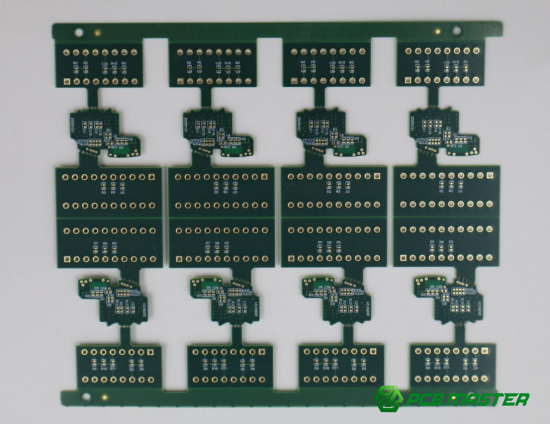
Same-Direction and Interlocking Arrangement Strategies
Board arrangement has a major impact on panel efficiency.
Same-direction arrangement places all boards in the same orientation. This simplifies SMT programming and improves assembly consistency.
Interlocking arrangement rotates or nests boards together to reduce unused space. This is especially useful for irregular PCB shapes.
Example:
A rectangular board may achieve 82% utilization with standard placement, while an interlocking layout can increase utilization to 90% or higher.
Methods for Reducing Edge Waste
Unused space around panel edges directly increases material costs.
Common optimization methods include:
- Reducing excessive panel margins
- Using interlocking board layouts
- Optimizing breakaway tab locations
- Combining different board shapes efficiently
For example, redesigning the board arrangement may allow two additional PCBs to fit on the same panel, reducing cost per unit without changing the product itself.
PCB Panel Size Recommendations for Different Product Types
Small PCB Panelization Solutions
Small PCBs are often difficult for SMT equipment to handle individually. Panelization creates a larger, more stable assembly format.
Recommended approach:
- Combine multiple boards into a larger panel
- Add sufficient process rails
- Maintain good structural rigidity
Example:
A 25 mm × 30 mm PCB may be panelized into a 5 × 6 array to improve assembly efficiency and reduce handling problems.
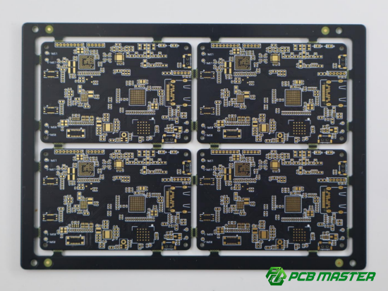
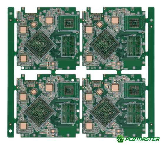
Medium-Size PCB Panelization Solutions
Medium-sized PCBs typically provide the most flexibility for panel design.
Recommended approach:
- Balance panel size and mechanical strength
- Optimize material utilization
- Ensure compatibility with SMT and AOI equipment
A panel containing 4 to 12 boards is common for medium-sized consumer electronics products.
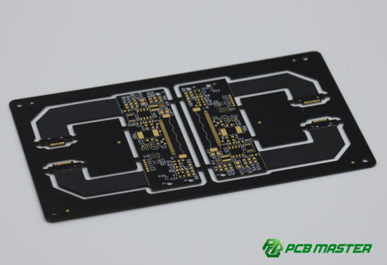
Irregular-Shaped PCB Panelization Solutions
Irregular PCBs often require special panelization methods because they cannot be efficiently arranged in standard grids.
Recommended approach:
- Use breakaway tabs (mouse bites)
- Apply interlocking layouts
- Evaluate stress distribution carefully
Examples include wearable devices, automotive sensors, and uniquely shaped IoT products.
Comparison Tbale
| PCB Type | Characteristics | Recommended Panelization Method | Typical Example |
| Small PCB | Difficult for SMT equipment to handle individually due to small size | • Combine multiple boards into a larger panel• Add sufficient process rails• Maintain good panel rigidity | A 25 mm × 30 mm PCB arranged in a 5 × 6 panel to improve assembly efficiency and handling stability |
| Medium-Size PCB | Offers good balance between manufacturability and panel utilization | • Balance panel size and mechanical strength• Optimize material utilization• Ensure SMT and AOI compatibility | Consumer electronics PCBs commonly arranged in panels containing 4–12 boards |
| Irregular-Shaped PCB | Cannot be efficiently arranged in standard rectangular arrays | • Use breakaway tabs (mouse bites)• Apply interlocking layouts• Carefully evaluate stress distribution during assembly and depaneling | Wearable devices, automotive sensors, and uniquely shaped IoT products |
Common PCB Panel Size Design Mistakes
Oversized Panels Causing Warpage
Large panels may appear cost-effective because they hold more boards, but excessive size can reduce rigidity.
Potential problems include:
- Reflow warpage
- Conveyor instability
- AOI inspection difficulties
For example, a very large panel may bend under its own weight during reflow soldering, creating assembly defects.
Panels That Are Too Small Reduce Production Efficiency
Small panels require more frequent loading, unloading, and machine setup.
Potential problems include:
- Increased labor costs
- Reduced SMT throughput
- Longer production cycles
For example, processing ten small panels instead of two larger optimized panels increases machine handling time significantly.
Poor Utilization of Panel Edge Areas
Many designs leave excessive unused space near panel edges.
Potential problems include:
- Higher material waste
- Increased cost per PCB
- Lower manufacturing efficiency
A common example is leaving large blank areas around process rails when a more compact board arrangement could achieve significantly better utilization.
Key Takeaway
Successful PCB panel size design balances three objectives: equipment compatibility, material utilization, and structural stability. The panel must fit SMT, reflow, and AOI equipment while maximizing usable board area and maintaining enough strength to prevent deformation. By selecting the right panel size and layout strategy, manufacturers can improve production efficiency, reduce PCB fabrication costs, and achieve more consistent assembly quality.
How to Ensure PCB Panel Structural Stability and Transport Strength?
PCB panel stability is ensured by designing enough mechanical support so the panel can withstand SMT handling, high-temperature reflow stress, and depaneling force without bending, cracking, or damaging components.
A stable PCB panel is essential for smooth mass production. If the panel is weak or uneven, it can deform during transport, cause SMT misalignment, or even break during depaneling.
Why Is PCB Panel Structural Stability Important?
Structural stability ensures the PCB panel can survive SMT transport, reflow heating, and depaneling without mechanical damage or production defects.
SMT Transport Force Analysis
During SMT production, PCB panels move through conveyors, pick-and-place machines, and inspection systems. These systems apply continuous mechanical pressure and vibration.
If the PCB panel is not rigid enough:
- The panel may bend during transport
- Component placement accuracy may drop
- Conveyor rails may cause stress points
Example: A thin PCB panel may slightly flex on the conveyor belt, causing misalignment during high-speed component placement.
Reflow Soldering Thermal Stress Impact
During reflow soldering, the PCB is exposed to high temperatures (typically 230°C–260°C). Different materials expand at different rates, creating internal stress.
If the panel design is weak:
- Uneven expansion causes warpage
- Solder joints may crack or lift
- BGA components may become unreliable
Example: A panel with uneven copper distribution may bend upward during heating, leading to solder defects after cooling.
Depaneling Mechanical Stress Impact
After assembly, individual boards must be separated from the panel. This process introduces strong mechanical force, especially in V-cut or mouse-bite designs.
If the structure is not well designed:
- PCB edges may crack
- Nearby components may be damaged
- Internal traces may break
Example: A fragile MLCC capacitor placed too close to a break line may crack when the panel is snapped apart.
What Are the Main Factors Affecting PCB Panel Strength?
PCB panel strength depends on material thickness, base material type, connection structure design, and overall panel size ratio.
PCB Thickness
Thicker PCBs are generally stronger and more resistant to bending during SMT and reflow.
- 1.6 mm PCB: standard stability for most products
- 1.0 mm or thinner: higher risk of warpage
- 2.0 mm: very stable but higher cost
Example: Thin IoT boards often require extra support rails due to low rigidity.
Material Type
Different PCB materials affect thermal and mechanical strength
- FR-4: standard balance of cost and strength
- High-Tg FR-4: better heat resistance and stability
- Flexible PCB: very low rigidity, requires special panel support
Example: Automotive electronics often use high-Tg materials to resist high-temperature deformation.
Connection Tab Design
Connection structures (V-cut or mouse bites) determine how stress is distributed across the panel.
Key design points:
- More connection points = stronger panel
- Poorly placed tabs = stress concentration
- Uneven distribution = warpage risk
Example: A panel with only two support tabs on one side may bend during reflow.
Panel Size Ratio
Large panels with thin structures are more likely to deform.
- Large size + thin PCB = high warpage risk
- Balanced aspect ratio = better stability
- Compact layout = improved rigidity
Example: A long, narrow panel behaves like a ruler and bends easily under heat.
How to Prevent PCB Panel Deformation in Design?
Deformation is prevented by adding support points, improving structure layout, and balancing mechanical forces across the entire panel.
Increasing Number of Connection Points
More support points distribute mechanical stress evenly.
Best practices:
- Add multiple break tabs on long edges
- Avoid single-point support areas
- Ensure symmetrical placement
Example: A 4-side supported panel is much more stable than a 2-side supported panel.
Optimizing Support Structure Layout
Good structural layout improves stiffness without increasing material cost.
Methods include:
- Adding internal support rails
- Using cross-shaped reinforcement patterns
- Avoiding large empty spaces
Example: Adding a central support strip can reduce bending during reflow heating.
Balancing Overall Force Distribution
Even force distribution prevents localized stress concentration.
Design strategies:
- Symmetrical component layout
- Balanced copper distribution
- Even weight distribution across the panel
Example: Placing heavy components only on one side often leads to uneven warpage after reflow.
How to Balance Structural Strength and Easy Depaneling?
The key is to design a panel that is strong enough for manufacturing but weak enough to be safely separated without damaging components.
Problems of Excessive Strength
If the PCB panel is too strong:
- Depaneling becomes difficult
- Excess force is needed to break boards
- Risk of damaging components increases
Example: Over-reinforced mouse-bite tabs may require excessive force, cracking nearby MLCC capacitors.
Problems of Insufficient Strength
If the PCB panel is too weak:
- Panels may break during SMT transport
- Warpage increases during reflow
- Yield rate decreases
Example: Weak V-cut design may cause accidental separation during conveyor movement.
Recommended Design Principles
To balance strength and depaneling efficiency:
- Use moderate number of connection tabs
- Maintain symmetrical support layout
- Avoid placing sensitive components near break lines (≥5 mm recommended)
- Validate through trial production before mass manufacturing
Example: A well-balanced design allows clean hand or machine depaneling with minimal stress while keeping the panel stable during full SMT processing.
Key Takeaway
PCB panel structural stability is a balance between rigidity for manufacturing and controlled weakness for depaneling. A successful design ensures smooth SMT transport, stable performance during reflow soldering, and safe separation without damaging components or reducing yield.
What Are the Key Design Requirements for V-Cut PCB Panelization?
V-Cut panel design requires precise groove depth control, correct structural layout, and strict component clearance rules to ensure clean separation without damaging the PCB or components.
V-Cut (V-scoring) is one of the most common PCB depaneling methods in PCB panelization design. Proper design ensures smooth separation, high production efficiency, and low risk of edge damage during mass production.
What Is V-Cut Panelization?
V-Cut panelization is a PCB separation method where V-shaped grooves are cut on both sides of the board so the PCB can be easily snapped apart after assembly.
V-Cut Process Principle
V-Cut uses a mechanical cutting blade to create a V-shaped groove on the top and bottom surfaces of the PCB panel. The board is not fully cut through; instead, a thin section of material remains in the middle.
During depaneling:
- The PCB is separated by applying controlled mechanical force
- The remaining thin core breaks along the V-line
- Boards are separated into individual units
Example: In mass production of router PCBs, V-Cut allows fast and clean separation without additional routing tools.
Suitable Product Types for V-Cut
V-Cut is best used for PCB panelization designs that require straight-line separation.
Typical applications include:
- Consumer electronics PCBs
- LED lighting boards
- Power supply modules
- Standard rectangular circuit boards
It is not suitable for highly irregular PCB shapes or boards requiring curved separation paths.
Which PCB Shapes Are Suitable for V-Cut Panelization?
V-Cut is mainly suitable for rectangular PCB designs and regular grid-based panel layouts with straight-line depaneling paths.
Standard Rectangular PCB Boards
Rectangular PCBs are the most ideal structure for V-Cut panelization.
Advantages:
- Simple straight-line cutting paths
- High manufacturing efficiency
- Low depaneling cost
Example: A 50 mm × 80 mm PCB can be arranged in a grid and separated easily using V-Cut lines.
Regular Array Panel Designs
V-Cut is also suitable for multi-board array layouts where all boards are aligned in rows and columns.
Key characteristics:
- Uniform spacing between boards
- Straight V-Cut lines across the panel
- High compatibility with SMT production lines
Example: A 4×6 PCB array used in LED driver manufacturing improves throughput and reduces handling time.
What Are the Key V-Cut Design Parameters?
V-Cut design must control groove depth, remaining board thickness, and cutting precision to ensure safe and clean PCB separation.
V-Groove Depth Design Standard
The V-groove depth determines how easily the PCB can be separated.
Typical rule:
- V-Cut depth = 1/3 to 1/4 of PCB thickness (per side)
Example:
For a 1.6 mm PCB:
- Each side cut depth ≈ 0.4 mm
- Ensures stable cutting and controlled break force
If the groove is too shallow → difficult depanelingIf too deep → risk of accidental breakage
V-Groove Remaining Thickness Requirement
The remaining PCB thickness (core material) is critical for safety during SMT handling.
Recommended range:
- 0.3 mm – 0.6 mm remaining thickness
Function:
- Maintains panel strength during SMT process
- Ensures controlled snapping during depaneling
Example: Thin remaining thickness makes separation easier but increases risk of accidental cracking during transport.
Blade Angle and Cutting Precision Requirements
V-Cut blades must maintain strict angle and alignment control.
Key requirements:
- Standard blade angle: ~30° to 45°
- Alignment deviation must be minimal
- Consistent cutting depth across the entire panel
If precision is poor:
- Uneven break lines
- Increased burr formation
- Higher risk of PCB edge damage
Example: Misaligned V-Cut lines can cause one side to break earlier, damaging nearby components.
What Layout Restrictions Apply to V-Cut Areas?
V-Cut areas must be kept free of components, vias, and copper to avoid mechanical stress damage during depaneling.
Component Clearance Requirements
Components must be kept away from V-Cut lines to avoid mechanical stress during snapping.
Recommended rule:
- Minimum distance: ≥ 5 mm from V-Cut line
High-risk components include:
- MLCC capacitors
- IC packages
- Connectors
Example: A capacitor placed too close to a V-Cut line may crack during depaneling due to bending stress.
Via Clearance Requirements
Vias near V-Cut lines can weaken structural integrity.
Design rule:
- Keep vias away from V-Cut groove area
- Avoid via placement on or near scoring lines
Problem if ignored:
- Internal copper cracking
- Signal discontinuity
- Mechanical weakness
Copper Pour Keep-Out Requirements
Copper should be removed or restricted near V-Cut lines.
Reason:
- Copper stiffness causes uneven stress distribution
- Can lead to PCB fracture during separation
Best practice:
- Add copper keep-out zones along V-Cut lines
- Maintain balanced copper distribution across panel
Example: Uneven copper near cut lines often causes irregular break edges.
What Are the Common Failure Issues in V-Cut Panel Design?
Common V-Cut failures include rough edges, PCB cracking, and component damage caused by poor groove design or improper layout.
Burrs and Rough Edges After Depaneling
If blade sharpness or depth control is poor:
- PCB edges may become rough
- Fiberglass burrs may appear
- Assembly quality is reduced
Example: Poor V-Cut maintenance results in uneven separation lines that require additional cleaning.
PCB Edge Cracking
Excessively deep or uneven V-Cut grooves can weaken the PCB.
Possible results:
- Random cracking during transport
- Breakage outside intended cut line
- Structural failure in thin boards
Example: A deeply scored PCB may snap prematurely during SMT conveyor movement.
Component Stress Damage
Improper layout near V-Cut lines leads to mechanical stress transfer.
Common issues:
- Cracked MLCC capacitors
- Damaged solder joints
- IC package stress failure
Example: A tightly placed IC near a V-Cut line may experience micro-cracks after repeated handling and depaneling.
Key Takeaway
V-Cut PCB panelization requires precise control of groove depth, structural balance, and component clearance. When designed correctly, it enables fast, low-cost, and high-yield PCB separation. When poorly designed, it can lead to edge damage, component failure, and reduced manufacturing reliability in mass production.
How Do Mouse Bite (Stamp Hole) PCB Panel Designs Balance Strength and Depaneling Efficiency?
Mouse bite PCB panelization balances mechanical strength and easy separation by using perforated holes (stamp holes) that provide support during SMT while allowing controlled break-off after assembly.
Mouse bite (also called break-off tabs or stamp holes PCB panelization) is widely used for irregular PCB shapes where V-Cut cannot be applied. It provides a flexible and reliable depaneling method for complex designs.
What Is Mouse Bite (Break-off Tabs) PCB Panelization?
Mouse bite PCB panelization connects individual boards using small drilled holes arranged in a row, allowing boards to be snapped apart after SMT assembly.
Mouse bite design uses a series of small holes along the PCB edge to create a weak mechanical line. During depaneling, the board is manually or mechanically separated along this perforated line.
Key characteristics:
- No V-groove cutting required
- Suitable for curved or irregular edges
- Provides moderate mechanical strength during SMT
Example: Wearable device PCBs often use mouse bite tabs because their rounded shapes cannot be cut using straight V-Cut lines.
Which PCB Products Are Suitable for Mouse Bite Panelization?
Mouse bite panelization is ideal for irregular, curved, or non-rectangular PCB designs that cannot use straight-line V-Cut separation.
Irregular-Shaped PCBs
Irregular PCB designs often include missing corners, cutouts, or uneven edges.
Why mouse bite is used:
- V-Cut cannot follow non-straight edges
- Flexible panel layout is required
- Easier adaptation to product housing
Example: Smart home sensors with uneven PCB outlines often rely on mouse bite tabs for panelization.
Curved PCB Shapes
Curved PCB edges are common in modern compact electronic products.
Why mouse bite is suitable:
- Supports non-linear separation lines
- Avoids mechanical routing complexity
- Maintains assembly stability
Example: Fitness tracker PCBs often have curved edges to fit wristband housings.
Polygon-Shaped PCB Designs
Polygon PCBs (e.g., hexagonal or trapezoidal shapes) require flexible connection structures.
Benefits:
- Allows efficient panel packing
- Reduces wasted PCB material
- Supports custom product geometries
Example: LED decorative modules often use polygon-shaped PCBs to fit complex lighting layouts.
What Are the Key Design Parameters for Mouse Bite PCB?
Key parameters include hole size, hole spacing, connection strength width, and routing clearance, all of which determine strength and break quality.
Hole Diameter Design Standard
Hole size directly affects breaking force and edge quality.
Typical range:
- 0.4 mm – 0.6 mm drill diameter
Guidelines:
- Smaller holes → cleaner break but weaker support
- Larger holes → stronger support but harder to separate
Example: Consumer electronics often use 0.5 mm holes for balanced performance.
Hole Spacing Design Standard
Hole spacing determines how easily the board separates.
Recommended range:
- 0.25 mm – 0.35 mm between holes
Design impact:
- Tight spacing → easier depaneling, weaker strength
- Wider spacing → stronger panel, harder separation
Example: High-density IoT boards use tighter spacing to improve depaneling efficiency.
Connection Web Width Design Standard
The connection web is the remaining material between drilled holes.
Recommended value:
- Around 0.5 mm – 1.0 mm
Function:
- Provides mechanical strength during SMT
- Controls break force during depaneling
Example: Too thin → accidental break during transport; too thick → high separation force required.
Routing (Milling) Clearance Design Standard
The routing gap defines the separation path between boards.
Key points:
- Typically 1.5 mm – 2.5 mm width
- Ensures milling tool can pass cleanly
- Prevents copper damage during depaneling
Example: Insufficient clearance may cause rough edges or incomplete separation.
How Should Connection Points Be Planned in Mouse Bite PCB Design?
Connection points must be distributed evenly and symmetrically to balance mechanical stress and prevent uneven breakage.
Load-Balancing Principle
Stress must be evenly distributed across all connection tabs.
Design rules:
- Avoid clustering tabs in one area
- Ensure uniform spacing along edges
- Reinforce high-stress zones
Example: A panel with uneven tabs may crack on one side first during depaneling.
Symmetrical Distribution Principle
Symmetry improves stability during SMT and reflow.
Best practices:
- Mirror connection points on opposite sides
- Maintain balanced structure layout
- Avoid single-sided support
Example: Symmetrical designs reduce warpage during high-temperature reflow processes.
Long Edge vs Short Edge Layout Strategy
Different edge lengths require different support strategies.
Guidelines:
- Long edges → more connection points needed
- Short edges → fewer points required
- Corner areas → reinforced support recommended
Example: A rectangular panel may require twice as many tabs on long edges to maintain rigidity.
Mouse Bite vs V-Cut PCB Panelization Comparison
Mouse bite offers higher design flexibility, while V-Cut provides higher efficiency and cleaner separation for standard rectangular PCBs.
| Comparison Item | Mouse Bite (Break-off Tabs) | V-Cut (V-Scoring) |
| Suitable PCB Shape | Irregular / curved boards | Standard rectangular boards |
| Depaneling Efficiency | Medium | High |
| Edge Quality | Slightly rough | Clean and smooth |
| Design Flexibility | High | Low |
| Mechanical Strength | Moderate | High |
| Cost Efficiency | Medium | High for mass production |
Example:
- Mouse bite is preferred for wearable and IoT devices
- V-Cut is preferred for consumer electronics like routers and LED drivers
Key Takeaway
Mouse bite PCB panelization is a flexible depaneling solution designed for irregular PCB shapes, but it requires careful control of hole size, spacing, structural balance, and connection strength. When properly designed, it achieves a good balance between manufacturing stability during SMT and controlled separation after assembly, making it essential for modern compact electronic products with complex geometries.
What Are the SMT Manufacturing Requirements for PCB Panel Design?
SMT production requires PCB panels to have proper process edges, accurate fiducial marks, consistent orientation, and optimized layouts to ensure stable, fast, and accurate automated assembly.
SMT (Surface Mount Technology) lines are highly automated systems. PCB panel design must match machine handling, optical recognition, and conveyor transport requirements to avoid production errors and improve yield.
What Are the Process Edge Design Standards and Key Considerations?
Process edges (also called tooling rails) must provide enough mechanical support for SMT machines to grip, transport, and align PCB panels safely.
Process Edge Width Requirements
Process edges are the extra PCB material around the panel used for machine handling.
Standard requirement:
- Minimum width: ≥ 5 mm (typical SMT production line)
- Double-side rails preferred for large panels
Function:
- Provide grip area for conveyors
- Prevent component damage during edge contact
- Improve mechanical stability during SMT
Example: A panel without sufficient process edge may slip or misalign during pick-and-place operation.
Single-Side vs Double-Side Process Edge Selection
The number of process edges depends on panel size and production equipment.
Options:
- Single-side edge: used for compact or cost-sensitive designs
- Double-side edge: preferred for high-speed SMT lines
ComparisonTable:
| Process Edge Type | Description | Advantages | Disadvantages | Typical Use Case |
| Single-side process edge | Only one side of the PCB panel has a tooling rail for SMT handling |
|
|
Compact PCB designs or cost-sensitive products with lower SMT precision requirements |
| Double-side process edge | Tooling rails are added on both sides of the PCB panel |
|
|
High-volume SMT production lines such as consumer electronics, smartphones, and precision PCB assemblies |
Example: High-volume smartphone PCB production typically uses double-side rails for precision handling.
Keep-Out Area (No-Copper Zone) Requirements
The process edge must remain free of copper, vias, and components.
Rules:
- No components or vias within 3 mm–5 mm of edge
- No copper traces in tooling rail area
- Keep-out zones must be clearly defined in PCB design files
Purpose:
- Prevent damage from conveyor clamps
- Avoid electrical short risk
- Improve board strength during transport
Example: A via placed too close to the edge may crack under mechanical stress from SMT fixtures.
How Should Fiducial Marks Be Designed in PCB Panelization?
Fiducial marks must be clearly visible, correctly sized, and properly isolated to ensure accurate optical alignment during SMT placement.
Number of Fiducial Marks per Panel
Fiducials help machines locate the PCB position accurately.
Standard guideline:
- At least 3–4 global fiducials per panel
- Additional local fiducials for high-precision components
Purpose:
- Improve placement accuracy
- Reduce alignment errors
- Support automated optical calibration
Example: BGA-heavy boards often require extra local fiducials for precise chip alignment.
Fiducial Size Specifications
Fiducials must be large enough for optical recognition but not too large to interfere with routing.
Standard size:
- Diameter: 1.0 mm (typical copper pad)
- Solder mask opening: 2.0–3.0 mm
Key rule:
- Must be clearly visible and high contrast
Example: Too small fiducials may not be detected by SMT vision systems, causing placement offset.
Solder Mask Opening Requirements
Fiducials must have clear solder mask openings to ensure optical detection.
Design rules:
- No solder mask covering the pad
- Clean circular opening preferred
- Avoid irregular shapes
Purpose:
- Improve machine vision recognition
- Reduce false detection errors
Example: Poor mask alignment can confuse AOI systems and reduce placement accuracy.
Isolation Area Design Requirements
Fiducials must be isolated from copper and other markings.
Recommended clearance:
- ≥ 3 mm clear zone around fiducial
Avoid:
- Nearby silkscreen text
- Copper pours
- Via clusters
Example: A cluttered fiducial area can reduce recognition accuracy during high-speed SMT scanning.
How Does PCB Panel Orientation Affect SMT Assembly Efficiency?
Panel orientation directly affects machine movement efficiency, placement speed, and production stability.
Same-Direction Panel Layout
All PCBs are oriented in the same direction.
Advantages:
- Simplifies SMT programming
- Faster pick-and-place movement
- Lower risk of placement errors
Example: Consumer electronics panels often use same-direction layout for high-speed mass production.
180° Rotated Alternating Layout
Boards are rotated 180 degrees in alternating rows.
Advantages:
- Improves panel space utilization
- Reduces material waste
- Maintains acceptable SMT efficiency
Example: Small IoT devices often use alternating layouts to maximize PCB usage.
Why Random Orientation Layouts Are Not Recommended
Random orientation causes serious production issues.
Problems include:
- Increased SMT programming complexity
- Slower machine movement paths
- Higher risk of placement errors
- AOI inspection confusion
Example: Mixed-orientation panels often require manual correction, increasing production cost and time.
What Are the AOI and SPI Requirements for PCB Panel Design?
AOI (Automated Optical Inspection) and SPI (Solder Paste Inspection) require consistent panel design, clear marking, and optimized layout paths for accurate inspection.
Inspection Path Optimization
Panels must be designed for smooth scanning paths.
Best practices:
- Align components in consistent rows
- Avoid irregular rotation
- Maintain predictable inspection flow
Purpose:
- Reduce machine travel time
- Improve inspection speed
- Increase production throughput
Example: Straight-line panel layouts are easier for AOI scanning than irregular shapes.
Fiducial and Marking Recognition Stability
AOI and SPI systems rely heavily on visual markers.
Requirements:
- Stable fiducial positioning
- High contrast marking
- Clean background without interference
Example: Poor contrast between fiducial and copper background can cause misalignment in SPI solder paste inspection.
Methods to Improve Inspection Efficiency
Design improvements for better AOI/SPI performance:
- Standardize component orientation
- Add sufficient fiducials per panel
- Avoid dense silkscreen near inspection zones
- Keep consistent spacing between boards
Example: A well-structured panel can reduce AOI inspection time by 20–30% in high-volume production.
Key Takeaway
SMT-compatible PCB panel design must ensure mechanical stability, optical alignment accuracy, and consistent layout orientation. By optimizing process edges, fiducials, board orientation, and inspection paths, manufacturers can significantly improve SMT yield, reduce production errors, and increase overall assembly efficiency in mass production environments.
How Can PCB Panel Design Reduce Reflow Warpage Risk?
PCB panel design reduces reflow warpage by balancing heat distribution, material structure, and mechanical stress so the board expands evenly during high-temperature soldering.
Reflow soldering exposes PCB panels to high temperatures (typically 230°C–260°C). If the structure is uneven, different parts expand at different rates, causing bending or twisting (warpage). Good panel design helps keep the board flat and stable.
What Are the Main Causes of PCB Warpage During Reflow?
PCB warpage mainly comes from uneven thermal expansion, unbalanced copper distribution, and concentrated component weight on the board.
Uneven Thermal Expansion (Thermal Mismatch)
Different materials in the PCB expand at different rates when heated.
Key issue:
- FR-4 substrate expands slowly
- Copper expands differently
- Resin and solder mask behave differently
Result:
- Internal stress builds up
- PCB bends during heating and cooling
Example: A large PCB panel may curl upward after reflow due to uneven heating across its surface.
Unbalanced Copper Distribution
Copper is one of the main structural materials in a PCB. If it is not evenly distributed, the board will bend under heat.
Problems include:
- One side has more copper than the other
- Large copper pours concentrated in one area
- Missing copper on opposite side
Example: A PCB with heavy ground copper on the left side may warp toward that direction during reflow.
Concentrated Component Weight
Heavy components placed in one area create uneven mechanical stress.
Risk factors:
- Large connectors on one side
- BGA or shielding cans clustered together
- Asymmetric component layout
Example: A board with all heavy connectors on one edge may sag or twist during heating and cooling cycles.
How Does Symmetrical Layout Design Reduce Warpage?
Symmetrical layout reduces warpage by evenly distributing components, weight, and heat across the PCB panel.
Balanced Component Distribution
Components should be spread evenly across the board.
Design rule:
- Avoid clustering components in one region
- Mirror placement when possible
- Keep layout centered
Example: Splitting ICs evenly across left and right halves reduces bending stress.
Weight Balance Principle
Mechanical load must be evenly distributed.
Best practices:
- Place heavy components symmetrically
- Avoid single-side heavy loading
- Balance connectors and shielding parts
Example: Two identical connectors placed on opposite sides prevent board tilt during reflow.
Thermal Balance Principle
Heat absorption must be consistent across the PCB.
Design strategies:
- Even copper distribution
- Avoid large thermal mass concentration
- Use thermal relief patterns where needed
Example: A board with uniform copper spread heats evenly and stays flatter during reflow.
What Are Copper Balancing Techniques to Prevent Warpage?
Copper balancing techniques reduce warpage by ensuring even copper coverage and consistent thermal expansion across the PCB panel.
Copper Filling in Empty Areas
Empty PCB areas should be filled with copper to balance structure.
Benefits:
- Improves mechanical rigidity
- Reduces uneven expansion
- Stabilizes heat distribution
Example: Adding copper pour in blank regions prevents one side from expanding faster than the other.
Net Copper vs Non-Net Copper Usage
Copper can be connected (net copper) or isolated (dummy copper).
Guidelines:
- Use dummy copper for balance
- Avoid large isolated copper gaps
- Maintain symmetry in copper layout
Example: Adding unconnected copper islands helps balance thermal stress without affecting circuit function.
Copper Area Balancing Control
Total copper area should be evenly distributed.
Design rules:
- Match copper percentage on both sides
- Avoid extreme density differences
- Maintain mirrored copper patterns when possible
Example: A PCB with 70% copper on one side and 30% on the other is highly likely to warp during reflow.
How to Prevent Warpage in High-Layer Count PCB Panel Design?
High-layer PCB warpage is controlled by managing internal stress, improving material balance, and optimizing large panel structure design.
Multilayer PCB Stress Control
Each layer in a multilayer PCB introduces internal stress.
Key control methods:
- Use symmetrical layer stacking (e.g., 4+4 structure)
- Balance copper distribution across layers
- Avoid uneven dielectric thickness
Example: A symmetrical stack-up reduces internal bending forces after lamination and reflow.
Large Panel Optimization Strategies
Large PCB panels are more prone to warpage due to their size and flexibility.
Optimization methods:
- Add reinforcement rails in panel design
- Reduce unsupported large empty areas
- Improve connection tab distribution
Example: Adding a central support strip in a large panel significantly improves flatness during reflow.
Key Takeaway
PCB reflow warpage can be effectively reduced through balanced copper design, symmetrical component layout, and optimized panel reinforcement structures. In mass production, controlling these factors ensures better flatness, higher SMT yield, and more stable long-term product reliability.
What Reliability Risks Should Be Avoided in PCB Depaneling Design?
PCB depaneling design must avoid excessive mechanical stress, which can damage sensitive components, crack solder joints, and reduce long-term product reliability.
Depaneling (board separation) is one of the most mechanically stressful steps in PCB manufacturing. If not properly designed, the force applied during V-Cut or mouse bite separation can directly transfer to nearby components and internal solder joints.
How Does Depaneling Stress Affect Electronic Components?
Depaneling stress creates bending and torsion forces that can crack solder joints, damage component bodies, and weaken internal PCB connections.
During PCB depaneling, force is applied to break the connection between boards. This force creates:
- Local bending near the cut line
- Sudden mechanical shock
- Stress concentration at weak points
Example: If a PCB is snapped too close to a fragile component, the bending force may transfer into the solder joints, causing invisible micro-cracks that later lead to field failures.
Which Components Are Most Vulnerable to Depaneling Damage?
Small ceramic components, sensitive packages, and mechanically rigid parts near break lines are most likely to be damaged during PCB depaneling.
MLCC Capacitors
MLCC (Multilayer Ceramic Capacitors) are extremely brittle.
Risk:
- Internal micro-cracks from bending stress
- Latent failures after thermal cycling
Example: A 0402 capacitor placed near a V-Cut line may crack during depaneling even if it looks fine initially.
BGA Components
BGA (Ball Grid Array) packages are sensitive to board flexing.
Risk:
- Solder ball fatigue
- Hidden joint cracks
- Reduced long-term reliability
Example: A BGA chip near a mouse bite area may fail after repeated thermal expansion cycles due to early solder damage.
Crystal Oscillators
Crystal oscillators are sensitive to mechanical shock.
Risk:
- Frequency drift
- Internal crystal fracture
- Signal instability
Example: A quartz oscillator near a break line may show unstable timing after depaneling stress.
Connectors
Connectors are rigid and often large, making them stress concentrators.
Risk:
- Pad lifting
- Solder joint fracture
- Mechanical misalignment
Example: A USB connector placed too close to a depaneling edge may loosen after snapping the board.
What Is the Recommended Safe Distance from Connection Tabs?
Sensitive components should be kept at least 5 mm away from depaneling lines, with stricter rules for high-risk components like MLCC and BGAs.
Standard Safe Distance Guidelines
General PCB design rule:
- Minimum distance: ≥ 5 mm from V-Cut or mouse bite line
- Better reliability: 6–10 mm for mass production
Purpose:
- Reduces bending stress impact
- Improves mechanical safety margin
- Prevents solder joint cracking
Example: Increasing component distance from 3 mm to 6 mm significantly reduces MLCC cracking rate in high-volume production.
Special Requirements for High-Risk Components
Some components require stricter spacing rules.
High-risk guidelines:
- MLCC capacitors: ≥ 6–10 mm
- BGA packages: ≥ 8–10 mm
- Crystals: ≥ 6 mm minimum
- Large connectors: ≥ 10 mm preferred
Example: Automotive-grade PCB designs often enforce stricter spacing due to vibration and thermal stress requirements.
How Can Mechanical Stress in Depaneling Be Reduced?
Mechanical stress can be reduced by optimizing tab placement, using proper depaneling tools, and designing stress relief structures in the PCB panel.
Optimizing Connection Tab Position
Proper placement of V-Cut or mouse bite tabs reduces uneven force distribution.
Best practices:
- Distribute tabs evenly along edges
- Avoid placing all tabs on one side
- Reinforce corners with balanced support
Example: A symmetrical tab layout prevents one side of the PCB from snapping earlier than the other.
Using Professional Depaneling Equipment
Manual breaking increases risk of uncontrolled stress.
Recommended methods:
- V-Cut machine depaneling (preferred for high volume)
- Controlled milling separation
- Avoid excessive manual snapping
Example: Using a depaneling machine reduces component damage rate compared to manual hand-breaking in mass production.
Adding Stress Relief Design Features
Stress relief structures help absorb mechanical force before it reaches components.
Common methods:
- Adding routing slots near break lines
- Increasing spacing near high-stress zones
- Using gradual transition edges instead of sharp cuts
Example: A routed relief slot can reduce stress transfer to nearby MLCC components during board separation.
Key Takeaway
PCB depaneling reliability depends on proper component placement, safe distance rules, and optimized mechanical structure design. By controlling stress distribution and using professional separation methods, manufacturers can significantly reduce hidden damage, improve yield rate, and ensure long-term product reliability in mass production.
How to Develop a PCB Panelization Design That Meets Mass Production Requirements?
A production-ready PCB panel design must follow a structured workflow that aligns manufacturer capabilities, SMT equipment limits, and real production validation to ensure stable yield, low cost, and high reliability.
In PCB mass production, panel design is not only a design task but also a manufacturing coordination process. A well-designed PCB panel reduces defects, improves SMT efficiency, and ensures smooth scaling from prototype to mass production.
What Are the Step-by-Step PCB Panel Design Processes?
PCB panel design follows a structured process: confirm fabrication capability, match SMT requirements, select connection method, design tooling features, verify strength, and validate through trial production.
Step 1: Confirm PCB Manufacturer Capabilities
The first step is to check what the PCB fabrication factory can actually support.
Key checks:
- Maximum and minimum panel size
- V-Cut and routing precision capability
- Minimum drill size for mouse bite holes
- Material thickness limits
Example: A factory may only support V-Cut for boards up to 450 mm width, which directly affects panel layout planning.
Step 2: Confirm SMT Equipment Requirements
PCB panel must match SMT line constraints.
Key factors:
- Pick-and-place machine board size limits
- Conveyor width compatibility
- Reflow oven rail support
- AOI/SPI inspection format requirements
Example: If SMT equipment supports only standard rectangular panels, irregular layouts must be adjusted before production.
Step 3: Select PCB Panel Connection Method
Choose the correct depaneling method based on PCB shape and strength requirements.
Options:
- V-Cut for rectangular, high-volume boards
- Mouse bite for irregular shapes
- Mixed methods for complex designs
Example: A router PCB uses V-Cut, while a wearable device uses mouse bite tabs due to curved edges.
Step 4: Design Process Edges and Fiducial Marks
Tooling features ensure stable SMT handling and alignment.
Key design elements:
- Add ≥5 mm process edges
- Include 3–4 global fiducial marks
- Ensure clean solder mask openings
- Maintain keep-out zones for copper and vias
Example: Missing fiducials can cause SMT misalignment, leading to placement errors in high-speed production.
Step 5: Verify Structural Strength of PCB Panel
Mechanical stability must be checked before production.
Key checks:
- Panel rigidity during transport
- Stress distribution during reflow
- Strength of connection tabs or V-Cut lines
Example: A weak panel may bend during conveyor movement, causing component misplacement.
Step 6: Trial Production and Optimization
Small-scale production is used to validate real-world performance.
Key goals:
- Verify depaneling quality
- Check SMT yield rate
- Identify warpage or stress issues
- Optimize layout before mass production
Example: A prototype run may reveal MLCC cracking near V-Cut lines, requiring layout adjustment.
What Key Parameters Must Be Confirmed with PCB and SMT Manufacturers?
Manufacturers must confirm V-Cut tooling, mouse bite capability, minimum process edge size, and panel size limits before finalizing PCB panel design.
V-Cut Tooling Specifications
Important parameters:
- Blade angle (typically 30°–45°)
- Maximum cutting depth accuracy
- Minimum remaining PCB thickness
Purpose:
- Ensure clean and controlled separation
- Avoid PCB edge cracking
Example: Incorrect blade angle may lead to uneven break lines and rough edges.
Mouse Bite (Stamp Hole) Capability
Not all factories support fine pitch drilling.
Key checks:
- Minimum drill diameter (e.g., 0.4–0.6 mm)
- Hole spacing capability (0.25–0.35 mm typical)
- Routing precision
Example: If hole spacing is too wide, depaneling force increases and risk of cracking rises.
Minimum Process Edge Requirements
Process edges must match SMT handling requirements.
Standard:
- ≥5 mm width recommended
Function:
- Machine gripping area
- Conveyor stability
lProtection from component damage
Example: Too narrow rails may cause unstable PCB movement during SMT assembly.
PCB Panel Size Limitations
Panel size must fit both fabrication and SMT equipment.
Key limits:
- Maximum panel width and length
- Conveyor compatibility
- Reflow oven width restrictions
Example: Oversized panels may require manual handling, increasing production cost and risk.
What Should Be Checked in First Article PCB Panel Validation?
First article testing must evaluate depaneling quality, warpage, component damage rate, and SMT production efficiency.
Depaneling Yield Rate
This measures how cleanly boards separate after assembly.
Key indicators:
- Clean break lines
- No edge cracking
- No PCB delamination
Example: Low yield may indicate weak V-Cut depth control.
Warpage Condition
PCB flatness after reflow must be checked.
Key checks:
- Board bending level
- Twist or bow deformation
- Stability during cooling
Example: Excessive warpage may require copper balancing or layout redesign.
Component Damage Rate
Sensitive components must be inspected after depaneling.
Key risks:
- MLCC cracking
- BGA stress failure
- Connector loosening
Example: High MLCC failure rate often indicates insufficient distance from V-Cut lines.
SMT Production Efficiency
Efficiency determines whether panel design is practical for mass production.
Key metrics:
- Placement speed
- Machine idle time
- Handling efficiency
Example: Poor panel orientation may slow down pick-and-place programming and reduce throughput.
Key Takeaway
A production-ready PCB panel design requires a complete closed-loop process: capability check, SMT matching, structure design, validation, and optimization. Only by combining manufacturing constraints with real trial production feedback can designers achieve stable mass production with high yield, low cost, and minimal reliability risk.
What Are the Common PCB Panelization Design Mistakes and How Can They Be Avoided?
Common PCB panelization mistakes include poor material utilization, weak mechanical structure, incorrect component placement near break lines, and lack of manufacturing consideration, all of which reduce yield and increase production cost.
PCB panel design mistakes often only become visible during SMT production or depaneling. These issues can lead to board damage, lower efficiency, and unstable mass production performance.
Low PCB Material Utilization
Low utilization happens when too much empty space is left on the panel, increasing PCB material waste and raising production cost per board.
Poor layout planning often results in large unused areas on the panel.
Key problems:
- Wasted PCB substrate material
- Higher cost per unit board
- Lower production efficiency
Example: A panel using only 65% of available area wastes 35% of material, significantly increasing cost in high-volume manufacturing.
How to avoid it:
- Use interlocking PCB layout when possible
- Optimize board rotation (0°/180° arrangement)
- Minimize non-functional spacing between boards
Insufficient Connection Tabs Causing Panel Breakage
Too few connection points reduce panel strength, making it easy for boards to break or deform during SMT transport and reflow.
If the panel is not well supported, mechanical stress can cause premature cracking.
Key problems:
- PCB cracking during handling
- Warpage during reflow
- Panel instability in SMT line
Example: A long PCB panel with only two support tabs may bend or snap during conveyor movement.
How to avoid it:
- Increase number of connection tabs evenly
- Balance support on all edges
- Reinforce long side areas
Placing Components in V-Cut Areas
Placing components near V-Cut lines causes mechanical stress during depaneling, leading to component cracking or solder joint failure.
V-Cut areas experience bending force when boards are separated.
Key risks:
- MLCC capacitor cracking
- BGA solder joint damage
- Connector loosening
Example: A capacitor placed 2 mm from a V-Cut line may develop micro-cracks after depaneling.
How to avoid it:
- Keep components at least 5 mm away from V-Cut lines
- Increase distance for sensitive components
- Avoid routing traces near break lines
Non-Standard Fiducial Design
Poor fiducial design reduces SMT alignment accuracy, leading to placement errors and lower assembly yield.
Fiducials are optical reference points used by SMT machines.
Key problems:
- Misalignment during pick-and-place
- AOI detection errors
- Reduced placement accuracy
Example: Missing or unclear fiducials can cause entire component shifts in high-speed SMT production.
How to avoid it:
- Use 3–4 global fiducials per panel
- Ensure proper size (around 1.0 mm copper pad)
- Keep clear 3 mm isolation zone around marks
Insufficient Process Edge Width
Narrow process edges reduce SMT machine stability, causing handling errors and potential PCB damage.
Process edges are required for machine gripping and transport.
Key problems:
- Conveyor misalignment
- Reduced mechanical stability
- Component edge damage
Example: A panel with only 3 mm tooling rails may slip during SMT conveyor transport.
How to avoid it:
- Maintain at least 5 mm process edge width
- Use double-side rails for large panels
- Keep keep-out zones free of copper and vias
Ignoring Reflow Warpage Risk
Ignoring warpage design leads to PCB bending during high-temperature reflow, causing solder defects and assembly failure.
Reflow heating causes thermal expansion stress.
Key problems:
- PCB bow and twist deformation
- BGA solder joint failure
- Uneven component soldering
Example: A large PCB with unbalanced copper may curve upward after reflow cooling.
How to avoid it:
- Use symmetrical PCB layout
- Balance copper distribution
- Add structural reinforcement in panel design
Ignoring Depaneling Stress Analysis
Failing to evaluate depaneling stress can lead to hidden damage in components and reduced long-term reliability.
Depaneling creates sudden mechanical force at break lines.
Key problems:
- Hidden micro-cracks in MLCC
- Internal solder joint damage
- Reduced product lifespan
Example: A PCB passing visual inspection may still fail in field use due to internal cracks caused during depaneling.
How to avoid it:
- Simulate stress near break lines
- Keep sensitive components ≥5 mm away
- Use controlled V-Cut or mouse bite design
Key Takeaway
PCB panelization errors usually come from ignoring manufacturing constraints, mechanical stress, and SMT requirements. By optimizing layout efficiency, strengthening panel structure, and respecting component safety distances, engineers can significantly improve production yield, reduce defects, and ensure stable mass production performance.
Conclusion
PCB panelization design ultimately comes down to three core optimization directions: improving production efficiency, reducing manufacturing cost, and ensuring product reliability. In high-volume PCB manufacturing and PCB assembly (PCBA) processes, even small improvements in panel layout or depaneling strategy can significantly increase throughput and reduce defect rates.
First of all, efficiency improvements are mainly achieved by increasing PCB panel utilization and optimizing layout strategies such as board rotation, interlocking arrangement, and consistent orientation. As a result, SMT production lines can run more smoothly with fewer interruptions, while machine utilization and overall throughput are significantly improved.
In addition to efficiency, cost reduction is another key focus. This is typically achieved by minimizing wasted PCB material and improving depaneling efficiency. In other words, a well-optimized PCB panel helps reduce scrap areas, shorten handling time, and lower overall manufacturing expenses, especially in mass production environments where every percentage of material savings matters.
At the same time, reliability must also be strictly maintained. This includes controlling depaneling stress, balancing copper distribution, and preventing warpage during reflow soldering. More importantly, these factors directly determine long-term product stability and field performance, so they cannot be ignored in any serious PCB panel design.
In practice, successful PCB panel design is not about optimizing a single factor, but rather about balancing all three goals together in a coordinated way. Therefore, PCBMASTER, as an experienced PCB and PCBA manufacturer , leverages deep expertise in PCB panelization and depaneling processes to help customers achieve stable mass production, higher yield, improved efficiency, and lower overall manufacturing risk.
FAQs
What is a reasonable PCB panel utilization rate?
A reasonable PCB panel utilization rate is typically above 80% for mass production, as it balances material efficiency and manufacturing stability. Below 70% is generally considered inefficient because it leads to higher material waste and increased cost per board. However, in complex or irregular PCB designs, 75%–85% is often acceptable if it improves SMT stability or reduces depaneling risk. In practice, the best utilization rate is not only about maximizing space, but also ensuring the panel remains mechanically stable during reflow and SMT processing.
How should V-Cut and mouse bite (stamp hole) be selected?
V-Cut is recommended for rectangular, high-volume PCB designs because it provides fast, clean, and low-cost depaneling along straight lines. In contrast, mouse bite (stamp hole) is better for irregular, curved, or non-rectangular PCBs where V-Cut cannot be applied. Therefore, the selection depends on PCB shape, structural complexity, and production requirements. In many real projects, V-Cut is used for standard consumer electronics, while mouse bite is used for wearables, IoT devices, and custom-shaped boards.
Is a 5mm PCB process edge always required?
A 5mm PCB process edge is a common industry standard, but not an absolute rule. It is widely recommended because it provides enough space for SMT conveyor rails, clamping systems, and stable mechanical handling. However, in compact designs or space-constrained products, some manufacturers may reduce it to 3–4mm if the SMT equipment supports it. The key requirement is not the exact number, but ensuring that the process edge is strong enough for safe transport and free of components, vias, and copper.
Are more mouse bite connection tabs always better?
No, more mouse bite connection tabs are not always better. While increasing the number of connection points improves panel strength during SMT processing, too many tabs can make depaneling difficult and increase mechanical stress on nearby components. The optimal design is a balanced structure where connection tabs are evenly distributed to provide stability without requiring excessive force during separation. In real manufacturing practice, engineers usually adjust tab quantity based on PCB size, weight distribution, and component sensitivity.
Is PCB panel trial production necessary before mass Production?
Yes, PCB panel trial production is strongly recommended and often essential before mass production. It helps verify key factors such as SMT assembly stability, reflow warpage behavior, depaneling quality, and component damage rate. Without trial runs, design issues like MLCC cracking, PCB bending, or poor depaneling performance may only appear in large-scale production, causing costly failures. A small pilot batch allows engineers to optimize panel layout, adjust stress distribution, and ensure stable yield before full-scale manufacturing.
About the Author

Carol Luo
PCB Design EngineerI'm Carol, a PCB Engineer at PCBMASTER with experience in PCB design and manufacturing engineering since 2018. I focus on translating engineering requirements into reliable PCB solutions, with expertise in stack-up design, material selection, and design-for-manufacturing (DFM). I share practical engineering insights from real-world PCB design and production experience.
Visit Carol Luo's Profile
