


What is Via Filled with Copper Paste in PCB Manufacturing? Benefits and Applications
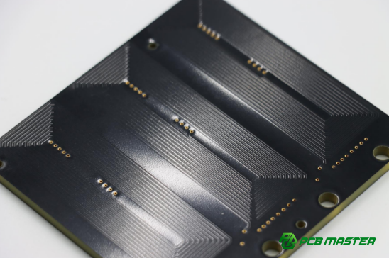
A Printed Circuit Board (PCB) is a crucial component in modern electronics, providing the physical platform for connecting and supporting electrical components like resistors, capacitors, and chips. PCBs are used in almost all electronic devices, from smartphones to medical equipment, ensuring the circuits inside work properly. At the heart of a PCB's design are vias, small holes that create electrical connections between different layers of the board. In multi-layer PCBs, which have multiple layers of circuitry stacked on top of each other, vias allow the electrical signals to pass between these layers, enabling the functionality of complex devices.
One method to enhance the performance of vias is by filling them with copper paste. This technique involves filling the vias with a special paste made of copper powder and resin. Copper paste helps improve the electrical conductivity, heat dissipation, and overall mechanical strength of the PCB. By using copper-filled vias, manufacturers can create more reliable and efficient PCBs, particularly in high-speed or high-power applications. This article will explore how copper paste is used in via filling, its benefits, and why it plays a key role in modern PCB manufacturing.
What Does "Via Filled with Copper Paste" Mean?
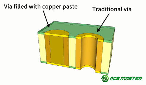
"Via filled with copper paste" means filling the holes (vias) in a PCB with a copper-based paste to enhance electrical conductivity, heat dissipation, and mechanical strength.
Definition of Via in PCB Context
In PCB design, a via is a small hole that connects different layers of a PCB. These holes allow electrical signals to pass from one layer of circuitry to another. Without vias, a multi-layer PCB would not be able to function properly because the components on different layers wouldn't be able to communicate.
There are several types of vias:
l Through-hole vias: These are the most common and run through the entire thickness of the PCB, connecting all the layers.
l Blind vias: These connect an outer layer to an inner layer but do not go all the way through the board.
l Buried vias: These connect only inner layers of a PCB and do not reach the outer surface. They are typically used in high-density designs.
Each type of via serves a specific purpose depending on the design requirements of the PCB.
What is Copper Paste?
Copper paste is a specialized material made by suspending fine copper powder in a resin solution. This paste is used to fill vias in PCBs, offering a conductive solution that enhances the performance of the PCB. Unlike traditional copper plating, which involves electroplating a thin layer of copper over the surface of the PCB, copper paste is applied directly into the via holes. After application, the paste is cured, solidifying into a robust copper structure.
The main advantage of copper paste over traditional methods is that it fills the vias more effectively, ensuring better electrical conductivity and thermal performance. It also provides a more cost-effective and reliable solution for high-speed, high-frequency, and power-intensive circuits. Copper paste can be applied quickly and efficiently in manufacturing, making it an attractive option for both large-scale and specialized PCB production.
What Are the Benefits of Using Copper Paste in Via Filling?
The benefits of using copper paste in via filling include improved electrical conductivity, enhanced heat dissipation, better signal integrity, increased mechanical strength, and cost-effective manufacturing, especially in high-performance and high-density PCBs.
Improved Electrical Conductivity
Copper paste significantly improves the electrical connections in vias by offering better conductivity compared to traditional methods like copper plating. When copper paste is used to fill vias, it creates a solid, continuous copper connection through the hole, ensuring minimal resistance.
| Method | Electrical Conductivity | Description |
| Copper Paste Filling | High | Provides a solid copper connection, ensuring low resistance. |
| Copper Plating | Moderate | Copper plating can result in some inconsistencies in the via connection, increasing resistance. |
| No Filling | Low | Unfilled vias lead to higher resistance, reducing overall electrical performance. |
Copper paste reduces via resistance by filling the entire via with conductive material, eliminating gaps or voids that can increase resistance and reduce signal flow.
Enhanced Heat Dissipation
Copper paste improves heat management in PCBs, especially in high-power or high-frequency applications. The copper-filled vias act as thermal conductors, helping dissipate heat away from sensitive components. In power electronics, where heat generation is a common issue, using copper paste to fill vias is especially beneficial. For example, in power supplies, the copper paste helps maintain the PCB's temperature, preventing overheating and damage to critical components. This heat-dissipation property is vital in preventing thermal-related failures in high-performance devices.
Better Signal Integrity
Copper paste improves signal integrity by reducing signal loss, crosstalk, and impedance mismatches in vias. The continuous copper connection in filled vias ensures a smoother signal path, resulting in faster and more reliable signal transmission. This is particularly important in high-speed and high-frequency circuits, such as 5G and RF (Radio Frequency) devices. For instance, in 5G antennas, copper-filled vias reduce signal degradation, ensuring clearer communication and more efficient data transmission. This makes copper paste a crucial component in the design of modern, high-performance PCBs.
Increased Durability and Mechanical Strength
Copper paste enhances the mechanical integrity of PCBs by providing extra strength to vias, making them more resistant to mechanical stress and thermal cycling. In environments where PCBs are exposed to frequent temperature changes, such as in automotive or industrial applications, copper-filled vias prevent cracking and failure. This increases the long-term reliability of the PCB, ensuring it performs well even under harsh conditions. The added strength also prevents physical damage during manufacturing processes, such as drilling or handling.
Cost-Effective Manufacturing
Copper paste filling is more cost-effective than traditional copper plating or other via treatments, particularly for low- to mid-volume PCB production. Unlike copper plating, which requires expensive electroplating equipment and processes, copper paste can be applied quickly and efficiently using standard manufacturing tools. This makes it an attractive option for companies looking to reduce production costs without compromising quality.
| Method | Cost | Benefits |
| Copper Paste Filling | Low | Cost-effective for small to medium batches, requires less complex equipment. |
| Copper Plating | High | Expensive due to the need for electroplating setup and longer production time. |
| No Filling | Very Low | Cheapest option, but results in reduced performance. |
Copper paste also reduces the need for additional processes, making it a more economical choice for high-performance applications without increasing manufacturing complexity.
What Are the Applications of Via Filled with Copper Paste in PCB Manufacturing?
Via filled with copper paste is used in high-power and high-frequency circuit boards, advanced multi-layer PCBs, and miniaturized, high-density PCBs to improve electrical conductivity, heat dissipation, signal integrity, and overall performance.
High-Power and High-Frequency Circuit Boards
Copper-filled vias are highly beneficial in high-power and high-frequency circuit boards. These vias play a key role in handling high currents and enabling fast signal transmission by providing low-resistance, highly conductive paths between PCB layers. Copper paste significantly enhances the thermal conductivity of the vias, which is crucial in preventing overheating in power-intensive circuits.
For instance, in power supplies, the copper-filled vias help effectively manage heat generation, preventing components from getting damaged due to excessive temperature rise. Similarly, in RF (Radio Frequency) and microwave circuits, the enhanced signal integrity from copper-filled vias reduces signal loss and interference, ensuring smooth data transmission in devices like antennas and communication equipment. The increased efficiency of copper-filled vias ensures that high-speed and power-sensitive circuits perform optimally without overheating or signal degradation.
Advanced Multi-layer PCBs
Copper paste improves the functionality of multi-layer PCBs by enhancing both electrical and thermal performance. In multi-layer designs, copper-filled vias connect the different layers of the PCB and allow signals to flow seamlessly between them. The copper paste increases the thermal conductivity of these vias, helping the board dissipate heat more effectively, which is especially important in complex circuits where heat buildup can lead to failure.
For example, in automotive electronics, copper-filled vias are used in high-performance systems such as electric vehicle (EV) power management and advanced driver-assistance systems (ADAS). Similarly, in medical devices, like MRI machines or patient monitoring systems, copper paste improves heat management and signal integrity, ensuring long-term reliability in critical applications. In both these sectors, where failure is not an option, copper-filled vias provide essential support to the PCB's functionality.
Miniaturized and High-Density PCBs
In miniaturized and high-density PCBs, such as those found in smartphones and wearables, copper-filled vias help maintain signal integrity and improve overall board performance. As these devices become smaller and more compact, maintaining electrical and thermal efficiency in a limited space becomes more challenging. Copper paste ensures that vias provide high conductivity, even in high-density designs, without taking up too much physical space.
The use of copper-filled vias in miniaturized designs prevents signal loss and interference that could affect the device's performance. For example, in smartphones, where multiple circuits and antennas are packed into a small area, copper paste ensures the efficient transmission of signals while also managing heat generation from the compact, power-hungry components. Similarly, wearables such as smartwatches benefit from copper-filled vias, as they maintain high-speed data processing and longer-lasting performance without overheating.
How is Copper Paste Used in Via Filling During PCB Manufacturing?
Copper paste is used in via filling during PCB manufacturing by injecting the paste into drilled vias, curing it to create a solid copper connection, and ensuring improved electrical conductivity and heat dissipation between layers.
Manufacturing Process Overview
The process of filling vias with copper paste involves several steps, each critical to ensuring a strong, reliable, and conductive connection within the PCB. Here's a step-by-step breakdown:
1. Drilling the Vias: The first step is to drill small holes (vias) through the PCB. These holes are designed to connect different layers of the PCB to allow electrical signals to pass between them. Vias can be drilled using specialized machines that ensure precise hole sizes and depths.
2. Cleaning and Prepping Vias: After drilling, the vias are thoroughly cleaned to remove any debris, dust, or oils. This cleaning process ensures that the copper paste adheres properly to the surfaces of the vias. Vias are also prepped by applying a thin layer of surface treatment to enhance adhesion.
3. Applying Copper Paste: Next, copper paste is carefully injected into the vias. The paste, made of fine copper powder suspended in resin, is applied using a precise injection process to ensure that each via is completely filled. This paste is carefully distributed to fill the entire hole.
4. Curing and Hardening Process: After the copper paste is applied, the PCB goes through a curing process. The copper paste is heated in an oven to harden it, creating a solid copper connection within the via. The heat causes the resin to bond with the copper powder, ensuring the vias are filled and solidified.
5. Final Inspection and Testing: Once the copper paste is fully cured, the board undergoes a final inspection. This includes checking the quality of the via filling for any voids or imperfections. The PCB is then tested to ensure electrical continuity and overall functionality.
Technology and Equipment Involved
The process of copper paste via filling requires advanced technology and specialized equipment to ensure accuracy and efficiency.
1. Paste Injection Systems: These are precision machines used to inject copper paste into the vias. The system is designed to control the amount of paste used, ensuring uniform filling across all vias. These machines are often automated to speed up the production process and improve consistency.
2. Curing Ovens: After the paste is injected into the vias, curing ovens are used to heat the boards at a controlled temperature. This process solidifies the copper paste, transforming it from a semi-liquid state to a solid copper conductor. The curing process is crucial for ensuring the durability and strength of the filled vias.
3. Innovations in Via Filling Technology: As PCB manufacturing continues to evolve, innovations in via filling technology have focused on improving the quality, efficiency, and scalability of the process. For instance, some companies have developed high-speed paste injection systems that minimize the time required for filling vias, while others use advanced curing techniques to ensure even distribution of heat and consistent paste hardening. These innovations help manufacturers produce higher-quality PCBs faster and at a lower cost.
In summary, copper paste via filling is an essential part of PCB manufacturing, using specialized equipment like paste injection systems and curing ovens to ensure high-quality connections between layers. Innovations in this technology continue to improve efficiency and quality in PCB production.
What Are the Challenges of Using Copper Paste for Via Filling?
The challenges of using copper paste for via filling include ensuring consistent, void-free filling for reliable electrical connections and addressing material compatibility issues with other PCB components to avoid poor adhesion or performance.
Consistency and Quality Control
One of the biggest challenges of using copper paste for via filling is ensuring consistent filling and preventing defects like voids or incomplete fills. Voids occur when the paste does not completely fill the via, creating gaps in the copper connection. These gaps can lead to higher resistance, weak electrical connections, and even PCB failure under high stress. Inconsistent filling can also result in uneven heat dissipation, leading to hotspots and overheating in the final product.
Ensuring uniform filling is crucial for maintaining the reliability of the PCB. If the vias are not properly filled, the overall performance of the circuit can degrade. This may cause electrical failures, signal loss, and even mechanical damage in critical applications like medical devices or automotive electronics, where failure is unacceptable. Quality control measures such as automated inspection, X-ray imaging, and resistance testing are essential to detect and address filling inconsistencies before the PCB is finalized.
Material Compatibility
Another challenge with copper paste is ensuring material compatibility with the other components used in PCB manufacturing. Copper paste must adhere properly to the via walls to create a solid connection. If the paste does not bond well to the PCB material, such as the base layer or coating, it can result in poor conductivity and weak vias.
In addition, copper paste may interact with other materials on the PCB, such as solder mask or other layer coatings, causing adhesion issues or even damaging the layers. These issues are especially relevant when designing for different substrates or specific component types. For example, PCBs with sensitive components like capacitors or integrated circuits may require special design considerations to ensure the copper paste does not interfere with component performance. Manufacturers must carefully select compatible materials and optimize the design to avoid potential issues, ensuring that the copper paste performs as intended without compromising the integrity of the PCB.
Best Practices for Via Filling with Copper Paste in PCB Design
Best practices for via filling with copper paste in PCB design include optimizing via size and placement for efficient filling, and implementing strict process control and quality assurance measures, such as automated filling systems and regular inspections, to ensure consistent and reliable results.
Optimizing Via Size and Placement
Optimizing the size and placement of vias is crucial for effective copper paste filling. The larger the via, the more copper paste is required, which can lead to filling challenges such as voids or incomplete filling if not done carefully. It's important to strike the right balance between via size and the amount of paste needed for a uniform fill.
When designing for optimal via filling, the following guidelines should be followed:
1. Via Size: Keep vias as small as possible to minimize the amount of paste required while still maintaining functionality. Smaller vias also help reduce the chances of defects in filling.
2. Via Placement: Place vias in locations that minimize stress on the paste during curing. Avoid placing vias too close to components or edges, as this can result in poor paste adhesion or uneven curing.
3. Layer Configuration: In multi-layer PCBs, ensure that vias are placed in areas where multiple layers can benefit from the copper paste filling. Well-distributed vias across layers improve thermal and electrical performance.
By carefully optimizing via size and placement, you ensure that the copper paste is evenly distributed and fills the vias efficiently, improving the overall quality of the PCB.
Process Control and Quality Assurance
Ensuring process control and quality assurance is vital for maintaining consistent copper paste filling. The filling process must meet strict standards for precision and consistency to prevent defects and ensure reliable performance in the final PCB.
To achieve high-quality results:
1. Automated Filling Systems: Use automated systems to inject the copper paste accurately into the vias. These systems can monitor paste distribution in real-time, ensuring uniformity across all vias.
2. Quality Checks: Implement X-ray inspection and electrical testing to detect voids, incomplete fills, or any inconsistencies in the copper paste application. These quality checks are essential to guarantee that vias are fully filled with copper paste and that the PCB will perform as expected under operational conditions.
3. Key Performance Indicators (KPIs): KPIs such as via fill percentage, thermal conductivity, and electrical continuity should be regularly monitored. By tracking these KPIs, manufacturers can assess the quality of the copper paste filling process and identify any areas for improvement.
By focusing on process control and maintaining strict quality standards, manufacturers can ensure that copper-filled vias perform optimally and meet the reliability standards required for high-performance PCBs.
Conclusion
In modern PCB manufacturing, via filling with copper paste plays a crucial role in enhancing the electrical conductivity, heat dissipation, and mechanical strength of PCBs. This technique offers significant benefits, including improved performance, durability, and cost-effectiveness, particularly for high-power, high-frequency, and miniaturized designs. By ensuring uniform and reliable filling, copper paste enhances signal integrity, prevents overheating, and increases the longevity of PCBs, making it an essential method in the production of high-quality electronics.
Looking ahead, the future of via filling technologies holds exciting potential. Innovations in copper paste formulations, such as enhanced copper powder blends and more efficient curing processes, will continue to drive improvements in thermal management, electrical performance, and manufacturing efficiency. These advancements will allow for even more compact, reliable, and high-performance PCBs, meeting the demands of emerging technologies.
As a trusted PCB and PCBA supplier, PCBMASTER is committed to providing high-quality products tailored to meet the evolving needs of the electronics industry. With years of experience in PCB manufacturing, PCBMASTER ensures that each product is crafted with precision, using the latest technologies to deliver superior performance, reliability, and value. Whether for small-scale prototypes or large-volume production, PCBMASTER is your trusted partner for all PCB and PCBA needs.
FAQs
1. What are the advantages of using copper paste over traditional via filling methods?
Using copper paste for via filling offers several advantages over traditional methods like copper plating or no filling at all.
l Enhanced Electrical Conductivity: Copper paste provides a solid and continuous copper connection in vias, resulting in lower resistance compared to traditional methods, which can have inconsistent filling or plating.
l Better Heat Dissipation: Copper-filled vias are excellent at transferring heat, which helps prevent overheating of the PCB, especially in high-power applications where heat buildup can damage components.
l Increased Mechanical Strength: Copper paste strengthens the mechanical integrity of the vias, making them more resistant to thermal expansion and mechanical stress, which is particularly useful in high-frequency and high-power circuits.
These benefits ensure that copper paste via filling improves both the reliability and performance of PCBs, making it an ideal solution for demanding applications.
2. Can copper paste filling be used for all types of PCBs?
Copper paste filling is particularly beneficial for certain types of PCBs, especially those that require enhanced electrical and thermal performance:
l Multi-layer PCBs: These boards benefit significantly from copper-filled vias, as they help ensure better signal integrity, reduce heat buildup, and connect multiple layers of the PCB with minimal resistance.
l High-Power PCBs: Copper paste improves the ability of the vias to handle high currents, making them essential for power-intensive applications like power supplies or power amplifiers.
l High-Frequency PCBs: For circuits that process high-speed signals, such as RF or 5G devices, copper-filled vias reduce signal degradation, ensuring stable and reliable operation.
While copper paste is most advantageous for high-performance PCBs, it may not be necessary for simpler, low-performance boards where cost and basic functionality are more important.
3. How does copper paste filling impact the overall cost of PCB manufacturing?
Copper paste filling is cost-effective, especially for low to mid-volume production. While traditional copper plating processes require expensive equipment for electroplating, copper paste can be applied using more affordable systems, reducing production costs.
l Lower Equipment Costs: The process of filling vias with copper paste is less complex and requires less specialized equipment compared to traditional copper plating, leading to lower capital investment.
l Reduced Material Waste: Copper paste is applied directly to the vias, reducing material waste compared to traditional plating, where excess copper can often be removed.
l Faster Production: The copper paste filling process is typically faster, enabling quicker turnaround times and cost savings, especially for prototype or small-batch production.
Overall, copper paste filling makes it possible to produce high-quality PCBs more affordably, especially for niche or low-to-mid volume applications.
4. Is there a risk of voids when using copper paste for via filling?
Yes, there is a risk of voids when using copper paste for via filling. Voids occur when the paste doesn't completely fill the via, leading to gaps in the copper connection. These voids can increase the electrical resistance of the via and cause issues with heat dissipation, which may result in PCB failure under high stress.
To minimize voids:
l Proper Process Control: Ensure the paste is evenly distributed and the vias are completely filled during the application process. Automation and precision in filling help prevent voids.
l Curing Process: The curing process must be carefully controlled to ensure that the copper paste solidifies uniformly, eliminating gaps.
l Quality Assurance: Regular inspections, such as X-ray imaging and resistance testing, can detect voids and other imperfections before the PCB reaches the final stages.
Addressing the risk of voids ensures that copper paste filling provides reliable and consistent performance.
5. What industries benefit the most from copper-filled vias in PCBs?
Several industries rely heavily on copper-filled vias in PCBs due to their performance, durability, and reliability:
l Automotive: Copper-filled vias are crucial for automotive PCBs used in electric vehicles (EVs), advanced driver-assistance systems (ADAS), and other critical automotive electronics, where performance and durability in harsh environments are vital.
l Telecommunications: High-frequency communication devices, such as 5G antennas and routers, benefit from copper-filled vias, as they ensure excellent signal integrity and heat dissipation in high-speed circuits.
l Medical Devices: In medical electronics, such as patient monitoring systems or diagnostic equipment, copper-filled vias provide the reliability and long-term performance required for critical applications, where failure can have serious consequences.
In these industries, copper-filled vias are essential for ensuring the high reliability, efficient heat management, and long-term durability needed for complex and mission-critical systems.
Author Bio
Hi, I'm Carol, the Overseas Marketing Manager at PCBMASTER, where I focus on expanding international markets and researching PCB and PCBA solutions. Since 2020, I've been deeply involved in helping our company collaborate with global clients, addressing their technical and production needs in the PCB and PCBA sectors. Over these years, I've gained extensive experience and developed a deeper understanding of industry trends, challenges, and technological innovations.
Outside of work, I'm passionate about writing and enjoy sharing industry insights, market developments, and practical tips through my blog. I hope my posts can help you better understand the PCB and PCBA industries and maybe even offer some valuable takeaways. Of course, if you have any thoughts or questions, feel free to leave a comment below—I'd love to hear from you and discuss further!

