


Understanding Solder Mask Thickness: Key Requirements and Best Practices for PCB Manufacturing
A printed circuit board (PCB) is only as reliable as its protective layers, and at the heart of this protection lies solder mask ink. Its thickness, often overlooked, plays a crucial role in ensuring durability, preventing shorts, and maintaining electrical integrity. Whether it's a consumer gadget or a complex aerospace component, understanding the nuances of solder mask thickness is essential for optimal performance. The balance between too thin and too thick can make all the difference, influencing everything from the board’s electrical reliability to its long-term durability. Let’s dive into why getting this just right is vital for the success of any electronic product.
Why is Solder Mask Ink Thickness Crucial?
Solder mask ink thickness is crucial because it protects the PCB from environmental damage, ensures proper electrical performance, and influences the board's long-term reliability.
Solder Mask Ink’s Role and PCB Protection
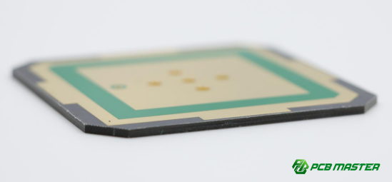
Solder mask ink plays a critical role in protecting the PCB from various external factors. It acts as a barrier against moisture, dust, and chemicals, which could otherwise cause corrosion or electrical damage. The ink also helps prevent short circuits by covering copper traces, ensuring that the only parts exposed to solder during the assembly process are the pads and leads. In simple terms, it is the shield that keeps the delicate components safe from environmental harm and manufacturing issues. Without a proper solder mask thickness, a PCB would be much more prone to failure, especially in harsh conditions.
Solder Mask Ink Thickness and Electrical Performance
The thickness of the solder mask ink has a direct impact on the electrical performance of the PCB. A solder mask that’s too thin can allow electrical leakage between traces, especially in high-voltage or high-speed applications. On the other hand, if the solder mask is too thick, it can cause unwanted signal interference or even damage sensitive components during soldering. For instance, in high-frequency boards, thin and uniform solder masks are necessary to maintain the board’s impedance and prevent signal distortion. Therefore, the right solder mask thickness is essential for optimal electrical performance, ensuring that the board functions as intended without compromising its electrical integrity.
Factors Influencing Product Reliability
Several factors determine the overall reliability of a PCB, and solder mask thickness is one of the most important. When the thickness is not controlled properly, it can lead to several issues, such as weak adhesion between the mask and the PCB, which may result in cracking or peeling over time. Furthermore, inadequate thickness can also increase the likelihood of soldering defects, such as bridging or poor wetting. Reliability is especially critical in products subjected to extreme environments, such as automotive electronics or medical devices. In these cases, the solder mask must be thick enough to withstand temperature fluctuations, vibrations, and exposure to chemicals, all of which can compromise a thin mask.
Solder Mask Ink Thickness Standards and Requirements
Solder mask ink thickness standards ensure the PCB’s protection, electrical performance, and reliability by specifying required thickness ranges based on product type, with different applications such as automotive electronics demanding thicker masks for durability and performance.
What Are the IPC Standards for Solder Mask Thickness?
The IPC standards for solder mask thickness, outlined in IPC-SM-840 and IPC-6012, define minimum thickness requirements based on product reliability, with specific guidelines for various applications, such as consumer electronics, automotive, and high-voltage products.
Overview of IPC-SM-840 and IPC-6012 Standards
The IPC-SM-840 and IPC-6012 are industry standards that define the minimum requirements for solder mask performance and the quality of rigid PCBs. IPC-SM-840 focuses on the evaluation and performance of the solder mask material itself, while IPC-6012 sets the standards for the quality and reliability of the entire PCB, including the solder mask. These standards outline acceptable limits for solder mask thickness to ensure that the board performs reliably in various environments. Adhering to these standards helps manufacturers maintain high-quality products that meet the necessary operational and safety requirements.
Specific Thickness Requirements and Product Type Relationships
Different product types require different solder mask thicknesses based on their intended use. For example, consumer electronics typically have a thinner solder mask (around 10-15 microns) as they are designed for low-stress applications. On the other hand, automotive and industrial products often need thicker solder masks (15-40 microns) to withstand harsher conditions like vibration, heat, and chemicals. The IPC standards take these factors into account by providing specific thickness recommendations for different categories of products, ensuring that the PCB will perform as expected throughout its lifespan.
Definition of Minimum Local Thickness in Standards
The IPC standards also specify the minimum local thickness of the solder mask, which refers to the thinnest point in the entire solder mask layer after curing. This is an important measure because it ensures that the solder mask provides consistent protection across the PCB, without weak spots that could lead to electrical shorts or other failures. For instance, IPC-SM-840 emphasizes that the minimum thickness should not fall below a certain micron level, which varies depending on the type of PCB and its application. Ensuring that the solder mask meets this requirement is crucial for maintaining long-term reliability and performance.
What Are the Solder Mask Thickness Requirements for Automotive Electronics?
Solder mask thickness requirements for automotive electronics typically range from 15 to 40 microns to ensure robust insulation and protection against extreme conditions like temperature cycles, vibration, and chemical exposure.
Special Requirements for Automotive Standards
Automotive electronics must meet stringent durability and reliability standards due to the extreme environments they are exposed to, such as fluctuating temperatures, vibrations, and exposure to chemicals. Automotive standards, like those set by the International Organization for Standardization (ISO) and the automotive industry’s specific requirements, typically demand a thicker solder mask to protect the components. The solder mask must ensure that the PCB remains operational even under challenging conditions, including high humidity, road salt, and engine heat. Therefore, automotive electronic products often require a solder mask thickness between 15μm and 40μm to provide adequate protection.
Function of Solder Mask in Automotive Electronics
In automotive electronics, the solder mask serves multiple purposes. It prevents electrical shorts by covering the PCB’s copper traces, reduces the risk of corrosion from environmental exposure, and offers mechanical protection against wear and tear. The solder mask also plays a crucial role in ensuring the integrity of the board during the soldering process by preventing solder bridges and maintaining clean pads for component attachment. Given the harsh conditions, the solder mask must have excellent adhesion to the PCB and maintain its protective qualities over time, ensuring the electronics function properly for years.
Thickness Range: 15μm ~ 40μm in Practical Applications
In practical applications, automotive electronics typically use solder masks in the range of 15μm to 40μm. This thickness range ensures the solder mask is thick enough to protect the PCB from extreme temperatures, moisture, and chemicals but not so thick that it interferes with the manufacturing process or performance of small, dense components. For example, thicker masks help prevent issues such as microcracking, which could be caused by thermal cycling, while thinner masks are used in areas where components are closely spaced. This range also helps maintain the PCB’s electrical performance by preventing impedance mismatch or signal degradation.
Factors Affecting Solder Mask Ink Thickness
Solder mask ink thickness is influenced by coating techniques like screen printing, spray coating, and electrostatic spray, as well as the type of ink used, such as Liquid Photoimageable (LPI) or thermosetting inks, each affecting the final thickness and uniformity of the layer.
How Do Different Coating Techniques Affect Solder Mask Thickness?
Different coating techniques, such as screen printing, spray coating, and electrostatic spray, affect solder mask thickness by offering varying levels of control, with screen printing generally producing thicker layers and spray methods achieving thinner, more uniform coatings.
Screen Printing and Thickness Control
Screen printing is one of the most common methods for applying solder mask ink on a PCB. It allows for precise control over the thickness of the applied layer, which typically ranges from 20-40 microns. The thickness is controlled by adjusting the mesh size of the screen and the pressure applied during printing. This method is well-suited for thicker applications, making it ideal for industrial or automotive PCBs that require more robust protection. However, it’s important to ensure consistent pressure and screen quality to avoid variations in thickness, which could impact the board's electrical and mechanical properties.
Spray Coating Technology and Uniform Thin Layers
Spray coating, including techniques like automated spray systems, is used when a thinner and more uniform solder mask is required. This method generally results in a thinner layer, typically ranging from 10-25 microns, and is ideal for high-density, smaller-pitch boards where excess thickness could cause issues with component placement or signal integrity. Spray coating provides good coverage, but the uniformity can depend on the spray settings and the environment in which it is applied, such as temperature and humidity. Proper control of these factors ensures that the solder mask layer remains consistent and protective.
Electrostatic Spray Coating: Advantages and Applications
Electrostatic spray coating is a more advanced version of traditional spray coating, where the solder mask ink is charged and sprayed onto the PCB. This method ensures excellent coverage, especially on complex shapes and tight spaces, and is often used in high-density boards. The electrostatic charge helps the ink adhere more evenly, leading to a more consistent thickness. This method is highly effective for thin layers (10-20 microns) and is particularly useful in applications where the PCB has very tight component spacing or where high-performance electrical characteristics, like signal integrity, are essential.
How Does Ink Type Affect Solder Mask Thickness?
The ink type affects solder mask thickness by determining its consistency and curing properties, with Liquid Photoimageable (LPI) inks typically producing thinner, uniform layers, while thermosetting inks result in thicker, more durable coatings.
Characteristics of Liquid Photoimageable Ink and Thickness Control
Liquid Photoimageable (LPI) ink is one of the most common types of solder mask ink used in PCB manufacturing. It is highly versatile, offering excellent resolution and uniformity in thickness, typically ranging from 15-30 microns. The thickness of LPI ink can be controlled by adjusting the exposure time and curing conditions during the photolithography process. LPI ink is preferred for high-density boards because of its ability to produce a thin and consistent layer that does not interfere with the board’s functionality. Its key advantage is the ability to achieve a precise, smooth finish, which is essential for modern electronics like smartphones and computers.
Thickness Variations with Thermosetting Inks and Their Applications
Thermosetting inks, unlike LPI inks, undergo a chemical curing process when heated, resulting in a more rigid and thicker solder mask. Typically applied through screen printing, these inks tend to produce a thicker layer, ranging from 30-40 microns. The thickness variation in thermosetting inks can be more significant, depending on curing temperature and time, and may lead to issues with uniformity if not controlled properly. However, they are ideal for applications where the solder mask needs to withstand harsher environments, such as automotive or industrial PCBs, where higher protection against physical wear, chemicals, and heat is required.
Solder Mask Thickness Requirements for Different Product Categories
Solder mask thickness requirements vary by product category, with consumer electronics needing thinner layers (10-15 microns) for basic protection, while industrial, high-voltage, aerospace, and high-frequency products require thicker layers (15-40 microns) for enhanced durability, electrical insulation, and signal integrity.
How Thick Should Solder Mask Ink Be for Consumer Electronics?
Solder mask ink for consumer electronics should typically be between 10 to 15 microns thick to provide basic insulation and protection without interfering with high-density components.
Basic Insulation and Protection Requirements
Consumer electronics typically require a thinner solder mask layer, as the primary function is to provide basic insulation and protection against dust, moisture, and soldering defects. The solder mask prevents short circuits and leakage by covering the copper traces, ensuring reliable performance in everyday conditions. However, the demands are not as extreme as in industrial or automotive applications, so a thinner layer is sufficient for most consumer electronics, like smartphones, tablets, and laptops.
Common Thickness Range and Process Selection
For consumer electronics, the typical solder mask thickness range is between 10-15 microns. This thickness is ideal for providing the necessary insulation and mechanical protection without adding excess material that could interfere with high-density components or manufacturing processes. Liquid Photoimageable (LPI) ink is commonly used for this purpose, as it can be applied with high precision, creating a thin, uniform layer. The use of screen printing or spray coating methods ensures the right thickness and uniformity needed for these high-tech products.
What Are the Solder Mask Thickness Requirements for Industrial Control and Communication Equipment?
Solder mask thickness for industrial control and communication equipment typically ranges from 15 to 20 microns to ensure durability, environmental protection, and long-term reliability in harsh conditions.
Environmental Adaptability and Long-Term Reliability Requirements
Industrial control systems and communication equipment must operate reliably under more challenging conditions compared to consumer electronics. These environments may include temperature extremes, exposure to chemicals, and mechanical vibrations. Therefore, these applications demand a solder mask layer that is not only thick enough to protect the PCB but also capable of enduring these harsh environments over extended periods. The solder mask must offer long-term protection against environmental stress, corrosion, and physical damage.
Strict Thickness Control and Common Applications
For industrial and communication equipment, solder mask thickness typically ranges from 15-20 microns. This range ensures durability while maintaining functionality. It's important that the thickness is strictly controlled to avoid variations that could lead to weak points, especially in high-vibration or heavy-duty machinery. Solder masks in these applications often use thermosetting inks to ensure that the layer adheres strongly and provides additional protection against physical stress and chemical exposure.
What Are the Solder Mask Thickness Requirements for High Voltage and High-Voltage Products?
Solder mask thickness for high voltage and high-voltage products typically ranges from 25 microns and higher to provide adequate insulation, prevent arcing, and increase creepage distance.
Increasing Creepage Distance and Preventing Arc Breakdown
High voltage and high-voltage products require thicker solder mask layers to prevent electrical arcing and breakdown. A thicker solder mask increases the creepage distance, which is the distance that electrical current must travel across the surface of the board to jump from one conductor to another. This added distance reduces the risk of electrical shorts, especially in environments where high voltages could cause dangerous failures. Ensuring that the solder mask is thick enough helps prevent arcing under high voltage conditions.
Core Design Considerations for Thickness
For high voltage applications, solder mask thickness typically ranges from 25 microns and higher. The core design consideration is to create a protective layer thick enough to maintain electrical insulation between high-voltage components and other parts of the PCB. The solder mask must be carefully chosen to ensure that it can withstand the stresses of high voltage without degrading or becoming brittle over time. Additionally, thermosetting inks are often used to meet these strict requirements, as they can offer more robust protection in demanding conditions.
What Are the Solder Mask Thickness Requirements for Aerospace and Military Products?
Solder mask thickness for aerospace and military products typically exceeds 25 microns, with an emphasis on high uniformity and robust protection against extreme environments.
Extremely High Thickness Requirements and Uniformity
Aerospace and military applications demand the highest levels of reliability, so solder mask thickness must be carefully controlled to meet strict standards. These products often operate in extreme environments, including high altitudes, extreme temperatures, and exposure to radiation. For this reason, the solder mask layer must be both thick and uniform to ensure that it performs reliably under these conditions. Any variation in thickness can lead to failures, which is particularly dangerous in mission-critical systems.
Specialized Environmental Protection and Reliability
Solder mask thickness for aerospace and military applications typically ranges from 25 microns to higher. The primary concern is ensuring that the solder mask offers protection against environmental factors such as temperature fluctuations, vibration, and exposure to corrosive elements. These products also require the solder mask to resist thermal shock, radiation, and other stress factors. In this case, thermosetting inks are commonly used for their superior adhesion and robustness, ensuring a reliable protective layer.
What Are the Solder Mask Thickness Requirements for High-Frequency and High-Speed Products?
Solder mask thickness for high-frequency and high-speed products typically ranges from 8 to 20 microns, with a focus on uniformity to maintain signal integrity and consistent impedance.
Impedance Continuity for Signal Transmission
High-frequency and high-speed products require extremely precise solder mask thickness to maintain signal integrity. The solder mask must be thin enough to prevent signal degradation, as any variation in thickness can lead to changes in impedance, disrupting signal transmission. In high-speed electronics, such as those used in telecommunications or data centers, maintaining consistent impedance is essential for ensuring fast and reliable signal flow across the PCB.
Uniform Control of Thin Layers
For high-frequency and high-speed applications, solder mask thickness is generally kept within a range of 8-20 microns. The key requirement is achieving a uniform layer thickness, which is critical for maintaining consistent electrical characteristics across the board. Even small variations can lead to significant problems with signal integrity. To ensure this, spray coating or electrostatic spray coating is commonly used to create a thin, consistent layer. This is particularly important in RF (Radio Frequency) circuits, where the slightest deviation in solder mask thickness can lead to signal distortion or data loss.
Problems Caused by Insufficient Solder Mask Thickness
Insufficient solder mask thickness can lead to insulation breakdown, soldering defects, reduced mechanical protection, increased risk of CAF, and visual defects, ultimately compromising the PCB's performance, reliability, and customer acceptance.
How Does Insufficient Solder Mask Thickness Affect PCB Insulation?
Insufficient solder mask thickness compromises PCB insulation by increasing the risk of insulation breakdown, leakage, and short circuits, especially under high humidity or electrical stress.
Risk of Insulation Breakdown and Leakage
When the solder mask thickness is too thin, it can fail to provide sufficient electrical insulation, increasing the risk of insulation breakdown. This occurs when the protective layer is too weak to withstand electrical stress, allowing current to pass through unintended areas. As a result, electrical leakage can occur between copper traces or from the traces to the PCB's surface, leading to shorts, malfunctioning circuits, or even complete failure of the PCB. Thin solder masks are especially problematic in high-voltage applications, where proper insulation is essential to prevent short circuits or electric shocks.
Impact of High Humidity and Contamination on Thin Layers
Thin solder masks are more susceptible to the effects of high humidity and contamination. Moisture can easily penetrate a thin solder mask, causing the copper traces to corrode over time, reducing the PCB's lifespan and reliability. Additionally, dirt and chemicals can directly affect the performance of thin layers, leading to increased chances of leakage or electrical shorts. In environments where exposure to moisture or pollutants is high, such as in industrial or automotive applications, insufficient solder mask thickness may exacerbate these risks, resulting in frequent failures or performance degradation.
What Soldering Issues Are Caused by Weak Solder Mask Layers?
Weak solder mask layers can lead to solder bridging, solder ball formation, and poor adhesion, causing short circuits, defects, and compromised reliability during the soldering process.
Solder Bridging and Solder Balls Formation
A thin solder mask can lead to solder bridging and the formation of solder balls during the soldering process. When the solder mask is too weak, molten solder may flow beyond the pads, causing bridges between traces, which can result in short circuits. Similarly, weak adhesion between the mask and the PCB can cause cracks or gaps, allowing solder to flow into unintended areas, creating solder balls. These issues are particularly concerning during wave soldering or reflow soldering, where the solder mask’s protective capabilities are critical for guiding the molten solder to the correct locations.
Cracking Caused by Poor Ink Adhesion
If the solder mask layer is too thin or poorly applied, the ink may not properly adhere to the PCB. This can lead to micro-cracks or peeling of the solder mask, especially under thermal stress from repeated reflow soldering cycles. These cracks create weak points in the PCB's protective layer, allowing solder and contaminants to seep in, leading to further defects like solder bridging or electrical failure. In high-stress environments, such as those involving temperature fluctuations or mechanical vibrations, poor adhesion significantly reduces the PCB's long-term reliability.
How Does Insufficient Solder Mask Thickness Affect Mechanical Protection and Chemical Resistance?
Insufficient solder mask thickness reduces mechanical protection, making the PCB more vulnerable to physical damage, and compromises chemical resistance, leading to potential degradation from cleaning solvents or environmental exposure.
Reduced Physical Protection
Solder masks are essential for providing physical protection to PCB traces and components, particularly from scratches, abrasion, or dust. A thinner solder mask layer offers less protection, making the PCB more vulnerable to physical damage during handling, assembly, or operation. For example, in industrial environments where PCBs may be exposed to rough conditions or heavy machinery, a thin solder mask may result in exposed copper or damaged traces, leading to circuit failure or loss of functionality.
Inability to Resist Post-Assembly Chemical Cleaning
During PCB assembly, cleaning processes are often required to remove flux residues or other contaminants. A thin solder mask may not be able to withstand the chemical solvents used in these cleaning processes, causing the mask to degrade, peel, or lose its protective qualities. This can result in corrosion of the PCB traces or exposure of sensitive components to harmful chemicals, which affects the performance and lifespan of the device. PCBs with thicker solder masks are better equipped to endure these cleaning processes without losing their protective properties.
How Does Insufficient Solder Mask Thickness Increase the Risk of CAF?
Insufficient solder mask thickness increases the risk of CAF (Conductive Anodic Filament) by allowing moisture and ions to migrate more easily along the PCB surface, leading to potential electrical shorts.
Causes and Effects of CAF (Conductive Anodic Filament)
CAF (Conductive Anodic Filament) is a phenomenon where ions migrate along the surface of a PCB under high temperature and humidity, causing an electrical short. A thin solder mask layer provides less resistance to this migration, increasing the chances of CAF formation. In the presence of moisture, ions can travel through the solder mask, following the path of least resistance, and create conductive filaments that lead to failures. CAF is especially problematic in high-reliability applications such as medical devices or aerospace electronics, where even small failures can have catastrophic consequences.
How Thickness Control Reduces CAF Risk
Controlling the solder mask thickness is crucial in reducing the risk of CAF. A thicker solder mask acts as a barrier to ion migration, preventing the formation of conductive filaments by sealing off potential pathways. By ensuring a uniform and adequate thickness (typically above 20 microns in high-reliability designs), manufacturers can effectively minimize the chances of CAF, especially in moisture-prone environments. Regular quality control during production ensures that the solder mask's thickness is consistently within the required range, reducing the risk of CAF and improving the overall reliability of the PCB.
How Does Insufficient Solder Mask Thickness Lead to Appearance Defects and Customer Acceptance Issues?
Insufficient solder mask thickness can cause uneven color, visual defects, and inconsistent coverage, leading to customer rejection based on strict appearance and quality standards.
Uneven Ink Color and Other Visual Defects
A thin or improperly applied solder mask layer can result in uneven color, bubbles, or shiny spots on the PCB surface. These visual defects are often a result of poor application, where the ink is too thin to provide uniform coverage. For products requiring precise aesthetics or strict visual standards, such as consumer electronics, these appearance issues can lead to customer dissatisfaction or product rejection. Consistent solder mask thickness is crucial for maintaining a professional and clean appearance.
Customer Acceptance Standards and Thickness Requirements
Most customers have strict acceptance criteria for PCB appearance, as outlined in industry standards like IPC-A-600. Thin solder masks that lead to visual defects may cause the product to fail inspection, resulting in costly rework or rejection. For industries with high visual standards, such as consumer electronics or automotive products, ensuring proper solder mask thickness is essential not only for functional reliability but also for meeting customer expectations regarding appearance and quality.
Control and Optimization of Solder Mask Ink Thickness
Controlling and optimizing solder mask ink thickness involves selecting the appropriate thickness based on application needs, setting clear design standards, and using quality control methods like screen printing and spray coating to ensure consistent, reliable performance.
How to Choose the Right Solder Mask Thickness?
The right solder mask thickness should be chosen based on the specific application requirements, such as environmental conditions, electrical performance, and product reliability, with thicker masks for harsh environments and thinner ones for high-density components.
Choosing the Right Thickness Based on Application Needs
The solder mask thickness should be chosen based on the specific application of the PCB. For example, consumer electronics often require a thinner solder mask layer, usually between 10-15 microns, to ensure basic protection and prevent short circuits. On the other hand, industrial and automotive applications, where the PCB is exposed to harsh environments, typically need thicker solder masks, ranging from 15-40 microns, for better durability and insulation. For high-voltage or aerospace applications, solder mask thickness might exceed 40 microns to provide enhanced protection and reliability under extreme conditions. By assessing the environment and performance requirements of the final product, manufacturers can select the appropriate solder mask thickness that ensures both functionality and reliability.
Setting Thickness Standards in PCB Design
In PCB design, defining the solder mask thickness standards early on is crucial for maintaining quality and ensuring the board performs as expected. Designers should establish these thickness specifications based on factors such as the component density, environmental conditions, and electrical demands of the product. For example, high-frequency circuits may require thinner layers to ensure signal integrity, while high-voltage applications need a thicker mask for insulation. These standards should be communicated clearly in design documentation to guide manufacturers in selecting the correct materials and applying the right processes for optimal results.
Quality Control Methods for Solder Mask Thickness
Quality control methods for solder mask thickness include monitoring printing parameters like mesh size and ink viscosity in screen printing, as well as using inspection tools like micrometers and profilometers to ensure uniformity in spray and electrostatic coating processes.
Thickness Control in Screen Printing
Screen printing is a widely used method for applying solder mask to PCBs. To ensure that the solder mask layer meets the required thickness, manufacturers need to carefully control the screen mesh size, printing pressure, and ink viscosity. Thicker masks can be applied by using a finer mesh and adjusting the printing speed to increase the ink volume. Conversely, for thinner layers, a coarser mesh and faster print speed may be used. Additionally, post-printing curing processes, such as UV exposure, should be optimized to ensure uniform curing and consistent thickness. Quality control in screen printing requires regular thickness measurements at various points across the PCB to ensure that the solder mask adheres to the specified standards.
Quality Inspection for Spray Coating and Electrostatic Spray Coating
Spray coating, including electrostatic spray, is often used for thin and uniform solder mask layers. To maintain consistent thickness, inspection tools like micrometers and profilometers are used to measure the solder mask layer at different locations on the PCB. Electrostatic spray coating helps achieve uniform coverage by charging the solder mask ink, which ensures even distribution across complex shapes. Regular visual inspection is also important for detecting any inconsistencies or defects, such as uneven coating or thick spots. Manufacturers often conduct tests like cross-sectioning to check the uniformity of the solder mask and its adhesion to the PCB. Both methods require stringent process control and regular quality checks to meet the required specifications and maintain reliable performance.
Conclusion
Maintaining the right solder mask thickness is essential for ensuring the functionality, durability, and aesthetic quality of PCBs across various applications. From consumer electronics to high-voltage and aerospace products, understanding the specific thickness requirements and implementing effective quality control measures can prevent costly defects and enhance product reliability. By selecting the right coating technique, ink type, and monitoring the thickness consistently, manufacturers can ensure that their PCBs meet the highest industry standards. For businesses looking to achieve superior results in PCB production and assembly, partnering with experienced suppliers like PCBMASTER can make a significant difference. With years of expertise in providing high-quality PCB and PCBA solutions, PCBMASTER is committed to delivering products that meet the exact specifications and exceed customer expectations.
FAQs
Does thicker solder mask ink always better?
While a thicker solder mask can provide better insulation and protection, it’s not always better. Overly thick solder mask layers can create stress points on the PCB, leading to potential cracking or delamination. Additionally, thicker solder masks can negatively affect high-density designs by interfering with the precise placement of components. For such designs, a thinner solder mask is often preferred to maintain integrity and component alignment. Therefore, the solder mask thickness must be carefully balanced to meet both electrical and mechanical requirements.
How do different coating techniques affect the choice of solder mask thickness?
Different coating techniques allow for varying degrees of thickness control. Screen printing is typically used for thicker solder mask layers, often ranging from 20 to 40 microns, which is suitable for applications requiring robust protection. This method provides good control over the thickness but can lead to thicker layers. Spraying and electrostatic spray coating, on the other hand, are better for achieving thinner, more uniform solder mask coatings, typically between 8 and 15 microns. These techniques are ideal for high-density boards where a thinner, even coating is necessary to avoid affecting the placement and performance of small components.
How can insufficient solder mask thickness be repaired?
Insufficient solder mask thickness can be repaired by applying additional layers of solder mask ink. This process typically involves re-coating the affected areas using the same ink or a different type to ensure proper coverage. Specialized repair techniques, such as laser direct imaging (LDI), can also be employed to add a thin, uniform layer in specific spots. After re-coating, it’s important to ensure the thickness is uniform across the entire PCB to maintain electrical insulation and mechanical protection. Additionally, post-repair curing processes like UV or thermal curing should be followed to ensure the solder mask fully hardens and bonds with the PCB surface.
Can increasing solder mask thickness improve PCB reliability?
Increasing solder mask thickness can improve PCB reliability by providing better insulation and protection against environmental factors such as moisture, dust, and chemicals. However, there are limits to how thick the solder mask can be. If the solder mask becomes too thick, it can lead to issues like thermal stress, cracking, or increased warping of the PCB. These factors can lead to poor solder joint integrity and affect the overall performance of the PCB. Therefore, while a thicker solder mask can enhance protection, it should be used in conjunction with design requirements and manufacturing constraints to avoid creating new reliability issues.
What is the relationship between solder mask thickness and PCB lifespan?
The solder mask thickness plays a significant role in the longevity of a PCB by providing electrical insulation and protecting the underlying copper traces from environmental damage. A properly applied solder mask reduces the risk of electrical leakage, short circuits, and corrosion, which can degrade the PCB over time. Additionally, it prevents soldering defects like solder bridges or flux residue buildup, which can compromise the PCB’s functionality. An optimal solder mask thickness helps ensure long-term reliability, reduces the likelihood of failure, and extends the PCB's service life in various operational environments.
Author Bio
Hi, I'm Carol, the Overseas Marketing Manager at PCBMASTER, where I focus on expanding international markets and researching PCB and PCBA solutions. Since 2020, I've been deeply involved in helping our company collaborate with global clients, addressing their technical and production needs in the PCB and PCBA sectors. Over these years, I've gained extensive experience and developed a deeper understanding of industry trends, challenges, and technological innovations.
Outside of work, I'm passionate about writing and enjoy sharing industry insights, market developments, and practical tips through my blog. I hope my posts can help you better understand the PCB and PCBA industries and maybe even offer some valuable takeaways. Of course, if you have any thoughts or questions, feel free to leave a comment below—I'd love to hear from you and discuss further!

