


What Is PCB Silkscreen? A Practical Guide to PCB Markings and Layout Rules
Small markings, big impact. PCB silkscreen directly affect assembly accuracy, inspection efficiency, and long-term maintenance. Clear silkscreen helps prevent polarity errors, speeds up troubleshooting, and makes every board easier to identify and manage. Get them wrong, and even a well-designed PCB can create avoidable production problems.
Here’s what you need to know about PCB silkscreen—and how to design them right.
What is PCB silkscreen?
PCB silkscreen is the printed identification layer on a PCB, often called silkscreen, legend, marking, or character layer.
Basic meaning of PCB characters, silkscreen, and markings
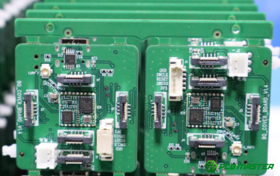
PCB characters are the letters, numbers, symbols, and simple graphics printed on the PCB surface. Common examples include R1, C2, U3, + / -, Pin 1 marks, and labels like USB1 or V1.0.
Common names include:
l PCB silkscreen: most common term
l PCB character layer: common in PCB design
l PCB marking: broader manufacturing term
l PCB legend: often used in documentation
These terms are closely related and often used interchangeably in searches like what is PCB silkscreen or PCB silkscreen meaning.
What is the difference between top silkscreen and bottom silkscreen?
Top silkscreen is usually the main labeling layer; bottom silkscreen is used only when needed.
| Item | Top Silkscreen | Bottom Silkscreen |
| Position | Top side of PCB | Bottom side of PCB |
| Main use | Component labels, polarity, connectors | Extra labels for bottom-side parts |
| Priority | High | Lower |
| Common use | Very common | Only when necessary |
Example: A single-sided assembly may only use top silkscreen. A double-sided board may add bottom silkscreen for bottom-side components or test points.
What are the main functions and key information of PCB silkscreen?
PCB silkscreen labels parts, shows polarity, marks interfaces and test points, and records board identity to support assembly, testing, and maintenance.
Component labels and reference designators
Silkscreen shows component labels like R1, C2, U3, and D4, making it easy to locate parts on the board. Each label matches the schematic and BOM. Common prefixes include:
l R for resistors
l C for capacitors
l U for ICs or chips
l D for diodes
Example: If the BOM specifies C7 = 10μF, the silkscreen label C7 ensures the correct capacitor is installed, reducing assembly errors and rework.
Polarity, orientation, and pin markings
Silkscreen shows the correct orientation for polarized components and IC pins, preventing installation mistakes. Common marks include:
l + / - for electrolytic capacitors
l Line mark for diode cathode
l Dot, notch, or triangle for IC Pin 1
Example: A reversed diode can short the circuit. Clear silkscreen marks prevent such errors during assembly and testing.
Tip: Align marks with the actual component placement for easy visual checking.
Board-level information and interface/test point labels
Silkscreen also records board identity and labels connectors for easy identification:
l Board info: board name (PCB-2025), version (V1.0/Rev B), production date, manufacturer code
l Interface/test points: USB1, J1, VCC, GND, TX, RX, TP1
Example: During debugging, an engineer can locate TP1 or GND quickly. Version info ensures the correct firmware or components are used for that PCB revision.
What key rules should be followed when designing PCB silkscreen?
PCB silkscreen must avoid covering pads, maintain readable sizes, and keep text direction and layout consistent to ensure assembly, inspection, and maintenance are easy and error-free.
Placement and clearance requirements
Silkscreen should never cover pads, vias, or test points, and must stay at a safe distance from components to avoid assembly problems.
Silkscreen overlapping a solder pad or via can block solder flow or create shorts. Maintain at least 0.2mm clearance from pads and test points. Avoid placing text under or too close to components, as it may be hidden after assembly.
Example: On a power board, marking R3 directly over a resistor pad can prevent proper soldering. Placing it slightly to the side ensures both visibility and soldering quality.
Size and readability requirements
Silkscreen must be large enough to read, with line widths thick enough to print clearly, even on high-density boards.
Typical recommendations:
l Standard boards: minimum text height ≥1.0mm, line width ≥0.15mm
l High-density boards: text height ≥0.8mm, line width ≥0.12mm
Using very small or thin fonts can cause blurred, broken, or illegible silkscreen. Always test text readability on the prototype board.
Example: A 0.6mm text height on a dense board may be unreadable after soldering. Increasing it to 0.8mm ensures clear identification of C12 and U5.
Consistent orientation and layout
All silkscreen text should face the same direction, and key labels should be placed where they are easy to see.
Consistent text orientation makes boards easier to inspect and assemble. Place critical marks like polarity symbols, IC Pin 1, and connectors in positions visible without moving the board or components.
Example: On a motherboard, aligning all reference designators from top-left to bottom-right allows assembly operators to read labels without rotating the board, speeding up production.
Which PCB silkscreen markings are critical and must be clearly visible?
Certain PCB silkscreen markings, such as polarity indicators, pin 1 marks for ICs, and board version information, are essential for proper assembly, testing, and maintenance.
Polarity markings for polarized components
Polarity markings ensure that components like capacitors, diodes, and LEDs are installed correctly to prevent circuit failures.
Some key polarized components include:
l Electrolytic capacitors: The + and - symbols clearly mark the positive and negative terminals.
l Diodes: A line or band indicates the cathode (negative) side.
l LEDs: A flat side or anode/cathode symbols shows the direction of current flow.
Example: If the + symbol on a capacitor is not visible, the technician may install it incorrectly, causing failure or damage. Clear, large polarity markings reduce the chance of such mistakes.
Key markings for chips and connectors
Key markings like Pin 1 for ICs and connector names ensure proper orientation and functionality during assembly and testing.
l IC Pin 1: A dot, notch, or triangle identifies Pin 1 of integrated circuits, which is crucial for correct installation.
l Connector names and pin definitions: Labels like USB1, VCC, GND, and TX/RX identify pins and connectors, preventing wiring mistakes during assembly and testing.
Example: If Pin 1 is not marked on an IC, it can be placed incorrectly, potentially causing the chip to malfunction. Clear labeling of connectors helps ensure the correct pinout for power and data transfer.
Board-level traceability information
Board-level traceability information, like the version number and serial number, is essential for product management, maintenance, and troubleshooting.
Common traceability information includes:
l Version number (e.g., V1.0 or Rev B): Ensures users know the revision for firmware compatibility or design updates.
l Serial number and production date: Helps track production batches for quality control and warranty claims.
l Manufacturer logo or code: Identifies the manufacturer, which is important for support or future revisions.
Example: If a board revision is not clearly marked, identifying compatibility issues or troubleshooting errors can be much harder. A V1.0 or V1.2 marking helps quickly determine if firmware needs updating.
What are the basic requirements for PCB silkscreen in manufacturing and inspection?
PCB silkscreen must meet specific standards for ink clarity, adhesion, and manufacturing process compatibility. During inspection, it must be legible, accurate, and consistent with design files.
Manufacturing requirements
Short answer: To ensure durability and visibility, PCB silkscreen must use ink that is easy to see, adheres well to the board, and matches the selected printing process.
1. Ink color contrast: The ink color should contrast well with the PCB color to make the characters easy to read. Common colors are white ink on green boards, black or yellow ink on dark-colored boards. High contrast ensures that the silkscreen remains visible during production and testing.
Example: A white ink on a green PCB is easy to read, but using a light color on a light board could make the text hard to see, resulting in assembly errors.
2. Ink adhesion stability: The ink must stick firmly to the board even through heat, pressure, and chemicals used during soldering and cleaning. It should survive the soldering process without peeling or fading.
Example: Using low-quality ink may cause the labels to rub off during handling or reflow soldering, leading to missing identification markers.
3. Compatibility with printing methods: The silkscreen ink must be compatible with the printing process (e.g., screen printing or inkjet printing). The printing process should allow for fine details and consistent results across the entire PCB.
Example: Inkjet printing can be useful for small batches but may not provide the resolution needed for high-density boards.
Inspection points
During PCB inspection, silkscreen must be legible, match design files, and withstand the soldering process without losing clarity.
1. Legibility and completeness: The characters should be clear, without smudging, fading, or missing parts. Any incomplete characters reduce the readability of the PCB and may lead to errors in assembly or maintenance.
Example: A smeared “R1” label can make it hard to identify the resistor during testing or troubleshooting.
2. Consistency with Gerber files: The silkscreen should match the Gerber files (the design files for PCB manufacturing). Any mismatch could indicate a design error or manufacturing issue.
Example: If the C5 label is missing or misplaced on the silkscreen, it could lead to assembly confusion or the wrong component being placed.
3. No misalignment, missing, or overlapping characters: The silkscreen should not have misaligned labels, missing markings, or overlapping text. These issues can confuse the assembler and increase the risk of assembly errors.
Example: If two component labels overlap, such as R2 and R3, the technician may install the wrong part, causing faulty circuit behavior.
4. Visibility after soldering: The silkscreen should remain visible even after the soldering process. If it fades or disappears, technicians may face difficulties during testing or repair.
Example: If the Pin 1 mark on an IC fades during reflow soldering, it may lead to incorrect installation or assembly mistakes in later steps.
What are the most common mistakes in PCB silkscreen design?
Common mistakes in PCB silkscreen design include covering pads or vias, incorrect polarity or direction markings, and using too small a font or omitting important information, all of which can lead to assembly errors, rework, and maintenance issues.
Silkscreen covering pads or vias
Covering pads or vias with silkscreen can disrupt the soldering process and increase the risk of assembly failures.
l Impact on soldering quality: Silkscreen over solder pads or vias can block the flow of solder, leading to weak or failed connections.
l Increased rework risk: If a silkscreen layer covers a pad or via, the technician might not notice it, leading to the need for additional rework. This delays production and increases costs.
Example: If a silkscreen text like R1 covers the solder pad of a resistor, it can prevent proper soldering, resulting in a loose connection or no electrical contact at all. The assembly process will be delayed, and the board will require rework.
Incorrect polarity or orientation markings
Incorrect polarity or orientation markings can lead to component misplacement, resulting in circuit failures or damage.
l Risk of reversed components: If components like electrolytic capacitors or diodes are marked incorrectly, they could be installed in reverse, causing malfunction or even destruction of the component.
l Increased assembly and testing failures: Incorrect polarity or orientation marks make it harder for assemblers to place parts correctly, leading to costly mistakes during testing or debugging.
Example: If a diode is marked with the wrong cathode symbol, it could be installed backward, which would prevent current flow in the circuit and cause a malfunction during operation.
Font size too small or missing critical information
Using too small a font size or omitting crucial details such as component labels or version numbers can make it difficult to read the silkscreen and may result in incorrect assembly or maintenance issues.
l Unreadable characters: Small text may be too blurry or hard to distinguish, especially on high-density boards. This can slow down assembly and repair, as technicians may have trouble identifying components or connectors.
l Missing information: Key details like version numbers, polarity indicators, or serial numbers left off the silkscreen can hinder debugging, maintenance, or future revisions.
Example: If the version number is too small or missing, it can be difficult for the maintenance team to identify which version of the board they are working on, leading to issues when trying to update firmware or diagnose problems.
Conclusion
The proper design and implementation of PCB silkscreen are crucial for ensuring smooth assembly, accurate testing, and long-term reliability of electronic products. From avoiding common mistakes like covering pads or vias to ensuring proper polarity marking and readable text, attention to detail in silkscreen design can significantly reduce errors and improve product quality.
For those looking to work with a trusted partner in PCB and PCBA manufacturing, PCBMASTER offers decades of expertise in producing high-quality, reliable PCBs. Our commitment to precision in every stage of production—from design to assembly—ensures that your projects meet the highest standards. Whether you're designing a prototype or scaling for production, PCBMASTER’s experience and attention to detail will help you bring your electronic products to life with confidence.
FAQs
What is the recommended minimum text height and line width for PCB silkscreen?
For standard PCBs, the recommended minimum text height is 1.0mm, and the minimum line width is 0.15mm. This ensures that the silkscreen remains legible and durable. For high-density PCBs, where space is more constrained, the text height can be reduced to 0.8mm, and the line width can go as low as 0.12mm, but these sizes should only be used if the manufacturing process can handle them without compromising quality.
Can PCB silkscreen cover pads or vias?
No, PCB silkscreen should never cover pads, vias, or test points. Covering these areas can block the soldering process, leading to poor solder joints or even short circuits. Always ensure there is a 0.2mm clearance between silkscreen and pads or vias to allow for proper soldering and electrical connections.
Why should PCB silkscreen characters have a consistent direction?
Silkscreen characters should have a consistent direction to make it easier for assembly technicians to read the board. This helps streamline the assembly process, reduces mistakes, and improves inspection efficiency. Uniform character orientation also ensures that key markings, such as polarity or component identification, are visible from the same angle, which is critical during testing and repairs.
What to do if the silkscreen characters are too small on a high-density PCB?
If characters are too small on a high-density PCB, it’s essential to increase the text size to a readable minimum of 0.8mm for text height and 0.12mm for line width. Additionally, using high-quality printing techniques and ensuring the ink adheres properly can improve the legibility of smaller characters. If space is an issue, consider using abbreviations or other labeling methods to maintain clarity while fitting within the space constraints.
Author Bio
Hi, I'm Carol, the Overseas Marketing Manager at PCBMASTER, where I focus on expanding international markets and researching PCB and PCBA solutions. Since 2020, I've been deeply involved in helping our company collaborate with global clients, addressing their technical and production needs in the PCB and PCBA sectors. Over these years, I've gained extensive experience and developed a deeper understanding of industry trends, challenges, and technological innovations.
Outside of work, I'm passionate about writing and enjoy sharing industry insights, market developments, and practical tips through my blog. I hope my posts can help you better understand the PCB and PCBA industries and maybe even offer some valuable takeaways. Of course, if you have any thoughts or questions, feel free to leave a comment below—I'd love to hear from you and discuss further!

