


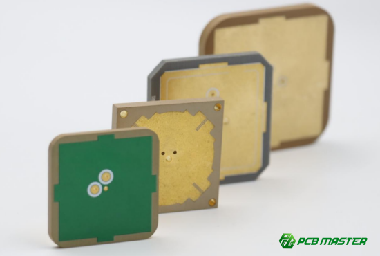
Understanding PCB Drilling: Types, Process, and How to Avoid Common Mistakes
PCB drilling is a crucial step in the manufacturing process of printed circuit boards (PCBs), directly impacting both the performance and reliability of electronic devices. Whether it’s connecting multiple layers, securing electronic components, or providing mechanical support, every hole drilled in a PCB plays a specific role. However, the seemingly simple task of drilling can present numerous challenges—from improper hole spacing to mismatched designs—that can compromise the integrity of the final product.
Understanding the types of holes, the right techniques, and the potential pitfalls is essential for ensuring high-quality, functional PCBs. This article will explore the core principles of PCB drilling, common mistakes in design and manufacturing, and best practices to avoid costly errors. By following these guidelines, you can optimize your PCB design and production, ensuring your project meets both technical requirements and industry standards.
What is PCB Drilling?
PCB drilling is the process of creating holes in a printed circuit board (PCB) to serve various functions like electrical connections and component mounting. It involves using precise drilling techniques to create holes of different sizes and shapes, tailored to the specific needs of the board design. Drilling is a critical step in the PCB manufacturing process, ensuring that all electrical connections and mechanical support structures are properly formed.
What is the Purpose of PCB Drilling?
The primary purpose of PCB drilling is to create pathways for electrical connections and to secure components onto the board. Drilled holes allow electrical signals to pass between different layers of a multi-layer PCB, enabling the device to function. Additionally, drilling is used to make holes for mounting electronic components like resistors, capacitors, and connectors. Some holes are purely mechanical, used for fixing the PCB to enclosures or for accurate positioning within the assembly.
For example, when building a mobile phone, PCB drilling connects different circuit layers and holds the tiny components in place, ensuring that the phone’s circuit functions correctly.
Why is Drilling Important in the PCB Manufacturing Process?
Drilling is crucial because it directly impacts the performance and reliability of the final product. A well-drilled PCB ensures that all electrical pathways are intact and that components are securely mounted. If holes are incorrectly sized or misaligned, the entire PCB could fail to function. Moreover, poorly drilled holes can lead to issues such as electrical shorts, signal loss, or mechanical failure.
In real-life scenarios, like the production of a car’s electronic control unit (ECU), accurate drilling ensures that the circuits work efficiently and safely within the vehicle. Inaccuracies in drilling can lead to malfunctioning or even catastrophic failures in devices, making it one of the most critical steps in PCB manufacturing.
What Are the Different Types of PCB Drilling?
The different types of PCB drilling include through-holes, component holes, mounting holes, locating holes, plated through-holes (PTH), non-plated through-holes (NPTH), and various shapes like round, slot, non-circular, blind, and back-drilled holes, each serving specific electrical or mechanical functions.
Through-Hole vs. Component Holes: Differences and Applications
Feature Through-Hole (Via) Component Hole Purpose Used to connect different layers in a multi-layer PCB Used to mount and secure electronic components like resistors and capacitors Structure Passes through the entire PCB Typically only goes through one or two layers Electrical Conductivity Allows electrical signals to pass between layers Usually has no electrical function unless specifically designed to Common Uses Multi-layer PCB connections, power and signal routing Secure components, such as LEDs or connectors, to the PCB Example Motherboards, computer circuits Simple circuit boards, basic electronics
| Feature | Through-Hole (Via) | Component Hole |
| Purpose | Used to connect different layers in a multi-layer PCB | Used to mount and secure electronic components like resistors and capacitors |
| Structure | Passes through the entire PCB | Typically only goes through one or two layers |
| Electrical Conductivity | Allows electrical signals to pass between layers | Usually has no electrical function unless specifically designed to |
| Common Uses | Multi-layer PCB connections, power and signal routing | Secure components, such as LEDs or connectors, to the PCB |
| Example | Motherboards, computer circuits | Simple circuit boards, basic electronics |
Mounting and Locating Holes: Non-Electrical Functions and Structural Uses
Feature Mounting Hole Locating Hole Purpose Secures the PCB to a case or chassis Helps position and align the PCB during assembly Electrical Function No electrical function No electrical function Size Usually larger than other hole types Often smaller for alignment purposes Common Uses Mounting PCB in enclosures or devices Aligning PCB in automated pick-and-place machines Example Desktop power supply, camera modules Mobile phone PCBs, automotive electronics
| Feature | Mounting Hole | Locating Hole |
| Purpose | Secures the PCB to a case or chassis | Helps position and align the PCB during assembly |
| Electrical Function | No electrical function | No electrical function |
| Size | Usually larger than other hole types | Often smaller for alignment purposes |
| Common Uses | Mounting PCB in enclosures or devices | Aligning PCB in automated pick-and-place machines |
| Example | Desktop power supply, camera modules | Mobile phone PCBs, automotive electronics |
Conductivity Classification: Differences Between PTH and NPTH
Feature PTH (Plated Through Hole) NPTH (Non-Plated Through Hole) Copper Plating Copper is plated inside the hole for electrical conductivity No copper plating, typically for mechanical use Electrical Function Allows electrical connection between PCB layers No electrical function, used for mechanical purposes Common Uses Multi-layer PCB connections, signal routing Mounting holes, locating holes Example Arduino boards, computer motherboards Simple PCBs, mechanical components
| Feature | PTH (Plated Through Hole) | NPTH (Non-Plated Through Hole) |
| Copper Plating | Copper is plated inside the hole for electrical conductivity | No copper plating, typically for mechanical use |
| Electrical Function | Allows electrical connection between PCB layers | No electrical function, used for mechanical purposes |
| Common Uses | Multi-layer PCB connections, signal routing | Mounting holes, locating holes |
| Example | Arduino boards, computer motherboards | Simple PCBs, mechanical components |
Hole Shapes and Design: Round, Slot, and Non-Circular Holes
Feature Round Hole Slot Hole Non-Circular Hole Shape Circular Rectangular with rounded edges Irregular, custom shapes Common Uses General through-hole and component holes Used for adjustable mounts or component placements Specialized components that require precise fitting Manufacturing Ease Easy to produce, commonly used Requires special equipment Requires custom equipment and processes Example LED mounting on PCBs Adjustable connectors in computer circuits Custom mounts in high-tech or medical devices
| Feature | Round Hole | Slot Hole | Non-Circular Hole |
| Shape | Circular | Rectangular with rounded edges | Irregular, custom shapes |
| Common Uses | General through-hole and component holes | Used for adjustable mounts or component placements | Specialized components that require precise fitting |
| Manufacturing Ease | Easy to produce, commonly used | Requires special equipment | Requires custom equipment and processes |
| Example | LED mounting on PCBs | Adjustable connectors in computer circuits | Custom mounts in high-tech or medical devices |
Blind and Back Drilled Holes: Special Hole Types and Uses
Feature Blind Hole Back Drilled Hole Depth Drilled to a specific depth, does not go through the PCB Drilled through the PCB but removes copper plating from the via Electrical Function Connects internal layers without passing through the board Reduces signal loss by removing copper plating from vias Use Case High-density PCBs with multiple layers Signal-critical applications requiring minimized signal interference Example Communication equipment PCBs High-speed data transfer PCBs, RF boards
| Feature | Blind Hole | Back Drilled Hole |
| Depth | Drilled to a specific depth, does not go through the PCB | Drilled through the PCB but removes copper plating from the via |
| Electrical Function | Connects internal layers without passing through the board | Reduces signal loss by removing copper plating from vias |
| Use Case | High-density PCBs with multiple layers | Signal-critical applications requiring minimized signal interference |
| Example | Communication equipment PCBs | High-speed data transfer PCBs, RF boards |
What Are the Key Elements of PCB Drilling?
The key elements of PCB drilling include selecting the right drill bits (such as carbide), using backing plates and cover sheets for protection, and following a precise process flow of file preparation, drilling, and inspection to ensure accuracy and quality.
Drill Bits and Material Selection: Characteristics and Use of Carbide Drill Bits
Drill Bit Material: Carbide drill bits, often made from tungsten carbide, are the most commonly used tools for PCB drilling. Tungsten carbide is extremely hard and durable, allowing it to withstand the intense pressure and heat generated during drilling. The main advantage of carbide drill bits is their ability to maintain sharpness for longer periods compared to other materials, leading to a more precise and cleaner hole. However, carbide is brittle, meaning the drill bit can break if improperly handled or used on hard materials.
Example: Carbide drill bits are ideal for drilling holes in multi-layer PCBs used in mobile phones or computers, where precision and durability are key.
Specialized vs. Standard Drill Bits: Specialized drill bits are designed for specific tasks, such as drilling small holes or handling unique PCB materials. These are more expensive and are used when high precision is required. Standard drill bits, on the other hand, are versatile and used for general-purpose drilling. They are cost-effective but may not offer the same level of precision or durability as specialized bits.
Example: A specialized drill bit might be used for drilling very fine vias in a high-density PCB, while a standard drill bit would be used for larger, less precise holes.
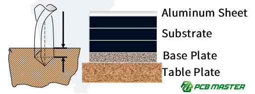
Pads and Cover Sheets: Protection and Accuracy Assurance
Pads (Backing Plates): Backing plates are placed underneath the PCB to prevent the drill bit from damaging the surface and to reduce the chance of rough edges or burrs on the drilled hole. The backing plate also helps in cleaning the drill bit by clearing the chips or debris that can accumulate during the drilling process. Using an appropriate backing plate ensures that the hole’s edges remain smooth, which is critical for component placement and soldering.
Example: In the manufacturing of automotive PCBs, using the right backing plate ensures that the tiny holes for component leads are clean and free from burrs, preventing issues during the assembly process.
Cover Sheets: Cover sheets are placed over the PCB to protect its surface from scratches or damage during the drilling process. They also guide the drill bit for precise entry into the PCB, ensuring accuracy and preventing the drill bit from slipping. The cover sheet is typically made of soft materials like aluminum foil or specialized plastic sheets.
Example: For medical device PCBs, where precision is crucial, cover sheets ensure that delicate copper traces and pads are not damaged, maintaining both the electrical and mechanical integrity of the PCB.
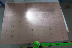
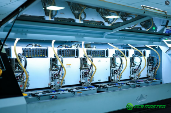
Drilling Process Flow: Standard Steps and Quality Control
File Preparation → Loading and Fixing → Drill Bit Installation → Program Loading → Drilling → Unloading and Inspection: The PCB drilling process follows a structured series of steps:
1. File Preparation: The drill file containing the design specifications is prepared. This includes the location and size of each hole.
2. Loading and Fixing: The PCB is placed and fixed onto the drilling machine, ensuring that it stays in position during the drilling process.
3. Drill Bit Installation: The correct drill bits are installed, depending on the size and type of holes required.
4. Program Loading: The drilling machine is loaded with the program that will guide the drilling process, ensuring precise hole locations.
5. Drilling: The machine drills the holes as per the design specifications.
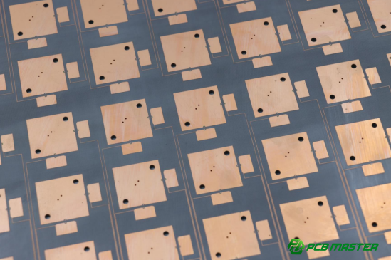
6. Unloading and Inspection: After drilling, the PCB is unloaded, and each hole is inspected for accuracy, ensuring the correct depth, diameter, and placement.
Example: In the production of a smartphone PCB, each step ensures that the tiny vias and component holes align perfectly, allowing for smooth electrical signals between the layers.
Ensuring Accuracy at Each Step: To ensure precision and avoid errors, each step in the process must be carefully controlled. For example, accurate file preparation ensures the correct hole placement, while precise drill bit installation guarantees the right size holes. The drilling machine must be calibrated properly to avoid errors during the drilling process. After drilling, automated systems or operators visually inspect the holes to ensure they meet quality standards. Regular maintenance of the drilling machine also plays a key role in maintaining consistent accuracy over time.
Example: In PCB assembly for high-speed data devices, each drilling step must be precise to prevent signal loss or interference, as even a small error can cause the device to malfunction.

What Are the Key Parameters of PCB Drilling?
The key parameters of PCB drilling include spindle speed, feed rate, retract speed, and panel stacking, which must be carefully balanced to ensure both efficient production and high-quality hole precision.
Spindle Speed and Feed Rate: How to Balance Efficiency and Quality?
Spindle Speed (RPM): Spindle speed refers to how fast the drill bit rotates. Too high of a spindle speed can cause excessive heat, potentially burning or damaging the PCB material, while too low of a speed can result in the drill bit losing efficiency, increasing the likelihood of drill bit wear, and making the drilling process less efficient. The optimal speed depends on the material being drilled and the size of the hole.
Example: In drilling FR-4 PCBs (a common PCB material), a spindle speed that's too high may cause the fiberglass to burn, while a very low speed might not cut through the layers cleanly, leading to rough edges.
Feed Rate: Feed rate is how fast the drill bit moves into the material. A faster feed rate can make the process quicker but may lead to poor hole quality, such as rough edges or burrs. A slower feed rate allows for higher precision, producing smoother hole walls but increases the drilling time. Balancing feed rate and spindle speed is essential for achieving high-quality holes while maintaining production efficiency.
Example: For smaller holes in high-precision devices, such as medical equipment PCBs, slower feed rates are preferred for smoother, burr-free holes.
Retract Speed and Panel Stacking: Key to Reducing Production Costs
Retract Speed: Retract speed refers to how quickly the drill bit withdraws after drilling through the PCB. If the retract speed is too slow, it can cause unnecessary friction, leading to wear on both the drill bit and the PCB material, especially at the hole's exit. A fast retract speed minimizes the risk of friction-related issues but must be controlled to avoid damaging the hole's edges.
Example: In automotive PCB production, a slower retract speed might cause the drill bit to create micro-tears or cause damage at the hole exit, which could affect the electrical performance of the board.
Panel Stacking (Stack-up Quantity): Stacking refers to drilling multiple PCBs at once to improve efficiency. The number of panels stacked together depends on the drill bit size and the thickness of the material. Stacking more panels allows for greater throughput but may affect precision, especially with thinner boards. The ideal stack-up number is determined by the thickness of the PCB and the smallest drill bit in use. Proper optimization of panel stacking helps balance production speed and hole quality.
Example: In consumer electronics like smartphones, increasing the number of stacked PCBs during drilling can speed up production, but it requires careful calibration to ensure that the drilling process does not compromise the accuracy of each PCB.
What Are the Common Design Errors in PCB Drilling?
Common design errors in PCB drilling include improper hole spacing, incorrect trace-to-hole distance, and misusing plated or non-plated through-holes, all of which can lead to electrical failures or manufacturing defects.
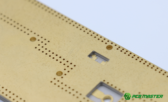
Hole Spacing Design: How Should the Distance Between Holes Be Planned?
Impact of Too-Close Hole Spacing: When holes are placed too close together, the material between them becomes weak and prone to breaking or cracking during drilling. This can lead to what is called "broken holes" or "cracked edges," which can compromise the integrity of the PCB, causing electrical or mechanical failure. The smaller the distance between holes, the higher the stress on the PCB material, making it prone to damage.
Example: In the production of high-density circuit boards, such as those in smartphones, poor hole spacing can lead to cracks or broken connections between components, resulting in board failure.
Recommended Standards and Common Mistakes: The minimum recommended hole-to-hole spacing generally depends on the PCB’s thickness and the drill size. A good rule of thumb is to ensure that the distance between holes is at least equal to the thickness of the PCB. Common design mistakes include ignoring these spacing standards, which can lead to serious manufacturing defects or functional issues in the final product.
Example: A typical mistake might be in a design for a wearable device, where engineers place holes too close together, which could cause short circuits or mechanical failures during assembly.
Distance from Traces to Holes: What Are the Potential Risks to Electrical Performance?
Risk of Short Circuits or Open Circuits: If a hole is placed too close to a PCB trace, the drill bit could damage the trace during drilling, resulting in either a short circuit (if the hole touches multiple traces) or an open circuit (if the trace is completely cut off). This can lead to faulty connections or malfunctioning circuits, severely impacting the electrical performance of the PCB.
Example: In a PCB used for power supply units, drilling too close to the power trace can lead to a short circuit, causing overheating or failure of the power components.
Proper Safety Spacing for Traces and Holes: To prevent damage to traces, it's essential to maintain a safe distance between the holes and any PCB traces. This distance is often referred to as the “trace-to-hole” clearance. The ideal clearance depends on the size of the traces and the holes, but a general recommendation is to leave at least 0.25mm between the hole edge and the trace. This ensures both electrical and mechanical reliability.
Example: For a communication device PCB, maintaining proper spacing between holes and signal traces is critical to avoid interference and signal degradation, ensuring clear communication signals.
Non-Plated Through-Hole Errors: How to Avoid Design Mistakes?
Impact of Misusing PTH and NPTH: PTH (Plated Through-Hole) and NPTH (Non-Plated Through-Hole) serve different purposes. PTH holes are electrically conductive, while NPTH holes are not. Misusing these types of holes, such as mistakenly using an NPTH where a PTH is needed, can result in connectivity issues or incorrect component mounting. For example, a hole designed to be a connection between layers could end up being non-conductive, making the PCB non-functional.
Example: In a multi-layer PCB for a wireless device, using NPTHs instead of PTHs for signal vias could cause the device to fail because the electrical connection between layers would be lost.
How to Correctly Differentiate PTH from NPTH: To avoid confusion between PTH and NPTH, designers should ensure that they are correctly specifying each hole type in the PCB’s Gerber files and drill drawings. PTHs should be clearly marked as "plated," and NPTHs should be marked as "non-plated" to prevent errors during the manufacturing process. Double-checking the design files before sending them for production can prevent such issues.
Example: In a medical device PCB, where reliability is critical, ensuring that all required vias are PTHs can prevent failure in the device’s functionality, especially for power and signal routing.
What Are the Common Manufacturing Errors and Precautions in PCB Drilling?
Common manufacturing errors in PCB drilling include drill bit wear leading to poor hole quality and incorrect parameter settings, which can result in defects like "nail heads" and "burrs," impacting the PCB’s functionality and appearance.
Drill Bit Wear: How to Prevent Drill Bit Wear from Affecting Hole Quality?
Drill Bit Lifespan Management and Replacement Cycle: Drill bits, especially those made from materials like carbide, wear down over time. Regular monitoring of the drill bit’s lifespan is crucial to ensure consistent hole quality. The replacement cycle depends on factors such as the number of holes drilled, the material being drilled, and the type of bit used. Scheduling regular checks and timely replacements will prevent performance degradation, ensuring the precision of the drilled holes.
Example: In high-volume PCB production for consumer electronics, replacing drill bits after a set number of holes or a specified time ensures that holes remain smooth and precise, avoiding issues like burrs or irregular hole sizes.
Impact of Wear and Methods to Handle It: As drill bits wear, they lose sharpness and may cause irregular hole shapes, rough edges, or even drilling errors. Worn bits can also generate more heat, which may damage the PCB material. To handle this, regular maintenance and sharpening or replacing of the drill bits are required. If a bit is worn, the PCB manufacturer can inspect the affected holes, clean up the edges, or re-drill to restore quality.
Example: In a PCB used for medical devices, worn drill bits could lead to poor hole quality, affecting the functionality of critical components, such as sensors, requiring rework and additional costs.
Incorrect Parameter Settings: How to Choose Parameters for Different Materials and Board Thicknesses?
Material-Specific Process Requirements: Different PCB materials, such as FR-4, high-frequency boards, and aluminum-based boards, require specific drilling parameters to ensure optimal results. For example, FR-4 (a common PCB material) requires moderate speed and feed rate, while high-frequency boards might need slower speeds to prevent signal distortion. Aluminum PCBs, due to their metal base, require different speeds and cooling methods to avoid warping or damaging the material.
Example: When drilling high-frequency PCBs used in communication devices, using the correct speed and feed rate ensures that the holes maintain the required precision without affecting the board’s signal integrity.
Incorrect Settings Leading to "Nail Head" and "Burr" Issues: If drilling parameters (such as speed, feed rate, and retract speed) are incorrectly set, it can result in common defects like "nail heads" (excess material around the hole) and "burrs" (sharp protrusions at the hole's edge). These defects not only impact the aesthetic quality of the PCB but can also affect component placement and soldering, leading to long-term functional issues.
Example: In the production of a PCB for a power supply unit, using a high feed rate or low spindle speed may cause burrs around holes, making it difficult to mount components securely and increasing the risk of soldering failures.
What Are the Key Design and Processing Considerations for Special Hole Types?
Key design and processing considerations for special hole types, such as blind and buried holes, include precise depth control to avoid drilling errors and the challenges of ensuring accurate alignment and depth in multi-layer PCBs for reliable connections.
Blind and Buried Holes: Precision Requirements for Depth Control
How to Avoid Drilling Too Deep or Too Shallow: Both blind and buried holes require precise depth control, as drilling too deep can damage other layers or cause the hole to extend where it is not needed. Drilling too shallow can result in incomplete connections between layers, causing poor electrical or mechanical performance. To avoid these issues, it is essential to use precise drilling equipment with depth control features, such as laser depth measurement or multi-step drilling processes. Regular calibration and proper programming of drilling machines ensure that the correct depth is achieved consistently.
Example: In multi-layer PCB designs used for smartphones, a drilled blind hole that is too deep may interfere with internal components, while a hole that is too shallow can result in weak electrical connections between layers, leading to device malfunctions.
Blind and Buried Holes in Multi-Layer Boards: Applications and Challenges: Blind and buried holes are often used in multi-layer PCBs to connect different layers or create specific paths without passing through the entire board. Blind holes connect external layers to internal layers, while buried holes only connect internal layers. These types of holes are particularly important in high-density designs, like those used in telecommunications or high-performance computing. However, drilling these holes is challenging because it requires precise alignment and depth control to avoid damaging other layers or creating defects in the board. The use of advanced drilling techniques and specialized machines can help ensure the quality of these holes.
Example: In high-performance PCB designs for networking equipment, blind and buried holes are essential for routing signals between different layers, but the process requires extreme accuracy to ensure the board’s reliability and prevent signal interference.
Conclusion
Understanding the complexities of PCB drilling, from hole types to parameter settings, is essential for ensuring high-quality, reliable circuit boards. Whether it's optimizing drill bit wear, managing hole spacing, or mastering specialized hole designs, precision at every step of the manufacturing process is crucial. This level of expertise requires not only technical knowledge but also reliable partners who can deliver consistently superior results.
As an experienced PCB and PCBA supplier, PCBMASTER is committed to providing top-tier products that meet the highest industry standards. With years of expertise in PCB manufacturing, we ensure that each board is crafted to perfection, offering the best in quality, performance, and reliability for a variety of applications. Partner with PCBMASTER to experience precision and excellence in every layer.
FAQs
1. Why Should Hole Spacing Be Avoided Too Close Together?
When holes are spaced too closely, the material between them becomes weakened, which increases the risk of the PCB material cracking or breaking during the drilling process. This can lead to issues like "broken holes" or "cracked walls," compromising the PCB's structural integrity. These defects not only affect the mechanical reliability of the board but also its long-term performance, potentially shortening its lifespan. Ensuring proper hole spacing is essential to prevent such damage and to maintain the overall reliability and durability of the PCB in its final application.
2. How to Avoid Mismatches Between Drill Files and Gerber Files?
To prevent mismatches between drill files and Gerber files, it's important to perform a layered overlay check using specialized software. This check helps to verify that each hole in the drill file corresponds to a pad in the Gerber file. Additionally, ensure that the pad sizes are appropriate for the drill holes, as mismatched sizes can cause issues during manufacturing. By overlaying the files and checking the alignment, manufacturers can identify any discrepancies before production begins, minimizing the risk of defects or misalignments in the final PCB.
3. How to Choose Appropriate Drilling Parameters?
Drilling parameters should be selected based on the type of PCB material and its thickness. For instance, materials like FR-4, high-frequency boards, or aluminum-based boards all have different drilling requirements. A high spindle speed or fast feed rate may cause issues like rough hole walls or even damage the drill bit, while too low a speed can lead to inefficient drilling and excess wear. The ideal drilling parameters should be carefully adjusted to suit the material properties, ensuring smooth hole walls, efficient production, and optimal tool longevity. Regular adjustments to these settings are crucial for maintaining high-quality drilling.
4. What Is the Difference Between Blind and Buried Holes, and How to Design Them?
Blind holes are holes that connect to only one layer of the PCB, while buried holes are entirely enclosed within the inner layers and do not pass through to the surface. When designing these holes, it is critical to control the depth accurately. Blind holes must not exceed the layer they are meant to connect to, while buried holes should only go through the intended inner layers without breaking into the outer layers. Proper depth control and alignment during drilling are essential to ensure the holes serve their intended purpose without damaging other layers or compromising the electrical connection between layers.
5. How Does Drill Bit Wear Affect Hole Quality?
As drill bits wear over time, they lose sharpness, leading to smaller hole diameters, rougher hole walls, or the formation of burrs (small, unwanted protrusions around the hole). These issues negatively impact the electrical performance of the PCB and make component assembly more difficult. Worn drill bits also increase the risk of damage to the PCB material, leading to further defects. To avoid these problems, drill bits should be regularly inspected and replaced based on the manufacturer’s recommended replacement cycle, ensuring that each hole remains within the required specifications for optimal PCB performance and assembly precision.
Author Bio
Hi, I'm Carol, the Overseas Marketing Manager at PCBMASTER, where I focus on expanding international markets and researching PCB and PCBA solutions. Since 2020, I've been deeply involved in helping our company collaborate with global clients, addressing their technical and production needs in the PCB and PCBA sectors. Over these years, I've gained extensive experience and developed a deeper understanding of industry trends, challenges, and technological innovations.
Outside of work, I'm passionate about writing and enjoy sharing industry insights, market developments, and practical tips through my blog. I hope my posts can help you better understand the PCB and PCBA industries and maybe even offer some valuable takeaways. Of course, if you have any thoughts or questions, feel free to leave a comment below—I'd love to hear from you and discuss further!

