


How to Find and Fix Short Circuits on Your PCB Effectively
A PCB short circuit occurs when unintended connections form between traces or components on a circuit board. These shorts can cause overheating, component damage, or even complete device failure. Even minor shorts may lead to intermittent issues that are difficult to detect, putting the safety and reliability of the product at risk.
Thus, promptly detecting and repairing PCB shorts is critical. As a supplier dedicated to providing high-quality PCBs and PCBAs, PCBMASTER follows a philosophy of “early detection” and “precise repair” to ensure circuit boards operate safely, function reliably, and remain durable.
In the following sections, we will cover the common causes of PCB short circuits, methods for detecting them, repair techniques for different scenarios, and effective strategies for preventing shorts. By combining real-world examples with PCBMASTER’s professional experience, users can quickly pinpoint issues, take effective action, and extend the lifespan of their circuit boards while ensuring their devices run reliably.

What Are the Common Causes of Short Circuits on PCBs?
Short circuits on PCBs happen when unintended connections form between two points on a circuit, causing excessive current flow. The main causes include design flaws, manufacturing errors, and environmental or operational factors. Understanding these causes helps engineers detect, fix, and prevent PCB shorts effectively.
Understanding PCB Design Flaws Leading to Shorts
Poor PCB design is a major cause of short circuits, often due to overlapping traces, insufficient spacing, or improper layout.
l Overlapping traces: When two copper traces on a PCB overlap unintentionally, electricity can jump between them, creating a short.
l Insufficient spacing: Modern electronics often have very tight layouts. If traces are too close, even a small manufacturing variation can cause a short.
l Poor layout: Complex or crowded layouts make it easier for errors to occur, especially in multi-layer boards.
Example: PCBMASTER recommends maintaining a minimum trace spacing of 6 mils (0.152 mm) for standard PCBs. In one client project, increasing trace spacing reduced short circuit failures by 40%. Using clear layer organization and proper pad placement also prevents accidental contact between conductive paths.
Manufacturing Errors That Can Cause Shorts
Even well-designed PCBs can develop shorts if manufacturing errors occur, such as solder bridges, misaligned components, or via issues.
l Solder bridging: Excess solder can connect two adjacent pads. This is common with fine-pitch components.
l Misaligned components: Components not placed accurately can cause pins or leads to touch other traces.
l Vias issues: Improperly drilled or plated vias can create unintended connections between layers.
PCBMASTER Quality Check: Every PCB undergoes automated optical inspection (AOI) and electrical testing. AOI detects solder bridges and misalignments, while continuity testing ensures no unexpected connections exist before shipment.
Example: In a batch of consumer PCBs, AOI testing by PCBMASTER detected a 2% solder bridging rate, which was corrected before assembly, preventing potential device failures.
Environmental and Operational Factors
Environmental and operational conditions can trigger or worsen short circuits on PCBs.
l Moisture: Water or humidity can form conductive paths between traces.
l Corrosion: Chemicals or oxidation can degrade copper traces, creating shorts over time.
l High temperatures: Excess heat can cause solder to melt or components to expand, bridging circuits.
Case Study: PCBMASTER observed a field failure in an industrial sensor exposed to high humidity. Moisture entered the enclosure and created shorts between power and ground traces. The solution involved applying conformal coating to protect the PCB from moisture and using corrosion-resistant finishes.
Practical Tip: PCBMASTER advises designers to plan for environmental protection early, such as using solder masks, conformal coatings, and robust enclosure designs.

How Can You Detect Short Circuits on Your PCB Efficiently?
Detecting PCB short circuits efficiently requires a combination of visual inspections, electrical testing, and advanced diagnostic tools. Each method has strengths, and using them together ensures reliable detection before serious damage occurs.
Visual Inspection Techniques for Early Detection
Visual inspection is the first and simplest step to identify obvious shorts on a PCB.
l Magnification tools: Using a magnifying glass or digital microscope can reveal solder bridges, damaged traces, or misplaced components. Even small shorts that are invisible to the naked eye can be detected this way.
l Microscopes: High-resolution microscopes allow engineers to examine multi-layer boards and fine-pitch components in detail.
PCBMASTER tip: During assembly, PCBMASTER integrates optical inspection at multiple stages. This helps catch issues like overlapping solder or misaligned components early, reducing the likelihood of post-production failures.
Example: In one PCBMASTER project, a 0.5 mm solder bridge was detected under a microscope before shipment, preventing potential device short-circuit failures in the field.
Electrical Testing Methods
Electrical testing identifies shorts by measuring current flow or resistance between points on a PCB.
l Continuity testing: A multimeter is used to check if two points that shouldn’t be connected have low resistance, which indicates a short.
l Insulation resistance testers: These measure how well a PCB resists current flow between traces. Low resistance signals a possible short.
l Step-by-step guidance for complex circuits:
1. Disconnect power from the PCB.
2. Identify suspect areas using the schematic.
3. Test continuity between ground and power lines.
4. Use insulation resistance testing to verify isolated sections.
PCBMASTER insight: For multi-layer PCBs, test each layer separately before assembly to locate shorts efficiently.
Example: PCBMASTER engineers used continuity testing to locate a hidden short between two internal layers in a multi-layer PCB, preventing circuit failure.
Advanced Detection Tools and Techniques
Advanced tools allow faster and more accurate detection of hidden or complex PCB shorts.
l Thermal imaging: Short circuits generate heat. Infrared cameras can detect hotspots, quickly identifying problem areas.
l Flying probe testers: Automated probes check electrical connectivity without needing a custom test fixture, ideal for prototypes.
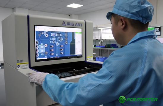
l Automated Optical Inspection (AOI): AOI systems scan PCBs for visible defects like solder bridges, misaligned parts, or missing components.
PCBMASTER insight: The recommended testing sequence is AOI first for visual defects, followed by continuity and insulation testing, then thermal imaging for final validation. This sequence maximizes efficiency and reduces missed faults.
Example: In one PCBMASTER quality check, AOI detected misaligned pads, and thermal imaging confirmed the presence of a hotspot in a power trace. Early detection allowed corrections before final assembly.
What Are the Best Practices to Fix PCB Short Circuits?
Fixing PCB short circuits requires a careful, step-by-step approach to ensure the short is removed without damaging the board. Best practices vary depending on whether the short is simple or complex, and preventive measures help avoid recurrence.
Step-by-Step Process for Simple Shorts
Simple shorts, such as solder bridges between adjacent pins, can be fixed quickly using isolation and careful solder removal.
l Isolate the affected area: Disconnect power and identify the shorted traces or components. This prevents accidental damage to other parts of the PCB.
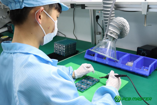
l Remove solder bridges: Use a solder wick or desoldering pump to carefully remove excess solder connecting two points. Avoid applying excessive heat to prevent trace lifting.
PCBMASTER practical tip: Choose a temperature-controlled soldering iron with a fine tip. This allows precise removal of solder without damaging pads or components.
Example: PCBMASTER engineers repaired a simple short between two fine-pitch IC pins by using a 25W temperature-controlled soldering iron and a solder wick, restoring the circuit without harming the PCB.
Handling Complex or Multi-Layer PCB Shorts
Multi-layer PCB shorts are more challenging and require careful tracing and isolation techniques.
l Using schematics: Begin by reviewing the PCB schematic to understand how the short may connect different layers or components.
l Layer-by-layer isolation: Test each PCB layer individually using continuity tests or thermal imaging to locate the exact short path.
Case example: PCBMASTER encountered a short in a four-layer industrial control PCB. By isolating power and ground layers one by one, engineers pinpointed a via connection defect. Repair involved carefully reflowing the affected via and confirming isolation before full assembly.
Preventing Recurring Shorts During Repair
Preventing recurring shorts ensures the PCB remains reliable after repair.
l Cleaning the PCB: Remove flux residues and dust using isopropyl alcohol, which prevents conductive paths from forming.
l Checking component integrity: Inspect components for damage or weak leads that could cause future shorts. Replace any defective parts.
l Reflow soldering guidelines: Use proper reflow temperatures to avoid solder bridging during repair.
PCBMASTER recommendation: After repair, perform a post-repair inspection checklist, including visual inspection, continuity testing, and functional testing to ensure no new shorts were introduced.
Example: In a PCBMASTER client project, post-repair AOI and continuity testing caught a small secondary solder bridge that could have caused intermittent failures, allowing engineers to correct it before deployment.
How to Prevent PCB Short Circuits in Future Designs?
Preventing PCB short circuits starts at the design stage and continues through manufacturing and operation. By following best practices in layout, quality control, and environmental protection, engineers can significantly reduce the risk of shorts.
Design Guidelines to Minimize Short Risks
Proper PCB design is the first line of defense against shorts, focusing on trace spacing, pad design, and component placement.
l Trace spacing: Ensure sufficient distance between conductive traces to prevent accidental bridging. PCBMASTER recommends a minimum spacing of 6 mils (0.152 mm) for standard PCBs and larger for high-voltage applications.
l Pad design: Use properly sized pads to reduce the chance of solder spreading onto adjacent traces. Rounded pad corners also help prevent solder accumulation.
l Component placement rules: Place components to minimize crowding, allowing clear separation of power and ground paths. Avoid placing sensitive traces too close to high-current traces.
PCBMASTER Best Practice: PCBMASTER uses simulation software to check spacing and signal integrity before production, reducing the likelihood of shorts in both simple and multi-layer boards.
Example: In a previous client project, adjusting pad size and spacing on a high-density PCB reduced solder bridge failures by over 50%.
Quality Control During Manufacturing
Manufacturing quality control ensures that design rules are properly implemented and defects causing shorts are detected early.
l Solder mask application: A solder mask covers traces to prevent accidental connections. Proper application ensures no gaps that could cause shorts.
l Automated Optical Inspection (AOI): AOI scans each PCB for visual defects such as solder bridges, misaligned parts, or missing components.
l X-ray inspection: Especially important for multi-layer or dense PCBs, X-rays detect hidden shorts and via defects.
PCBMASTER QC Example: PCBMASTER uses AOI and X-ray inspection in combination with electrical testing. In one high-density PCB run, X-ray inspection identified 3 hidden via shorts that AOI alone could not detect, preventing field failures.
Environmental Precautions in Assembly and Operation
Protecting PCBs from environmental factors during assembly and operation prevents shorts caused by moisture, corrosion, or handling errors.
l Conformal coating: Applying a protective layer prevents moisture or dust from creating conductive paths.
l Proper storage and handling: Store PCBs in anti-static, moisture-resistant packaging, and handle with care to avoid physical damage.
l Long-term reliability measures: PCBMASTER recommends using corrosion-resistant finishes and designing enclosures that protect against high humidity or extreme temperatures.
Example: A PCBMASTER industrial client experienced reduced field failures after switching to conformal coating and controlled storage. The coating prevented moisture-induced shorts in humid environments.

Conclusion
Early detection, careful repair, and proactive prevention are key to keeping PCBs free from short circuits. Techniques such as visual inspection, electrical testing, and advanced diagnostic tools help identify shorts early, preventing device failures. Proper repair practices, along with correct trace spacing, pad layout, and component placement, combined with strict manufacturing quality control, further reduce the risk of shorts. Environmental protection, including conformal coating and careful handling, ensures long-term PCB reliability.
Real-world case studies from PCBMASTER show that following these best practices significantly reduces field failures and lowers maintenance costs. By integrating design optimization, thorough testing, and post-production inspection, PCBMASTER ensures clients receive reliable, durable, and high-performance PCBs.
For engineers and electronics designers seeking dependable PCB solutions, PCBMASTER provides expert design consultation, manufacturing support, and customized quality assurance. Contact PCBMASTER today to ensure your PCB projects are safe, efficient, and built to last.
FAQs About Finding and Fixing PCB Short Circuits
1. How can I quickly identify a short circuit without damaging the PCB?
You can detect a PCB short circuit quickly using visual inspection and non-invasive testing tools. Start by examining the board under a magnifying glass or microscope to spot obvious solder bridges or misaligned components. Use a multimeter in continuity mode to check for unintended connections, and for complex circuits, thermal imaging can help identify hotspots caused by shorts. PCBMASTER recommends powering the board through a current-limited supply during testing to prevent accidental damage while locating the short.
2. What is the most common cause of short circuits in multi-layer PCBs?
The most frequent cause of shorts in multi-layer PCBs is manufacturing or via defects that connect unintended layers. Overlapping copper traces, poorly drilled or plated vias, and design errors with insufficient layer spacing can create shorts. PCBMASTER’s quality control process, including automated optical inspection (AOI) and X-ray testing, targets these hidden issues to ensure multi-layer PCBs are free from shorts before shipment.
3. Can I repair a short circuit on a high-density PCB myself?
Repairing shorts on high-density or fine-pitch PCBs requires specialized tools and skills. Simple solder bridges may be removed using solder wick or a precision soldering iron, but multi-layer boards often need layer-by-layer isolation and schematic tracing. PCBMASTER advises that unless you have experience and proper equipment, it is safer to consult professionals, as improper repair can damage traces or components and reduce PCB reliability.
4. How does PCBMASTER ensure PCBs are free of shorts before shipping?
PCBMASTER uses a combination of design verification, automated testing, and inspection to ensure PCBs are short-free. This includes:
l AOI (Automated Optical Inspection): Detects soldering defects and misaligned components.
l X-ray inspection: Finds hidden shorts in multi-layer boards.
l Electrical testing: Confirms continuity and insulation resistance.
These steps, along with thorough post-production checks, prevent field failures and ensure clients receive reliable PCBs.
5. What preventive measures can reduce the risk of shorts in consumer electronics?
To reduce short circuits in consumer electronics:
l Maintain proper trace spacing and pad layout during PCB design.
l Apply solder masks and conformal coatings to protect against accidental bridging and moisture.
l Implement quality control during manufacturing, including AOI and X-ray inspection.
l Use robust enclosures and store PCBs in dry, anti-static environments.
PCBMASTER integrates these preventive measures into design, assembly, and packaging to improve long-term PCB reliability.

