


Flexible PCB Assembly: Key Challenges and PCBMASTER’s Flawless Approach
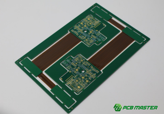
Flexible PCBs are thin, bendable circuit boards that can twist and fold to fit into small or unusual spaces. They are widely used in smartphones, wearables, medical devices, and automotive electronics because of their lightweight and space-saving design.
Correct assembly is essential for reliable performance. Flexible PCBs are delicate, and mistakes in handling, soldering, or testing can cause signal failure, short circuits, or mechanical damage. Proper control of stress points, precise component placement, and careful quality checks are critical to prevent early failures.
PCBMASTER brings years of experience in flexible PCB assembly. By using advanced processes, skilled technicians, and thorough testing, PCBMASTER handles delicate materials, maintains signal integrity, and ensures stress-resistant assembly. The following sections detail the main challenges of flexible PCB assembly and how PCBMASTER delivers flawless solutions.
How Does PCBMASTER Overcome the Key Challenges in Flexible PCB Assembly?
Challenge 1 – Handling Delicate Materials
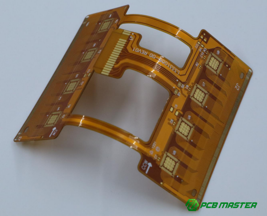
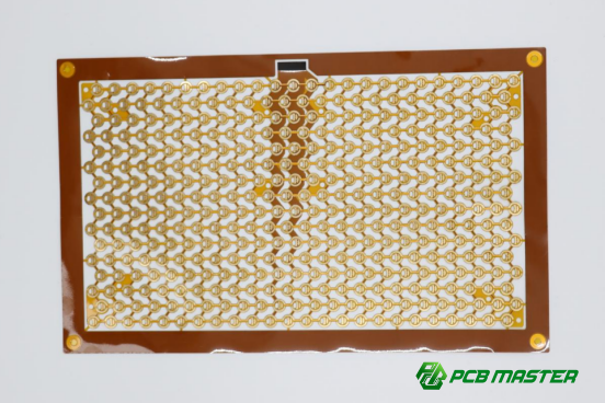
Flexible PCBs are very thin and fragile. They can tear easily, warp, or bend in unintended ways during assembly. Even small mistakes in handling can damage the board, affect connections, or ruin delicate circuits. Single-layer flexible PCBs are especially prone to tearing, while multi-layer boards can delaminate if layers are misaligned. Proper handling is one of the most critical steps in flexible PCB assembly.
Solution: Advanced Material Handling Techniques
PCBMASTER overcomes this challenge by combining specialized equipment with trained personnel. Workers are trained to handle flexible boards gently, using anti-static tools, soft fixtures, and controlled movements. Automated handling systems help reduce human error, especially for delicate multi-layer boards.
Layer alignment is another key factor. For single-layer flexible PCBs, PCBMASTER ensures that traces and components are positioned accurately before soldering. Multi-layer flexible boards require precise stacking of multiple layers without shifting, which is achieved using alignment pins and controlled pressure during lamination.
For example, in a wearable device project, PCBMASTER successfully assembled a three-layer flexible PCB with tight tolerances. Using alignment fixtures and careful manual inspection, the board was completed without tears, warping, or layer misalignment, ensuring reliable signal connections.
By applying these advanced material handling techniques, PCBMASTER minimizes the risk of damage, improves assembly yield, and guarantees that flexible PCBs maintain their integrity during production.
Challenge 2 – Maintaining Signal Integrity in Complex Designs
Maintaining signal integrity in flexible PCBs is essential because bending, folding, or dynamic movement can disrupt electrical signals. Without proper design, traces may experience crosstalk, impedance mismatch, or signal loss, leading to malfunctioning circuits. High-speed circuits and dense layouts are particularly sensitive to these problems.
Solution: Optimized Design for Manufacturability (DFM)
PCBMASTER addresses this challenge through early-stage Design for Manufacturability (DFM) optimization. Before assembly, engineers analyze the circuit layout, layer stack-up, and routing paths to minimize signal interference. Adjustments such as controlled trace widths, proper spacing between signal lines, and careful placement of ground planes help prevent crosstalk and impedance mismatches.
For example, in a wearable sensor project, PCBMASTER used a four-layer flexible PCB with high-speed data lines. By carefully routing the differential pairs and maintaining consistent trace impedance, the team prevented signal distortion even when the board was bent repeatedly.
Steps include:
1. Reviewing high-speed signal paths for potential interference.
2. Adjusting layer stacking to separate critical signals from noisy traces.
3. Optimizing trace widths and spacing to match impedance requirements.
4. Verifying signal performance through simulation and testing.
By applying DFM principles, PCBMASTER ensures that flexible PCBs maintain reliable electrical performance under bending or movement, improving long-term functionality in complex applications.
Challenge 3 – Component Placement and Soldering on Flexible Substrates
Placing components on flexible PCBs is more difficult than on rigid boards. Flexible substrates can bend or move during assembly, making it easy to misalign components. Additionally, excessive heat during soldering can damage the delicate board or create weak solder joints, known as cold soldering. Both issues can compromise the reliability of the final product.
Solution: Precision Soldering and Component Placement
PCBMASTER solves this challenge using customized soldering profiles, specialized fixtures, and selective soldering techniques. The assembly process is carefully controlled to prevent heat damage while ensuring accurate placement. Fixtures hold the flexible PCB flat and stable, allowing precise component alignment.
For example, surface-mount technology (SMT) components on a flexible board are placed using automated pick-and-place machines with controlled pressure, followed by reflow soldering using a customized thermal profile. In contrast, through-hole components require selective soldering with localized heating to avoid bending or warping the substrate.
Steps include:
1. Securing the flexible PCB with specialized fixtures.
2. Using customized heat curves for soldering to prevent substrate damage.
3. Applying automated or selective placement for accurate component alignment.
4. Inspecting solder joints to ensure proper connection and reliability.
By combining precise soldering with careful component placement, PCBMASTER ensures flexible PCBs function correctly, even under repeated bending or mechanical stress.
Challenge 4 – Mechanical Stress and Flexibility Management
Flexible PCBs often need to bend, fold, or move during use. These actions can concentrate stress on certain areas of the board, leading to cracks, broken traces, or component failure. Without proper management, mechanical stress can reduce the lifespan of the PCB and cause product malfunctions.
Solution: Stress-Resistant Assembly Practices
PCBMASTER manages mechanical stress through careful design and assembly techniques. Reinforcement methods, such as adding stiffeners or support frames, protect vulnerable areas and distribute stress evenly. Folded sections are tested for repeated bending to ensure durability. Fixtures hold the PCB securely during assembly, preventing unintended deformation.
For example, in a foldable wearable device, PCBMASTER applied stiffeners to hinge areas and conducted bend tests simulating daily use. By doing so, the PCB maintained full functionality after thousands of bending cycles without cracks or broken traces.
Steps include:
1. Identifying high-stress areas in the flexible PCB design.
2. Applying reinforcements like stiffeners or support frames.
3. Conducting fold and bend tests under simulated real-life conditions.
4. Inspecting the board for mechanical integrity before final assembly.
Through these stress-resistant assembly practices, PCBMASTER ensures flexible PCBs remain reliable even in dynamic applications, improving product longevity and performance.
Challenge 5 – Quality Assurance and Testing Limitations
Flexible PCBs are harder to inspect and test than rigid boards. Their thin, bendable materials make automated optical inspection (AOI) and other testing methods more challenging. During testing, mechanical stress can also damage the board, causing micro-cracks or early failure that may not be visible initially. Ensuring high-quality flexible PCBs requires specialized approaches.
Solution: Comprehensive Quality Control and Testing
PCBMASTER uses a combination of AOI, X-ray inspection, functional testing, and stress simulation to ensure flexible PCB reliability. AOI helps detect surface defects like misaligned components or solder issues, while X-ray inspection checks internal layers for hidden flaws such as misaligned traces or vias. Functional testing verifies that the PCB performs correctly under electrical load, and stress simulations replicate bending or folding conditions to identify potential weak points.
For example, in a medical wearable project, PCBMASTER detected micro-cracks in high-stress areas through X-ray and stress testing. Early identification allowed adjustment in assembly methods, preventing device failure during real-world use.
Steps include:
1. Performing AOI to catch surface defects.
2. Using X-ray inspection to check internal layers.
3. Conducting functional tests under real operating conditions.
4. Running stress simulations to detect early mechanical or electrical failures.
Through comprehensive quality control, PCBMASTER ensures that flexible PCBs are reliable, safe, and able to perform consistently even in demanding applications.
Challenge 6 – Continuous Improvement and Process Feedback
Even with careful handling and assembly, small defects or efficiency issues can occur during flexible PCB production. These may include minor misalignments, inconsistent soldering, or slow assembly steps. Left unaddressed, these issues can affect product quality and increase production costs. Continuous monitoring and process improvement are essential to maintain high standards.
Solution: Continuous Process Optimization
PCBMASTER addresses this challenge through defect tracking, process analysis, and ongoing improvement. Every assembly batch is reviewed for errors, and data is collected on defect types, frequency, and causes. Engineers analyze this information to adjust workflows, improve assembly techniques, and optimize equipment settings. This feedback loop ensures each new project benefits from lessons learned in previous ones.
For example, during a high-volume wearable PCB project, PCBMASTER noticed slight misalignment in SMT components due to fixture placement. By refining the fixture design and adjusting the pick-and-place settings, misalignment was eliminated in subsequent batches. This process not only improved quality but also increased production efficiency.
Steps include:
1. Monitoring defects and collecting detailed production data.
2. Analyzing root causes of defects or inefficiencies.
3. Adjusting assembly processes, equipment, and operator training.
4. Implementing improvements and tracking results in future projects.
By continuously optimizing assembly processes, PCBMASTER ensures higher reliability, reduced defects, and greater efficiency in flexible PCB manufacturing.
Conclusion
Flexible PCB assembly presents several challenges, including handling delicate materials, maintaining signal integrity, precise component placement, managing mechanical stress, ensuring thorough quality control, and continuously improving processes. PCBMASTER addresses each of these challenges with advanced techniques, such as specialized material handling, DFM optimization, precision soldering, stress-resistant assembly practices, comprehensive testing, and continuous process feedback. These solutions ensure that flexible PCBs are reliable, durable, and perform optimally in even the most demanding applications.
By combining experience, technology, and rigorous quality control, PCBMASTER delivers flexible PCBs that meet high standards for performance and longevity. Clients can trust that each board is assembled with care, tested thoroughly, and optimized for real-world use, giving confidence in product reliability and consistent performance.
For businesses and designers seeking expert flexible PCB assembly, PCBMASTER offers professional services backed by proven methods and years of experience. Contact PCBMASTER today to ensure your flexible PCB projects are assembled flawlessly, with maximum reliability and efficiency.
FAQs
What Types of Flexible PCBs Are Most Challenging to Assemble?
The most challenging flexible PCBs to assemble are multi-layer boards, high-density designs, and dynamic applications that require frequent bending or movement. Multi-layer boards need precise layer alignment, while high-density boards have closely spaced traces and components that increase the risk of short circuits. Dynamic flex PCBs must withstand repeated bending without breaking traces or components, making careful handling and stress management essential.
Can Flexible PCBs Withstand Continuous Bending?
Flexible PCBs can tolerate bending to some extent, but their durability depends on material properties, thickness, and design. Excessive or repeated bending without reinforcement can cause cracks, broken traces, or delamination. Designers often control the bend radius, add stiffeners, and select flexible materials that endure repeated motion to ensure reliability in continuous-bending applications.
How Does PCBMASTER Reduce Defects in Flexible PCB Assembly?
PCBMASTER minimizes defects by combining careful material handling, stress management, and rigorous quality assurance processes. Delicate boards are stabilized during assembly, mechanical stress is controlled with reinforcement techniques, and defects are detected through automated inspection, X-ray, functional testing, and stress simulations. These measures ensure high yield, reliability, and performance in flexible PCB assemblies.
Is It Possible to Fully Automate Flexible PCB Assembly?
Full automation in flexible PCB assembly is limited due to the board’s delicate and bendable nature. While machines can handle certain steps like pick-and-place and soldering, human operators are crucial for inspection, alignment, and handling dynamic flex sections. A combination of automation and skilled technicians provides the most reliable assembly results.
What Makes PCBMASTER’s Approach Unique?
PCBMASTER’s approach is unique because it combines extensive experience, advanced technology, and strict process control. The team applies specialized equipment, customized assembly techniques, and continuous process optimization. This integrated method ensures that flexible PCBs are assembled with precision, reliability, and high performance, even for the most complex designs.

