


How Positive and Negative Films Impact PCB Design and Production
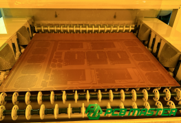
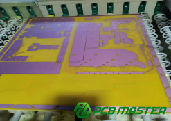
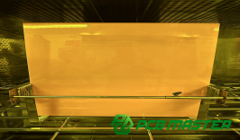
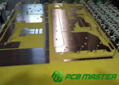
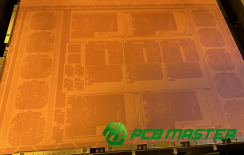
The photolithography stage in PCB (Printed Circuit Board) manufacturing is where intricate designs begin to take shape, transferring copper traces and pads onto the copper-clad board. At this crucial point, positive or negative films are used to define which areas of copper will remain and which will be etched away. These films serve as masks, guiding the creation of precise features on the board. Understanding the differences between positive and negative films is key to ensuring accuracy and efficiency in PCB production.
What are Positive and Negative Films in PCB Design?
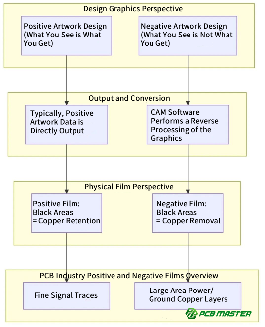
Positive and negative films in PCB design are masks used in the photolithography process, where positive film keeps copper in the black areas and removes it in the transparent areas, while negative film does the opposite, keeping copper in the transparent areas and removing it in the black areas.
What are the definitions of positive and negative films?
In PCB design, positive and negative films refer to the two types of masks used during the photolithography process to define the copper features on the board.
Positive film: In positive film, the areas that are black or opaque will remain as copper on the PCB after etching. The transparent areas will be etched away, leaving behind the copper features.
Negative film: In contrast, negative film works oppositely. The black or opaque areas on the film represent the areas that will be etched away, while the transparent areas correspond to the copper features that will remain on the PCB.
In PCB design files (like Gerber files), positive film is used to create features that will be kept on the board (such as copper traces and pads), while negative film is used to define the areas where copper should be removed.
By understanding these films, designers can control exactly where copper will remain or be removed, ensuring that the PCB performs as expected.
What are the visual differences between positive and negative films?
The main difference between positive and negative films is how the design is represented visually:
Positive film shows the design in a direct way, where the opaque (black) parts on the film correspond to the copper areas that will remain. The transparent parts will be etched away.
Example: A copper trace or pad in a positive film will appear as a solid black line or shape, which means that area will stay as copper on the PCB. The rest of the board (transparent areas) will be etched off.
Negative film, on the other hand, shows the design in reverse. The black or opaque parts represent areas where copper will be removed, and the transparent parts show where copper will stay.
Example: A copper pad in a negative film will appear as an empty space surrounded by black (indicating where the copper should be removed), leaving the copper to form around the clear area.
The choice between using positive or negative film depends on the type of features needed and the manufacturing process. For example, positive film is usually more intuitive and easier for designers to visualize, whereas negative film is often used for areas like power and ground planes.
How do these film types affect PCB design?
Positive film is typically used for signal layers and fine features, where precise copper areas are required.
Negative film is often used for power planes or ground planes, where large areas of copper are needed, and only specific sections (such as vias or isolation zones) need to be removed.
Understanding the difference between positive and negative films ensures that designers can use the right technique for each part of their PCB, ensuring the final product works efficiently and meets the design specifications.
Applications of Positive and Negative Films in PCB Design
Positive film is used in PCB design for signal layers to accurately define copper traces, while negative film is applied to power and ground planes to efficiently create large copper areas and remove unwanted regions.
What are the applications of positive film in PCB design?
Positive film is primarily used for signal layers in PCB design. These layers carry the electrical signals between components, and the precise layout of copper traces is crucial for their functionality.
Why is positive film used for signal layers?
Signal layers require high precision to ensure reliable electrical connections. Positive film offers a clear and straightforward way to represent copper traces: the black parts on the film correspond to the copper that will remain, while the transparent parts will be etched away. This makes it easier to visualize and check the connections between components, especially in complex designs.
How do designers use positive film for checking connections?
Designers can easily inspect the layout by looking at the positive film. Since the traces are directly represented in black (opaque), it’s clear where the copper will remain. This allows engineers to quickly identify potential errors or missing connections, ensuring that all circuits are properly designed before moving forward with the manufacturing process.
In summary, positive film is used in signal layers because it provides an intuitive and precise way to ensure the correct copper traces and electrical connections. It is especially helpful for quick visual checks and troubleshooting during the design phase.
What are the applications of negative film in PCB design?
Negative film is commonly used for designing power planes and ground planes in PCB layouts, where large areas of copper are needed.
Why is negative film used for power and ground planes?
In power and ground planes, large, uninterrupted copper areas are necessary to provide stable power distribution across the PCB. Negative film is ideal because it allows designers to easily "cut out" regions where copper is not needed, such as around vias or in areas that need isolation. The film is used to block out areas where copper should not be, leaving the rest to be etched away, forming large copper planes.
How does negative film improve design efficiency?
Using negative film for power and ground planes is efficient because it reduces the complexity of the design. Instead of manually drawing each copper feature, designers can use negative film to quickly define large areas where copper should remain. The areas that need to be removed (like around vias, holes, or isolation zones) are simply left transparent. This speeds up the design process and reduces the chance of errors.
In short, negative film is used for power and ground planes because it simplifies the creation of large copper areas while allowing designers to easily define and remove unwanted copper regions. This approach increases design efficiency and reduces the time needed to finalize the PCB layout.
Differences and Applications of Positive and Negative Films in PCB Design
Positive films are used to create precise copper traces by blocking UV light where copper should remain, while negative films are used for large copper planes, blocking UV light where copper is to be removed and leaving the rest intact.
What are the physical features and working principles of positive films?
Positive films are used in PCB manufacturing to create precise copper features. Here's how they work:
How does positive film work?
Positive films are exposed to ultraviolet (UV) light through a photomask. During this process, the black or opaque areas of the film block UV light, while the transparent areas allow the UV light to pass through. The PCB is coated with a photoresist layer, which reacts to UV light. Where the light hits the photoresist, it hardens and becomes resistant to chemicals, while the areas that are shielded by the black film remain soft and can be washed away in the next step. This leaves behind a pattern of hardened photoresist, which protects the copper during the etching process.
What does the black part of the film correspond to?
In positive film, the black areas correspond to the copper regions that will remain on the PCB after etching. The transparent sections are where the copper will be removed, exposing the underlying board. This creates the desired copper traces and pads that form the electrical connections.
In summary, positive film blocks UV light in areas where copper is to remain, and the transparent sections allow the removal of copper, making it ideal for creating fine, detailed traces and pads on the PCB.
What are the physical features and working principles of negative films?
Negative films, used for PCB manufacturing, work oppositely to positive films, allowing for the creation of different patterns and layouts.
How does negative film work?
Like positive films, negative films are exposed to UV light, but the process is reversed. The black or opaque parts of the film correspond to areas where copper will be removed, while the transparent areas are where copper will remain. When the UV light passes through the transparent parts, it hardens the photoresist beneath them, protecting those areas from being etched. The black areas, where the film blocks the light, remain soft and are washed away, exposing the copper beneath for etching.
What does the black part of the film correspond to?
In negative film, the black sections represent the regions where copper will be removed, leaving gaps or voids. The transparent areas will allow the copper to stay intact, forming the desired features like pads or traces on the PCB. This is particularly useful for power and ground planes, where large copper areas are necessary, and only small portions need to be isolated or removed.
To sum up, negative film works by shielding copper removal areas and allowing the rest to stay intact, making it ideal for large copper plane designs in power and ground layers.
Conversion of Positive and Negative Films in PCB Design and Manufacturing
The conversion of positive and negative films in PCB design involves processing Gerber files into either positive or negative film formats, with CAM engineers inverting the positive film to create a negative film when necessary, which is then used in the photolithography process to accurately transfer the copper features onto the PCB.
How are positive and negative films output from the design side?
The process of converting PCB designs into output data involves creating positive or negative film images that represent the copper features to be either kept or removed.
How does the design side output positive or negative film graphics?
PCB designers typically use design software (such as Altium, Eagle, or KiCad) to create the layouts for the board. These designs are then translated into Gerber files—a standard file format that contains all the detailed information about the copper traces, pads, and other features. Based on the design, the software can output either positive or negative film graphics depending on the manufacturing requirements.
How do Gerber files describe copper areas?
Gerber files specify which areas should remain as copper and which should be removed. For a positive film, the Gerber file will indicate the copper regions that need to stay (represented by opaque areas on the film), while negative film will specify areas where copper should be removed, leaving transparent spaces that define the areas to be etched away.
In summary, the design side outputs positive or negative films as Gerber files, which describe the copper areas to be kept or etched, depending on the film type.
How do CAM engineers perform the conversion between positive and negative films?
CAM (Computer-Aided Manufacturing) engineers play a crucial role in preparing the final production files. They process the Gerber data from the design team and convert it into a format suitable for physical manufacturing.
What is the "inversion" process for positive film data?
If a negative film is required, the CAM engineer will perform a process called "inversion" on the positive film data. This means flipping the design so that all the copper areas that were originally shown as opaque (black) in the positive film become transparent in the negative film, and vice versa. This inversion ensures that the negative film will expose areas to be etched while leaving the copper intact in the transparent regions.
How are negative films generated for production?
After the inversion process, the CAM engineer will generate the negative film that conforms to the production process. This film will now represent the correct areas where copper should remain and where it should be removed. The negative film is then used in the photolithography step to transfer the design onto the copper-clad board.
In short, CAM engineers use Gerber data and invert the positive film when necessary to create negative films that align with the manufacturing process.
How are positive and negative films used in production?
Once the films are prepared, they are used in the manufacturing process to create the final PCB.
How do engineers use positive and negative films in production?
In the photolithography process, engineers place the positive or negative film on the copper-clad board, and UV light is used to expose the photoresist. For positive films, UV light will expose the areas that should remain as copper, and for negative films, it exposes areas to be etched away. The films act as masks to ensure that only the desired regions of copper are left behind after the etching process.
What is the final purpose and effect of the films in production?
The final purpose of the positive and negative films is to define the copper features on the PCB. Positive films are generally used for precise, detailed areas like signal traces, while negative films are used for larger, uninterrupted copper planes like power and ground layers. The films ensure that the copper pattern is transferred accurately, and the resulting PCB will function as designed.
In summary, positive and negative films serve as masks in the photolithography process, guiding the etching of copper features, and ensuring that the final PCB is manufactured according to the design specifications.
The Role of Positive and Negative Films in PCB Manufacturing
Positive and negative films play a crucial role in PCB manufacturing by accurately transferring design patterns onto the board, ensuring precise copper areas and influencing production efficiency and cost based on the type of film used.
How do positive and negative films ensure the accuracy of PCB manufacturing?
Positive and negative films are essential for ensuring that a PCB design is accurately transferred from the design file to the physical board.
How do positive and negative films ensure accurate translation?
The films act as masks during the photolithography process, guiding the exposure of photoresist on the PCB. In positive film, the black areas correspond to copper regions that will remain on the PCB, and in negative film, the black areas correspond to the regions where copper will be removed. This precise masking allows for accurate copper trace creation and feature formation according to the design specifications.
How do films bridge the gap between design and manufacturing?
Positive and negative films directly connect the design phase to the manufacturing process. The Gerber files generated during the design phase are used to create these films, which are then applied in the photolithography step to accurately reproduce the designer's intentions on the PCB. Whether using positive or negative films, this process ensures that the final PCB matches the designer's specifications, keeping the electrical connections and layout intact.
In short, positive and negative films ensure that the PCB design is accurately transferred during manufacturing, maintaining the integrity of the design by correctly defining which copper areas remain and which are etched away.
How do positive and negative films impact PCB cost and efficiency?
The choice of positive or negative film can significantly influence both the cost and efficiency of PCB manufacturing.
How do films impact production costs and time?
The type of film used impacts the complexity and speed of the manufacturing process. Positive films tend to be more intuitive and easier to apply, especially for detailed signal layers, which can reduce the time spent in the photolithography process. However, negative films are more suitable for large copper areas, such as power and ground planes, where only specific sections need to be removed. In these cases, negative films are more efficient and reduce the time spent on intricate layout work.
How do films affect overall PCB manufacturing costs?
Using positive or negative films also influences the cost of production. While positive films are suitable for signal layers, which require more precise and smaller copper patterns, negative films can save on material costs and time, especially in larger-scale production runs where large copper planes are needed. The efficiency of using negative films in these cases often leads to a reduction in overall manufacturing costs, as fewer steps are required to create the copper features on the PCB.
In summary, positive and negative films affect the efficiency and cost of PCB manufacturing by influencing production speed and the complexity of copper patterning. Positive films are more suitable for detailed signal layers, while negative films are more efficient for power and ground layers, helping reduce overall production time and costs.
Advantages and Challenges of Positive and Negative Films in PCB Manufacturing
Positive films offer clarity and precision for signal layers, while negative films provide efficiency for power and ground planes, but both face challenges like exposure errors and film mismatches that can impact the accuracy and quality of PCB manufacturing.
What are the advantages of positive and negative films?
Both positive and negative films offer unique benefits that make them suited for different applications in PCB manufacturing.
What are the advantages of positive films?
Positive films are known for their intuitiveness and clarity. When using a positive film, the black (opaque) areas correspond directly to the copper that will remain on the board. This makes it easier for designers to visualize and check the layout, especially for signal layers where precise, fine features are needed. It’s also simpler for engineers to inspect and verify copper features, reducing the chances of error.
Example: For fine signal traces and pads, a positive film is ideal because it directly shows the copper areas, making it easy to ensure that connections are accurate and clear.
What are the advantages of negative films?
Negative films are more efficient for large copper areas, such as power and ground planes. Since negative films allow for the creation of large, uninterrupted copper regions with minimal effort, they are especially useful when designing layers that need a lot of copper, but only require small sections to be removed (such as vias or isolation zones). This reduces design time and increases manufacturing efficiency.
Example: For power planes, negative film simplifies the process of creating large copper areas, saving time and effort compared to using positive film.
Which film is better for specific scenarios?
Signal layers: Positive films are preferred because they allow for precise and clear trace definition.
Power and ground planes: Negative films are the better choice due to their efficiency in creating large copper areas with minimal effort.
In summary, positive films offer visual clarity for precise signal layers, while negative films excel in efficiency for large copper planes like power and ground layers.
What are the challenges of using positive and negative films in PCB manufacturing?
Despite their advantages, both positive and negative films come with their own set of challenges that can affect the manufacturing process.
What challenges arise in the manufacturing process with positive films?
One of the main issues with positive films is the potential for incomplete exposure. Since the copper areas are directly defined in the film, any exposure errors—such as improper UV light intensity or uneven exposure—can lead to misaligned traces or missing copper. Additionally, film defects or inaccurate film alignment can result in incorrect copper patterns, leading to manufacturing delays or the need for rework.
What challenges arise with negative films?
Negative films also face their own challenges, particularly with film mismatches. If there is a mismatch between the Gerber file data and the negative film, it can result in areas where the copper should remain but is instead etched away. This can cause open circuits or shorts between traces, which could affect the functionality of the PCB. Overexposure can also be an issue, where too much UV light causes unnecessary copper areas to be removed, creating unwanted gaps.
Real-life example: In a scenario where negative film is used for a ground plane, if the exposure time is too long, unwanted copper removal might occur, leaving holes in the ground plane which could affect the PCB's stability.
In summary, the main challenges in PCB manufacturing with positive and negative films involve exposure errors and alignment issues, which can lead to misaligned traces, incomplete copper areas, or unwanted copper removal, impacting the final product’s performance and requiring rework.
Conclusion
Positive and negative films play a crucial role in both PCB design and manufacturing. These films ensure that the design is accurately transferred to the physical board, influencing the quality and precision of copper features. Positive films are ideal for signal layers, offering clear and detailed copper patterns, while negative films are better suited for large copper areas, such as power and ground planes, due to their efficiency. The choice between these two film types directly affects the production process, efficiency, and cost of PCB manufacturing. By selecting the appropriate film, manufacturers can optimize production time and reduce costs, ultimately improving the overall quality of the PCB.
Here’s a comparison of the key differences between positive and negative films:
| Aspect | Positive Film | Negative Film |
| Primary Use | Signal layers with fine, detailed features | Power and ground planes with large copper areas |
| Visibility | Copper areas are directly shown (black) | Copper areas are indirectly shown (transparent) |
| Efficiency | Slower for large areas, more detailed | Faster for large copper planes |
| Complexity | Easier to visualize and check | Requires inversion for specific areas |
| Cost Impact | Suitable for small to medium production | More cost-effective for larger scale production |
For companies seeking reliable and high-quality PCBs, PCBMASTER stands out as a seasoned supplier dedicated to delivering top-notch products. With expertise in both design and manufacturing processes, PCBMASTER ensures that customers receive precision-engineered PCBs that meet the highest industry standards. Whether for signal or power layers, PCBMASTER provides the right solutions to suit any PCB design needs, helping customers achieve exceptional performance and efficiency.
FAQs
What are the main differences between positive and negative films?
Positive and negative films differ in how they define copper regions in PCB design:
l Positive film: The black (opaque) areas represent copper that will remain on the PCB, while the transparent areas correspond to areas that will be etched away.
l Negative film: The black (opaque) areas represent the regions where copper will be removed, leaving the transparent areas for copper to remain.
In short, positive films show the copper areas directly, while negative films define where copper should be etched away.
Why choose negative film graphics in PCB design?
Negative film graphics are preferred for power and ground planes because they provide efficiency in creating large copper areas. In power and ground layers, only specific sections need to be removed (such as around vias), while the majority of the area remains as solid copper. Negative films simplify this process by only showing where copper should be removed, which is much quicker and easier than manually defining every copper feature as in positive films.
Do positive and negative films require different films in PCB manufacturing?
Yes, positive and negative films require different photomasks (films) in PCB manufacturing. The positive film will have opaque areas where copper is retained, and transparent areas where it will be etched away. The negative film, on the other hand, uses opaque areas to define regions where copper should be removed, with transparent areas where copper remains. The conversion between positive and negative films is done through a "reverse" process by CAM engineers, where they invert the positive film data to create the appropriate negative film for production.
How do you decide whether to use positive or negative films in PCB design?
The choice between positive or negative films depends on the design needs and the manufacturing process:
l Signal layers: Positive films are typically used as they provide precise definition of copper traces, making it easier to visualize and check fine details.
l Power and ground planes: Negative films are more efficient for large areas of copper, as they simplify the process of defining regions to be etched away while leaving the rest of the copper intact.
Thus, the decision is based on whether the design calls for detailed traces (positive) or large copper planes (negative).
How can you ensure the accuracy of the conversion between positive and negative films?
CAM engineers ensure the accuracy of film conversions by carefully checking and processing the Gerber data and ensuring the correct exposure and alignment of films. The inversion process for converting positive to negative films requires precise calculations to ensure that all copper areas are correctly defined. Engineers also use high-quality equipment to produce the photomasks (films) and check them for any potential misalignments or errors before sending them for the photolithography process. This ensures that the final PCB reflects the original design with high precision.
Author Bio
Hi, I'm Carol, the Overseas Marketing Manager at PCBMASTER, where I focus on expanding international markets and researching PCB and PCBA solutions. Since 2020, I've been deeply involved in helping our company collaborate with global clients, addressing their technical and production needs in the PCB and PCBA sectors. Over these years, I've gained extensive experience and developed a deeper understanding of industry trends, challenges, and technological innovations.
Outside of work, I'm passionate about writing and enjoy sharing industry insights, market developments, and practical tips through my blog. I hope my posts can help you better understand the PCB and PCBA industries and maybe even offer some valuable takeaways. Of course, if you have any thoughts or questions, feel free to leave a comment below—I'd love to hear from you and discuss further!

