


PCB Outline Design Explained: Origins, Key Features, and DFM Best Practices
PCB outline design is often underestimated as just drawing the board shape—but in reality, it defines how a circuit board fits, connects, and survives in a real product. Every cutout, hole, and edge detail directly affects mechanical assembly, manufacturing yield, and long-term reliability.
A well-designed outline ensures precise alignment with enclosures, seamless connector integration, and efficient mass production. Poor decisions, on the other hand, can lead to assembly issues, structural weaknesses, or costly redesigns.
At PCBMASTER, we see PCB outline design as the critical bridge between electrical functionality and physical implementation. Understanding its origins and the key associated features is essential for turning a schematic into a manufacturable, reliable product.
What Is the Origin and Development Path of PCB Outline Design?
PCB outline design evolved from simple board shaping to a critical discipline that connects mechanical structure, electrical function, and manufacturing requirements.
How did PCBs evolve from simple circuit carriers to structural components?
PCBs started as flat carriers for circuits but gradually became structural parts that define product shape and assembly.
In early electronics, PCB outline design only defined a basic rectangular board to hold components. There was little concern for mechanical fit or external interfaces. As products became more compact, the PCB began to act as a structural component, supporting connectors, buttons, and even heat sinks.
For example, in a simple radio, the PCB only holds parts. In a modern smartphone, the PCB must fit precisely inside a tight enclosure and align with cameras, ports, and screws. This shift makes PCB board shape design a key part of product engineering, not just layout work.
How does product miniaturization drive complex PCB outline design?
Smaller devices require more complex PCB shapes to fit limited internal space.
As products shrink, internal space becomes limited and irregular. This forces designers to move from simple rectangles to irregular PCB shapes (custom PCB outline design) with cutouts, slots, and curves.
For example:
l A smartwatch PCB may include curved edges to match the housing.
l A drone controller board may include multiple cutouts for connectors and airflow.
This increases design complexity and requires careful planning of PCB outline constraints, such as minimum routing radius and tool limitations. Poor outline design in compact products can lead to assembly failure or increased cost.
How do mechanical engineering (ME) and electrical engineering (EE) work together in PCB outline design?
ME defines physical constraints, while EE ensures the PCB meets electrical and layout requirements.
PCB outline design sits between two teams:
l Mechanical Engineering (ME): Defines enclosure size, mounting points, and connector positions.
l Electrical Engineering (EE): Designs circuit layout, signal routing, and component placement.
For example, ME may define a USB port location on the enclosure. EE must adjust the PCB outline and component placement to match that exact position.
A typical workflow:
1. ME provides a 3D model (STEP file)
2. EE defines PCB shape based on constraints
3. Both teams iterate to resolve conflicts
This collaboration ensures mechanical fit and electrical performance are both achieved.
What role does PCB outline design play in modern product development?
It ensures the PCB fits, functions, and can be manufactured reliably.
In modern workflows, PCB outline design is not a final step—it is defined early in the design phase. It affects:
l Assembly fit (does it align with enclosure and connectors?)
l Manufacturability (DFM) (can it be produced efficiently?)
l Reliability (does it avoid stress and damage?)
For example, incorrect mounting hole placement can prevent assembly, while poor edge design can cause cracks during use.
In a typical product development process:
l Industrial Design (ID) defines appearance
l ME defines structure
l EE defines PCB outline and layout
This makes PCB mechanical design a core step in successful product development.
What experience does PCBMASTER bring to PCB outline design across industries?
PCBMASTER applies industry-specific design rules to ensure reliable and manufacturable PCB outlines.
PCBMASTER has experience across multiple sectors:
l Consumer electronics: Focus on compact, complex shapes and connector alignment
l Industrial control: Emphasis on durability, mounting stability, and standardization
l Automotive electronics: Strict requirements for vibration resistance and reliability
For example, in automotive PCBs, mounting holes and board edges must withstand vibration and temperature changes. In consumer devices, space optimization and connector precision are more critical.
PCBMASTER supports customers by:
l Reviewing PCB outline design for manufacturability (DFM)
l Optimizing shapes to reduce cost and improve yield
l Ensuring compatibility with enclosure and assembly processes
This cross-industry experience helps deliver reliable, production-ready PCB designs.
What Are the Core Elements and Key Parameters of PCB Outline Design?
PCB outline design is defined by board shape, corner treatment, thickness, and tolerance. These parameters directly affect space usage, manufacturability, and electrical performance.
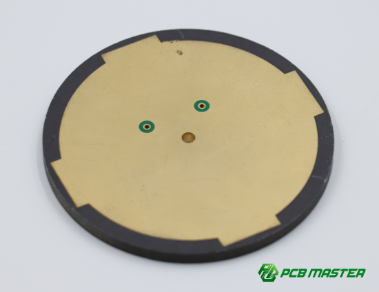
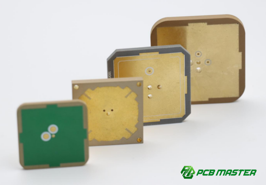
What is board shape and contour design in PCB outline design?
Board shape defines the physical boundary of the PCB, including standard and custom (irregular) shapes.
In PCB board shape design, the most common shapes are rectangular because they are easy to manufacture and cost-effective. However, many modern products require custom PCB outline design with curves, cutouts, or irregular edges to fit limited space.
For example:
l A router PCB may use a simple rectangle for easy assembly.
l A wearable device may require a curved or irregular PCB to match its enclosure.
Choosing the right shape is a balance between design flexibility and manufacturing efficiency. Complex outlines improve product integration but increase machining time and cost.
How to balance space utilization and manufacturing cost in PCB outline design?
Better space usage often increases manufacturing complexity and cost.
Using an irregular PCB shape can help maximize internal space, especially in compact devices. However, complex contours require CNC routing instead of simple stamping, which increases cost and production time.
Example comparison:
l Rectangular PCB → Low cost, fast production
l Irregular PCB → Better space fit, higher cost
A practical approach:
1. Start with a simple shape
2. Add cutouts only where necessary
3. Avoid excessive curves or small features
This helps achieve a balance between efficient PCB layout design and cost control.
What is the logic behind PCB corner design (right angle, chamfer, rounded)?
Corner design improves safety, assembly, and mechanical strength.
PCB corners are usually not perfectly sharp. Common options include:
l Right angle (R angle): Standard and low cost, typically with a small radius (e.g., R0.5mm)
l Chamfered corner: Used for insertion into slots (e.g., connector boards)
l Rounded corner: Reduces stress concentration and improves durability
For example, a PCB that slides into a connector must use a chamfer to avoid damage. A rounded corner is often used in consumer products to improve safety and appearance.
Good PCB corner design reduces cracking risk and improves handling during assembly.
How to choose PCB thickness in outline design?
PCB thickness affects strength, space, and application requirements.
Standard PCB thickness options include 0.8mm, 1.0mm, 1.2mm, and 1.6mm (most common). The choice depends on the product:
l Thin boards (≤1.0mm): Used in compact devices like wearables
l Standard boards (1.6mm): Used in most electronics
l Thick boards (≥2.0mm): Used for high power or structural support
Special cases:
l Metal core PCB: Better heat dissipation
l Flexible PCB: Extremely thin and bendable
Example: A power supply board may use a thicker PCB for strength and heat handling, while a smartwatch uses a thin PCB to save space.
How does PCB thickness affect impedance control?
PCB thickness directly impacts signal impedance in high-speed designs.
In controlled impedance PCB design, the distance between layers (which depends on board thickness) affects how signals travel. If the thickness changes, impedance also changes, which can cause signal loss or reflection.
| PCB Thickness Change | Structural Distance Change | Electrical Effect | Impedance Trend |
| Thicker board | Larger distance between layers | Lower capacitance | Higher impedance |
| Thinner board | Smaller distance between layers | Higher capacitance | Lower impedance |
Simple explanation:
Example: High-speed interfaces like USB or HDMI require precise impedance control. If the PCB thickness is incorrect, signals may become unstable.
This is why PCB stack-up design and thickness selection must be planned together early in the design stage.
What are PCBMASTER’s recommended outline dimensions and tolerance guidelines?
Proper dimensions and tolerances ensure reliable assembly and manufacturability.
PCBMASTER recommends the following PCB outline tolerance guidelines:
l General outline tolerance: ±0.2 mm
l Precision areas (connectors, slots): ±0.1 mm or tighter
l Minimum internal radius: Based on tool size (typically ≥0.5 mm)
l Slot width: ≥1.0 mm for standard routing
Example:
A USB connector opening requires tight tolerance (±0.1 mm). If the tolerance is too loose, the connector may not align with the enclosure.
Best practice:
1. Define critical dimensions early
2. Apply tighter tolerance only where needed
3. Follow DFM (Design for Manufacturability) rules
PCBMASTER supports customers by reviewing designs and optimizing PCB mechanical dimensions to reduce risk and improve production yield.
What Key Associated Features and Interface Designs Must Be Considered in PCB Outline Design?
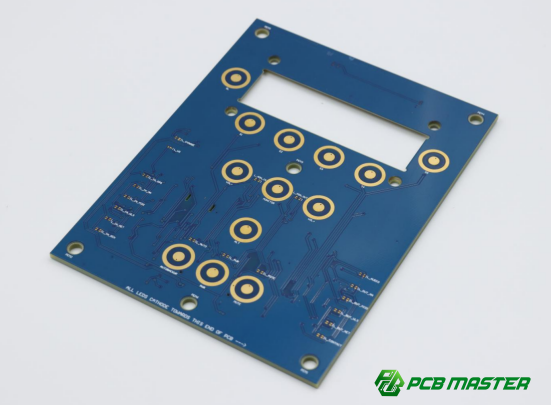
PCB outline design must include mounting holes, connector openings, slots, gold fingers, fiducials, and panelization features to ensure proper assembly, connection, and manufacturing.
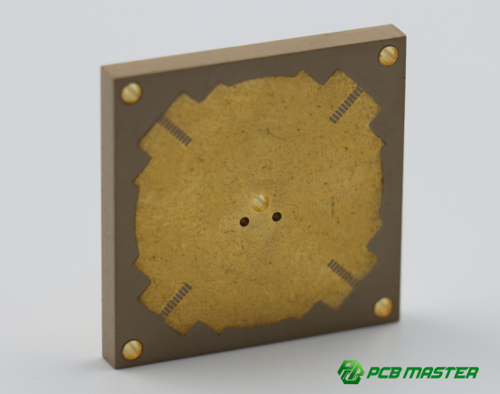
What are the key considerations in PCB mounting hole design?
Mounting holes must match the enclosure, have the correct size, and include keep-out areas to avoid interference.
In PCB mounting hole design, three factors are critical:
l Position accuracy: Holes must align exactly with enclosure standoffs
l Hole diameter: Typically = screw size + 0.2–0.5 mm clearance
l Non-plated holes (NPTH): Prevent electrical shorting with screws
Example:
If an M3 screw is used, the hole is usually designed as 3.2–3.5 mm.
Design steps:
1. Get enclosure drawing from mechanical engineer
2. Place holes based on exact coordinates
3. Add keep-out zones (no traces or components nearby)
Poor hole placement can cause assembly failure or board stress.
How to design connector openings for alignment and strength?
Connector openings must align precisely with external ports and maintain board strength.
In PCB connector cutout design, accuracy is critical. Openings for USB, HDMI, or power connectors must match the enclosure within tight tolerances (often ±0.1 mm).
Key points:
l Ensure exact position matching with enclosure openings
l Avoid placing cutouts near weak board edges
l Reinforce areas with connectors to prevent cracking
Example:
A misaligned USB port by even 0.3 mm can prevent cable insertion.
Best practice:
l Use 3D models (STEP files) for alignment
l Validate with mechanical team before production
This ensures both mechanical fit and long-term durability.
How do slots and irregular features affect PCB manufacturability and strength?
Slots and irregular shapes improve functionality but must follow machining limits to avoid damage.
PCB slot design is used for:
l Component adjustment (e.g., potentiometers)
l Airflow and heat dissipation
l Mechanical locking features
Key design rules:
l Minimum slot width: typically ≥1.0 mm
l Slot ends must be rounded (due to tool shape)
l Avoid sharp internal corners (cause stress concentration)
Example:
A ventilation slot improves cooling but too many slots can weaken the board.
Simple rule:
l Use slots only where necessary
l Keep shapes simple and smooth
This balances functionality, strength, and manufacturability.
What are the key requirements for PCB gold finger design?
Gold fingers must ensure reliable insertion, wear resistance, and precise dimensions.
PCB gold finger design is used in edge connectors (e.g., PCIe, memory modules).
Key requirements:
l Chamfered edge (usually 45°): Helps smooth insertion
l Hard gold plating: Improves wear resistance
l Strict thickness tolerance: Ensures proper contact
Example:
If the PCB is too thick, it may not fit into the slot. If too thin, contact becomes unreliable.
Design checklist:
l Define insertion direction
l Add chamfer at entry edge
l Specify gold plating thickness
Proper design ensures stable electrical connection and long service life.
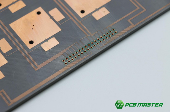
Why are fiducial marks critical in PCB assembly?
Fiducials help machines accurately locate the PCB during automated assembly.
In PCB fiducial design, these marks act as visual reference points for SMT machines.
Key guidelines:
l Place at least two global fiducials on opposite corners
l Use 1.0 mm copper pads with clear surrounding area
l Ensure high contrast (no solder mask nearby)
Example:
Without fiducials, components may be placed incorrectly, especially for fine-pitch ICs.
Additional tip:
l Add local fiducials near complex components (e.g., QFN, BGA)
This improves placement accuracy and assembly yield.
How do panelization and process edges improve PCB manufacturing efficiency?
Panelization groups multiple boards together, and process edges support handling during assembly.
In PCB panel design, small boards are combined into a larger panel to improve SMT efficiency.
Two common methods:
l V-CUT: Straight-line separation, fast and cost-effective
l Mouse bites (tab routing): Used for irregular shapes
Process edges (rails):
l Extra margins (usually ≥5 mm) added to panel sides
l Used for conveyor transport and fiducial placement
Example:
Without process edges, the board cannot be held by SMT machines.
Best practice:
l Choose panel method based on board shape
l Add rails for stability
l Place fiducials on rails
PCBMASTER helps optimize panel layout design to reduce cost and improve production speed.
How to Achieve Structural Compatibility and Manufacturability in PCB Outline Design (DFM)?
Structural compatibility and manufacturability in PCB outline design are achieved by aligning enclosure constraints, respecting manufacturing limits, controlling tolerances, selecting proper depaneling methods, and following a structured DFM review process.
What is the PCB and enclosure co-design method?
It is a collaborative design process where PCB outline and mechanical enclosure are developed together to ensure perfect fit.
In PCB enclosure co-design (mechanical-electrical co-design), the PCB shape is not designed alone. It must match the 3D mechanical housing.
Key steps:
1. Mechanical engineer provides enclosure CAD model (STEP file)
2. PCB designer defines board outline based on internal space
3. Connector positions and mounting holes are aligned together
4. Iterative adjustment between ME and EE teams
Example:
In a router, the Ethernet ports are fixed by the enclosure. The PCB outline must shift to match exact port positions. If not aligned, assembly will fail.
This method ensures PCB mechanical compatibility and assembly success rate.
What manufacturing limitations affect PCB outline design?
PCB outline design is limited by tool size, routing radius, and minimum manufacturable structure dimensions.
In PCB manufacturing constraint design, three main limits must be considered:
l Router bit (milling tool) radius: Typically ≥0.5 mm
l Minimum slot width: Usually ≥1.0 mm
l Sharp corners cannot be perfectly made: Must use rounded edges
Example:
A sharp internal 90° corner is not manufacturable. It must be replaced with a curved radius based on tool size.
Simple rule:
l If the tool cannot cut it → the design must change
l Ignoring these limits may cause:
l Board cracking
l Production failure
l Increased cost due to rework
How to control PCB outline tolerances and accuracy levels?
Tolerance control ensures that different PCB features meet required precision levels based on function.
In PCB tolerance design, not all areas need the same precision.
Common tolerance levels:
l General outline: ±0.2 mm
l Mounting holes / connectors: ±0.1 mm
l High-precision interfaces: even tighter if required
Example:
A USB port opening needs higher precision than a board edge because it directly affects plug alignment.
Design strategy:
l Identify critical functional areas
l Assign tight tolerances only where needed
l Use standard tolerances elsewhere to reduce cost
This approach balances cost efficiency and assembly accuracy.
What is the difference between V-CUT and mouse bites in PCB panel design?
V-CUT is used for straight-line separation, while mouse bites are used for irregular shapes.
| Feature | V-CUT (V-groove) | Mouse Bites (Tab Routing) |
| Cutting method | Straight groove cut | Small perforated tabs |
| Board shape | Rectangular boards | Irregular or curved boards |
| Edge quality | Clean but straight | Slightly rough edges |
| Cost | Lower | Higher |
| Flexibility | Low | High |
Example:
l Smartphone PCB panels → often use mouse bites for irregular shapes
l LED driver boards → often use V-CUT for simple rectangular separation
Selection rule:
l Use V-CUT for simplicity and cost efficiency
l Use mouse bites for complex PCB outline shapes
What is PCBMASTER’s DFM review and optimization process?
PCBMASTER ensures manufacturability by reviewing PCB outline design, identifying risks, and optimizing structure before production.
PCBMASTER’s DFM (Design for Manufacturability) process includes:
Step 1: File review
Check PCB outline, holes, slots, and tolerances
Step 2: Manufacturing feasibility check
Validate routing limits, tool access, and panel design
Step 3: Risk identification
Detect sharp corners, weak structures, or misaligned interfaces
Step 4: Optimization suggestions
Adjust outline, improve strength, reduce cost
Step 5: Final confirmation before production
Example:
A customer design with sharp internal corners was modified to rounded radii to prevent cracking during manufacturing.
This process helps improve:
l Production yield
l Structural reliability
l Cost efficiency
PCBMASTER focuses on delivering production-ready PCB outline designs through structured DFM validation.
How Does PCB Outline Design Affect Reliability, Electrical Performance, and Heat Dissipation?
PCB outline design directly affects mechanical strength, signal stability, safety distance, and thermal performance by defining how the board physically behaves inside the product.
How does mechanical strength design prevent stress concentration and cracking in PCB outline design?
Mechanical strength design reduces weak points in the PCB outline to prevent cracking under pressure or vibration.
In PCB mechanical strength design, stress often appears at sharp corners, cutouts, and connector areas. These locations can become failure points if not designed properly.
Key rules:
l Avoid sharp internal corners (use rounded radii instead)
l Add fillets near slots and cutouts
l Keep mounting holes away from board edges when possible
Example:
A PCB with a sharp 90° internal corner may crack during vibration testing. Changing it to a rounded corner distributes stress more evenly.
Simple idea:
Smooth shapes = lower stress = higher reliability
This is a core part of reliable PCB outline design for industrial applications.
How does PCB warpage control and structural symmetry improve reliability?
Symmetrical PCB outline and balanced structure reduce bending and warping during manufacturing and operation.
PCB warpage control design focuses on preventing the board from bending due to uneven stress or heat.
Key principles:
l Keep PCB shape as symmetrical as possible
l Avoid long narrow extensions without support
l Balance copper distribution across the board
Example:
A long, uneven PCB used in LED lighting may bend after reflow soldering. Adding symmetry reduces this effect.
Comparison:
l Symmetrical board → stable, flat
l Asymmetrical board → higher risk of warping
This improves assembly accuracy and long-term reliability.
How does PCB edge creepage distance affect high-voltage safety design?
PCB edge creepage distance ensures safe electrical isolation between high-voltage conductors and board edges.
In high-voltage PCB outline design, creepage distance is the path along the surface of the PCB between two conductors.
Key points:
l Maintain safe distance between high-voltage traces and board edge
l Increase spacing in humid or polluted environments
l Follow safety standards (IPC, IEC guidelines)
Example:
In a power supply PCB, insufficient creepage distance can cause electrical arcing near the board edge.
Simple rule:
Higher voltage → larger creepage distance required
This is critical for safe PCB outline design in power electronics and industrial systems.
How does PCB outline design affect heat dissipation paths?
PCB shape influences how heat spreads and transfers to the environment or enclosure.
In PCB thermal design, the outline affects airflow, heat spreading, and contact with heat sinks.
Key factors:
l Larger metal contact area improves heat transfer
l Open cutouts can improve airflow
l Mounting points can connect to metal chassis for cooling
Example:
A power PCB with a flat surface connected to a metal enclosure can dissipate heat more efficiently than a fully enclosed board.
Design strategy:
l Align hot components near thermal paths
l Use mounting holes for heat conduction
l Avoid blocking airflow with dense outlines
This improves thermal reliability and component lifespan.
What is PCBMASTER’s experience in high-reliability PCB outline design?
PCBMASTER applies mechanical, electrical, and thermal design rules together to ensure stable and reliable PCB performance in real applications.
PCBMASTER focuses on high-reliability PCB outline design across industries such as automotive, industrial control, and power systems.
Core practices:
l Stress analysis of sharp edges and cutouts
l Warpage control through balanced PCB structure
l Safety validation of creepage distances for high voltage
l Thermal path optimization for heat-sensitive designs
Example case:
In an industrial power control board, PCBMASTER optimized the outline by:
Rounding high-stress corners
l Increasing creepage distance near power zones
l Adding thermal contact areas to the metal chassis
Result:
Improved durability, lower failure rate, and better thermal stability.
This approach ensures robust PCB mechanical design for real-world conditions.
What Industry Standards and Practical Guidelines Must PCB Outline Design Follow?
PCB outline design must follow IPC standards and industry-specific rules to ensure correct dimensions, safe structure, and reliable mass production.
What does IPC-2615 define in PCB size and tolerance standards?
IPC-2615 defines how PCB dimensions and tolerances should be controlled to ensure manufacturability and assembly accuracy.
In PCB size and tolerance standards (IPC-2615), the focus is on controlling the physical accuracy of the PCB outline and key mechanical features.
Key points:
l Defines acceptable outline dimensional tolerance (e.g., ±0.1 mm to ±0.2 mm)
l Covers accuracy of holes, slots, and board edges
l Ensures PCB fits properly into enclosure and assembly fixtures
Example:
A PCB designed for a plastic enclosure must match standoff positions. If tolerance is too loose, screws may not align during assembly.
Simple rule:
Tighter tolerance = higher precision = higher manufacturing cost
This standard is widely used in PCB mechanical design for mass production and high-precision assembly.
What are the basic structural rules defined in IPC-2221?
IPC-2221 provides general design rules for PCB structure, spacing, and safety to ensure electrical and mechanical reliability.
In IPC-2221 PCB design guidelines, the focus is on safe spacing and structural integrity.
Key rules include:
l Minimum spacing between conductors to avoid short circuits
l Clearance rules for high-voltage areas
l General mechanical layout safety guidelines
Example:
In a power PCB, high-voltage traces must be separated from board edges and low-voltage areas to prevent arcing.
Simple explanation:
More voltage = more spacing required
This standard is essential for safe PCB outline and layout design in power and industrial electronics.
What special requirements exist for automotive and medical PCB outline design?
Automotive and medical PCBs require higher reliability, stricter tolerances, and stronger environmental resistance.
Different industries have different PCB outline design requirements:
Automotive PCB requirements:
Must withstand vibration, shock, and temperature cycles
l Strong mechanical mounting design
l High reliability over long product life
Example:
A car ECU PCB must survive engine vibration and extreme temperature changes.
Medical PCB requirements:
l High precision and safety compliance
l Stable long-term operation
l Strict quality control and traceability
Example:
A medical monitoring device PCB must ensure stable signal output without failure.
Comparison:
l Automotive → durability and vibration resistance
l Medical → precision and safety stability
Why is it important to apply standards during the PCB design stage?
Applying standards early reduces redesign risk, improves manufacturability, and lowers production cost.
In PCB design workflow optimization, standards should not be applied at the end—they must be integrated at the beginning.
Key benefits:
l Prevents layout and mechanical conflicts early
l Reduces costly redesign after prototyping
l Improves DFM (Design for Manufacturability) success rate
Example:
If IPC spacing rules are ignored early, the board may pass schematic review but fail during manufacturing.
Simple workflow:
1. Apply IPC rules during initial design
2. Validate with mechanical constraints
3. Perform DFM check before production
This ensures efficient PCB development and stable mass production.
What is PCBMASTER’s standardized PCB outline design checklist?
Short Answer: PCBMASTER uses a structured checklist to ensure all PCB outline designs meet mechanical, electrical, and manufacturing standards.
PCBMASTER’s PCB design checklist (standardized DFM review process) includes:
1. Mechanical structure check
l Board shape feasibility
l Edge strength and stress points
l Mounting hole alignment
2. Manufacturing check
l Routing limits and tool accessibility
l Minimum slot and radius verification
l Panelization suitability
3. Electrical safety check
l Creepage and clearance compliance
l High-voltage spacing validation
4. Assembly check
l Connector alignment accuracy
l Fiducial and SMT compatibility
Example:
A design with sharp corners and tight connector spacing was modified by PCBMASTER to improve manufacturability and reduce cracking risk.
This checklist ensures high-quality, production-ready PCB outline design for global manufacturing standards.
Conclusion
PCB outline design is the key link between mechanical structure and electrical performance. A PCB must not only carry circuits, but also fit precisely into the enclosure, align with connectors, and meet manufacturing requirements. When the board shape, mounting holes, and interface openings are properly designed, the product becomes easier to assemble, more reliable, and less prone to mechanical or electrical issues.
In practice, many failures come from poor PCB mechanical design—such as misaligned ports, weak corners, or incorrect board dimensions. A well-optimized outline helps avoid these problems by balancing space usage, structural strength, and manufacturability. This makes PCB outline design a critical part of turning an electronic concept into a stable mass-production product.
PCBMASTER supports customers with professional PCB outline optimization and DFM review. By checking structure, manufacturing limits, and assembly compatibility early in the design stage, PCBMASTER helps reduce design risks, improve production yield, and ensure high-quality final products across consumer, industrial, and automotive applications.
FAQs
How should PCB outline tolerances be reasonably defined?
PCB outline tolerances should be defined based on function, not uniformly across the entire board.
In PCB tolerance design, different features require different accuracy levels. A common practice is:
l General board outline: ±0.2 mm
l Mounting holes and connectors: ±0.1 mm
l High-precision interfaces: even tighter if needed
For example, a USB port area needs higher precision than a simple board edge because it directly affects assembly alignment. Over-tightening all tolerances increases cost without real benefit, while loose tolerances can cause assembly failure. The key is to apply PCB manufacturing tolerance control (DFM principle) only where it matters.
Does irregular PCB (custom shape) always increase cost?
No, but irregular PCB shapes usually increase manufacturing complexity, which may increase cost.
In custom PCB outline design, cost depends on complexity:
l Simple rectangle → lowest cost, fastest production
l Moderate irregular shape → slight cost increase
l Highly complex shape with many cutouts → higher CNC routing cost
For example, a wearable device may need a curved PCB to fit the enclosure. This improves product design but requires more routing time and tooling.
Best practice:
Use irregular shapes only when necessary for space or function. This helps balance PCB design optimization and manufacturing cost control.
Must PCB mounting holes always be non-plated?
No, mounting holes can be plated or non-plated depending on electrical and mechanical needs.
In PCB mounting hole design:
l Non-plated holes (NPTH): used for mechanical fixing, safer for insulation
l Plated holes (PTH): used when grounding or electrical connection is required
For example:
l Plastic enclosure → NPTH is commonly used
l Metal chassis grounding → PTH may be required
Incorrect selection can cause short circuits or poor grounding. The key is to define the function of each hole during PCB structural design stage.
What problems can poor gold finger chamfer design cause?
Incorrect gold finger chamfer design can cause insertion failure, wear damage, or poor electrical contact.
In PCB gold finger design, the chamfer (usually 30°–45°) helps guide the board into a connector smoothly.
Common issues:
l No chamfer → difficult insertion, connector damage risk
l Incorrect angle → misalignment or scratching
l Poor plating → fast wear and unreliable contact
For example, in memory modules or PCIe cards, poor chamfer design can cause repeated insertion failure or signal instability.
Proper design ensures smooth insertion, long service life, and stable electrical connection.
How does PCB panel design affect SMT efficiency and yield?
Poor panel design can reduce SMT efficiency, while optimized panelization improves production speed and yield.
In PCB panelization design, multiple boards are combined into one panel for SMT processing.
Impact on SMT:
l Good panel design → stable transport, fast assembly, high yield
l Poor panel design → vibration, misalignment, lower placement accuracy
Common methods:
l V-CUT panels: fast and cost-effective for rectangular boards
l Mouse bites (tab routing): flexible for irregular shapes
For example, a poorly supported panel may bend during reflow, causing solder defects.
Proper PCB panel design optimization improves:
l SMT machine efficiency
l Assembly stability
l Final product yield

