


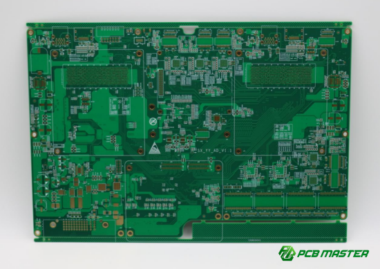
PCB Design and Layout Tips for High-Performance Electronic Circuits
High-performance electronics leave no room for layout mistakes. As operating speeds increase and component density rises, PCB design becomes less about basic connectivity and more about controlling signals, power stability, and electromagnetic behavior with precision.
Even a small routing decision can affect signal integrity, thermal performance, or overall system reliability. That is why engineers rely on proven layout strategies to ensure circuits operate cleanly under high-speed and high-frequency conditions.
With years of experience in PCB design and manufacturing, PCBMASTER shares practical, engineering-focused insights into real-world high-performance PCB layout practices. This article covers key areas such as stack-up planning, component placement, routing strategies, and EMI control, breaking down critical design decisions that directly impact performance, reliability, and manufacturability, and helping engineers avoid common pitfalls while achieving stable, production-ready results.
What Are the Core Principles of High-Performance PCB Design and Layout?
High-performance PCB design is mainly based on three core principles: signal integrity, power integrity, and thermal management. These three areas work together to ensure the circuit runs fast, stable, and without interference. If any one of them is ignored, the whole system can become unstable, especially in high-speed or high-power electronics.
Signal Integrity Requirements in High-Speed Circuits
Signal integrity means keeping electrical signals clean, fast, and accurate as they move through the PCB without distortion or delay.
In high-speed PCB design and layout, signals travel very quickly across traces. If the design is poor, the signal can become “dirty,” meaning it loses shape or timing. This is called signal distortion, and it can cause communication errors between chips.
Controlled impedance and clean signal transitions
Controlled impedance means designing PCB traces so that the signal sees a consistent electrical environment. This is very important in high-speed PCB layout design, such as USB, DDR memory, or RF circuits.
For example, if a trace is not controlled properly, the signal may bounce back instead of moving forward smoothly. PCB engineers usually adjust trace width, spacing, and layer stack-up to match impedance. This helps signals move like a smooth road instead of a bumpy path.
Avoiding reflection, overshoot, and timing distortion
When impedance is not controlled, signals can reflect back like an echo. This is called signal reflection, and it can cause data errors.
Overshoot happens when a signal goes higher than expected, while undershoot goes too low. Both can damage signal accuracy.
For example, in a high-speed memory circuit, even a small reflection can cause wrong data reading. That is why PCBMASTER applies strict routing rules like short trace length, proper termination, and matched signal paths to avoid timing issues in high-speed electronic PCB design.
Power Integrity and Stable Voltage Delivery
Power integrity means delivering clean and stable voltage to all components without noise or voltage drops.
Even if signals are perfect, unstable power can still crash the system. In high-performance PCB design and layout, power must stay steady even when chips switch quickly between high and low states.
Decoupling strategy for high-speed ICs
Decoupling capacitors are small components placed near IC power pins. Their job is to supply instant energy when the chip suddenly needs power.
A simple way to understand this: imagine a water tank supplying water to a house. If the pipe is too long, water pressure drops. Decoupling capacitors act like a small local tank close to the chip.
For example, in CPU or FPGA boards, multiple capacitors of different sizes are placed together. Small capacitors handle fast noise, while larger ones handle bigger energy changes. This is a key rule in PCB power integrity design.
Reducing voltage drop and transient noise
Voltage drop happens when power has to travel too far through thin traces. This can make chips unstable or reset unexpectedly.
Transient noise is sudden unwanted voltage spikes caused by fast switching.
To solve this, PCB designers use wide power traces, solid power planes, and short return paths. PCBMASTER often uses multi-layer power planes in PCB layout for stable power distribution to ensure every chip receives clean voltage.
Thermal Management in Dense PCB Structures
Thermal management means controlling heat so the PCB does not overheat and fail during operation.
Modern electronic circuits generate heat, especially in power supplies, processors, and LED drivers. If heat is not controlled, it can damage components or reduce product life.
Heat distribution through copper and vias
Copper is a good heat conductor. In PCB design, copper planes help spread heat across the board instead of letting it stay in one spot.
Vias (small plated holes) also help transfer heat between layers. These are called thermal vias.
For example, in a power circuit, placing thermal vias under a voltage regulator helps move heat to inner copper layers, making the board cooler and more stable. This is a common method in high-power PCB thermal design.
Avoiding hotspots in power-dense areas
Hotspots happen when too much heat is concentrated in one small area. This usually happens near power ICs or switching components.
To avoid this, designers spread components out, increase copper area, and use heat sinks when needed. In some cases, airflow direction is also considered during PCB layout planning.
PCBMASTER applies thermal simulation and layout optimization in PCB design for high-power electronics to ensure stable operation even under heavy load conditions.
How Should PCB Stack-Up and Component Placement Be Designed for Optimal Performance?
PCB stack-up and component placement should be designed to control noise, shorten signal paths, and maintain stable grounding so that high-speed circuits can operate reliably and efficiently.
In high-performance PCB design and layout, stack-up and placement are not just structural choices—they directly affect signal quality, power stability, and EMI performance. A well-planned structure reduces interference and improves overall circuit speed and reliability.
Multi-Layer Stack-Up Design for Signal and Noise Control
A proper PCB stack-up uses multiple layers of signal, ground, and power planes to control noise and maintain stable high-speed signal transmission.
In modern multi-layer PCB design, stack-up defines how layers are arranged inside the board. Good layer planning helps reduce electromagnetic interference (EMI) and improves signal integrity in high-speed circuits.
Ground/power plane configuration for stability
A stable PCB stack-up usually includes continuous ground and power planes placed close to signal layers. This creates a low-noise environment for signals.
For example, in a 6-layer PCB, a common structure is:
l Top signal layer
l Ground plane
l Power plane
l Ground plane
l Signal layer
l Bottom layer
This structure helps reduce noise because the ground plane acts like a shield. In PCB layout design for high-speed electronics, this is essential for stable operation of CPUs, memory chips, and RF modules.
Microstrip vs. stripline selection for high-speed routing
There are two common routing structures: microstrip and stripline.
| Routing Type | Structure | Key Characteristics | Advantages | Disadvantages | Typical Use Cases |
| Microstrip Routing | Signal trace placed on the outer PCB layer (above a ground plane) | Signal is exposed to air and nearby components | Easier to design and manufacture; lower cost; simpler debugging | More sensitive to noise and EMI; higher signal loss at high frequency | Low to medium-speed signals, general digital circuits |
| Stripline Routing | Signal trace embedded inside PCB between two ground planes | Signal is fully surrounded by dielectric and shielding planes | Excellent noise immunity; better signal integrity; stable impedance control | More complex design; higher manufacturing cost; harder to access for testing | High-speed signals (DDR, USB, RF, high-frequency systems) |
For example, in USB or DDR memory design, stripline is often used because it reduces interference. PCBMASTER often chooses stripline routing in high-speed PCB stack-up design when signal quality is critical.
Strategic Component Placement for Signal Efficiency
Component placement should minimize signal travel distance and separate different circuit types to improve speed, reduce noise, and increase stability.
In PCB component placement optimization, location matters as much as routing. Poor placement leads to longer traces, higher delay, and more noise.
Minimizing critical signal path length
Short signal paths mean faster and cleaner communication between components.
For example, in a CPU + memory system, placing memory chips close to the processor reduces delay and improves performance. Long traces act like slow roads, causing timing issues.
A simple rule used in high-speed PCB layout design is: place connected components as close as functionally possible before routing begins.
Separating analog, digital, and power domains
Different circuit types behave differently. Mixing them can cause interference.
l Analog circuits are sensitive to noise
l Digital circuits switch fast and generate noise
l Power circuits carry high current
For example, in an audio PCB, placing digital switching circuits near analog audio paths can cause noise in the sound output.
That is why PCBMASTER applies domain separation in PCB layout design, grouping similar circuits together and isolating sensitive areas for clean performance.
Grounding Strategy for Stable Circuit Performance
A good grounding strategy ensures stable reference voltage and provides a clean return path for all signals in the PCB.
Ground is the foundation of every electronic circuit. In PCB grounding design, poor grounding is one of the main causes of noise, instability, and EMI issues.
Continuous ground plane design
A continuous ground plane means using a solid copper layer without breaks or splits.
This helps because all components share the same reference point. If the ground plane is broken, signals lose stability and noise increases.
For example, in high-speed USB design, a continuous ground plane ensures data signals remain clean and stable during transmission.
PCBMASTER always recommends continuous ground planes in high-performance PCB layout design to improve noise resistance and circuit stability.
Return path optimization for high-speed signals
Every signal needs a return path. If the return path is long or interrupted, noise and EMI increase.
In high-speed circuits, signals travel forward while return current follows the ground plane directly underneath the trace. If the ground is split, the return path detours, creating interference.
For example, in DDR memory routing, maintaining a direct return path is critical for timing accuracy.
In advanced PCB layout design, PCBMASTER ensures that return paths are short, direct, and aligned with signal traces to maintain stable high-speed performance.
What Are the Best Routing and Noise Control Techniques in PCB Layout?
The best routing and noise control techniques in PCB layout focus on keeping signals clean, reducing interference between traces, and ensuring stable power delivery across the board.
In high-performance PCB design and layout, routing and noise control directly affect signal accuracy, EMI performance, and system stability. Good layout practices reduce errors before manufacturing, saving cost and redesign time.
High-Speed Routing Rules for Signal Integrity
High-speed routing rules ensure signals travel with correct timing and shape by controlling trace length, geometry, and path consistency.
In high-speed PCB routing design, even small layout mistakes can cause data errors or signal distortion. The goal is to keep signals fast, stable, and predictable.
Differential pair matching and trace length control
Differential pairs are two signals that carry opposite signals (like USB or Ethernet). They must be exactly matched in length so both signals arrive at the same time.
If one trace is longer, it causes timing mismatch, which reduces signal quality. This is called skew.
For example, in USB 3.0 PCB design, even a small length difference can cause communication errors. That is why PCBMASTER uses strict trace length matching rules in high-speed PCB layout design to ensure stable data transmission.
Avoiding sharp bends and unnecessary vias
Sharp 90-degree bends can create signal reflection points. Instead, smooth 45-degree bends are used to maintain signal flow.
Vias (holes connecting layers) also add resistance and delay. Too many vias can weaken signal strength.
For example, in DDR memory routing, minimizing vias helps improve timing accuracy. PCB designers often follow the rule: short, straight, and clean routing paths for high-speed signals.
Crosstalk and EMI Reduction Techniques
Crosstalk and EMI reduction techniques aim to prevent signals from interfering with each other by controlling spacing, shielding, and layer structure.
In PCB noise reduction design, unwanted electromagnetic coupling can cause signal distortion or system instability.
Proper trace spacing and layer isolation
When two signal traces are too close, they can “talk” to each other. This is called crosstalk.
A simple example: think of two people whispering very close together—you may hear the wrong message.
To avoid this, designers increase spacing between high-speed traces and separate noisy and sensitive signals into different layers.
For example, digital switching signals should not run next to analog audio traces. PCBMASTER applies layer isolation techniques in PCB layout design to reduce interference and improve clarity.
Guard traces and shielding strategies
A guard trace is a grounded trace placed between two signal lines to block interference.
Shielding works like a protective wall, absorbing or redirecting noise.
For example, in RF PCB design, sensitive antenna signals are often surrounded by ground shielding to prevent external noise.
In high-performance PCB EMI control design, PCBMASTER uses guard traces and grounded copper pours to stabilize signal quality in dense layouts.
Power Distribution and Decoupling Optimization
Power distribution and decoupling optimization ensure that every component receives clean, stable power without voltage drops or noise spikes.
In PCB power integrity design, unstable power is one of the most common causes of system failure.
Efficient PDN (Power Distribution Network) design
A Power Distribution Network (PDN) is the system that delivers power across the PCB.
A good PDN uses wide traces or full power planes to reduce resistance and voltage drop.
For example, in CPU boards, power must reach all cores evenly. If the PDN is weak, the system may restart or crash under load.
PCBMASTER uses optimized PDN design in high-performance PCB layout to ensure stable voltage delivery even during fast switching operations.
Capacitor placement hierarchy and placement rules
Decoupling capacitors act like local energy buffers near ICs. They supply instant current when needed.
A good rule is:
l Small capacitors (0.1µF) → close to IC pins for high-frequency noise
l Medium capacitors (1–10µF) → stabilize mid-frequency changes
l Large capacitors → support overall power stability
For example, in Field-Programmable Gate Array (FPGA) design, multiple capacitor sizes are placed together in a layered structure to handle different noise frequencies.
In PCB decoupling capacitor layout design, PCBMASTER ensures capacitors are placed as close as possible to power pins to minimize noise and improve response speed.
What Common PCB Design Mistakes Should Be Avoided in High-Performance Applications?
The most common PCB design mistakes include poor layout planning, weak grounding and power design, and ignoring EMI and thermal issues. These mistakes can cause signal errors, instability, and even system failure.
In high-performance PCB design and layout, avoiding these problems early is critical. Fixing them after manufacturing is expensive and time-consuming. Below are the key mistakes and how to understand them in simple terms.
Poor Layout Planning and Component Misplacement
Poor layout planning increases signal delay and noise, especially when components are placed too far apart or grouped incorrectly.
In PCB layout design for high-speed circuits, placement should always be done before routing. A bad layout creates problems that routing cannot fix later.
Long signal paths increasing delay and noise
Long traces act like long wires—they slow down signals and pick up noise from the environment.
For example, if a processor is placed far away from memory, the signal takes longer to travel. This can cause timing errors in high-speed systems like DDR or FPGA boards.
A simple rule in high-speed PCB design is: keep critical components close together to shorten signal paths and reduce delay.
Mixing high-speed and low-speed circuits improperly
High-speed circuits switch very fast and generate noise. Low-speed or analog circuits are more sensitive to interference.
If they are placed together without separation, noise can leak into sensitive signals.
For example, placing a switching power supply next to an audio circuit can create unwanted noise in sound output.
PCBMASTER avoids this by using functional block separation in PCB layout design, grouping similar circuits and isolating sensitive areas.
Weak Grounding and Power Design Practices
Weak grounding and poor power design lead to unstable signals, voltage noise, and system crashes.
In PCB power and grounding design, the ground and power system must be strong, continuous, and well-planned.
Broken ground planes causing instability
A ground plane should be solid and continuous. If it is split or broken, signals lose a stable reference point.
This can cause noise, EMI, and unpredictable behavior.
For example, if a high-speed signal crosses a gap in the ground plane, its return path is interrupted, increasing interference.
In high-performance PCB layout, PCBMASTER always maintains continuous ground planes to ensure signal stability.
Insufficient decoupling leading to noise issues
Without enough decoupling capacitors, ICs cannot get stable power during fast switching.
This causes voltage dips and noise, which may lead to system resets or data errors.
For example, in FPGA or CPU boards, missing or poorly placed capacitors can cause unstable operation under load.
A good practice in PCB power integrity design is placing capacitors close to power pins and using multiple values to cover different noise frequencies.
Ignoring EMI and Thermal Constraints
Ignoring EMI and thermal factors can cause interference problems and overheating, reducing system reliability and lifespan.
In high-performance PCB layout design, EMI and heat must be considered from the beginning, not after the design is finished.
Excessive electromagnetic interference in dense layouts
Dense PCBs with fast signals can generate strong electromagnetic fields.
If not controlled, these fields interfere with nearby signals and cause communication errors.
For example, in wireless communication boards, EMI can reduce signal quality or fail compliance tests.
PCBMASTER applies EMI control techniques in PCB design, such as proper spacing, grounding, and shielding, to reduce interference.
Overheating due to poor thermal design
High-power components generate heat. If heat is not removed, components can fail or degrade over time.
For example, a voltage regulator without proper heat dissipation may overheat and shut down the system.
Solutions include adding copper area, thermal vias, and proper airflow design.
In PCB thermal management design, PCBMASTER ensures heat is evenly distributed and removed efficiently to maintain stable operation.
Why Choose PCBMASTER for High-Performance PCB Design and Manufacturing?
PCBMASTER combines engineering expertise, advanced manufacturing technology, and full-service support to deliver reliable, high-performance PCB and PCBA solutions.
In high-performance PCB design and manufacturing, choosing the right partner is critical. A strong supplier not only builds the board but also helps prevent design issues, improve performance, and reduce overall project risk.
Engineering Expertise in High-Speed PCB Layout
PCBMASTER provides deep engineering experience in high-speed PCB design, ensuring stable signal performance and reliable circuit behavior.
Experience with multilayer and HDI designs
PCBMASTER has extensive experience in multilayer PCB design and HDI (High-Density Interconnect) PCB layout. These designs are commonly used in complex electronics like communication systems, industrial control boards, and AI hardware.
For example, in a 10-layer high-speed PCB, proper layer stack-up and routing strategy are critical. PCBMASTER engineers understand how to structure layers, control impedance, and manage signal flow in dense layouts.
This experience reduces design errors and ensures the board performs correctly in real-world conditions.
Optimization for signal and power integrity
PCBMASTER focuses on signal integrity and power integrity optimization during the design stage.
This includes:
l Controlled impedance routing
l Proper grounding and return paths
l Stable power distribution network (PDN)
For example, in FPGA-based systems, unstable power or poor routing can cause system crashes. PCBMASTER applies proven design rules to ensure signals remain clean and power remains stable in high-speed PCB layout design.
Advanced Manufacturing Capabilities
PCBMASTER uses advanced fabrication processes to produce high-precision PCBs that meet strict performance and quality requirements.
Precision fabrication for complex PCB structures
High-performance PCBs often require tight tolerances, fine trace widths, and complex structures.
PCBMASTER supports:
l Fine line and spacing
l Controlled impedance manufacturing
l HDI structures with microvias
For example, in RF or high-frequency PCB design, even small manufacturing errors can affect signal quality. PCBMASTER ensures precision fabrication to match the design requirements exactly.
This is essential for high-frequency and high-speed PCB manufacturing.
Support for prototypes and mass production
PCBMASTER provides flexible production services, from small prototype runs to large-scale manufacturing.
For example:
l Engineers can test early designs with prototypes
l Once validated, the same design can move to mass production smoothly
This reduces risk and speeds up product development.
In PCB prototyping and volume production, PCBMASTER ensures consistency between test boards and final products.
Full PCB and PCBA Turnkey Support
PCBMASTER offers complete end-to-end services, from design review to final assembly, helping customers save time and reduce complexity.
Design optimization before fabrication
Before production, PCBMASTER reviews the design to identify potential issues.
This includes:
l Checking layout for signal integrity risks
l Verifying power and grounding structure
l Suggesting improvements for manufacturability
For example, a design with poor via placement or tight spacing may cause manufacturing defects. Early optimization prevents costly redesigns.
This step is critical in DFM (Design for Manufacturability) in PCB design.
End-to-end engineering and production services
PCBMASTER provides full PCB and PCBA turnkey solutions, including:
l PCB fabrication
l Component sourcing
l Testing and quality control
For example, instead of working with multiple suppliers, customers can rely on one partner to handle the entire process. This improves efficiency and communication.
In complete PCB assembly services, PCBMASTER ensures quality control at every stage, delivering reliable boards ready for final product integration.
Conclusion
High-performance PCB design and layout is not just about following rules—it’s about making the right decisions at every stage, from stack-up and routing to power, grounding, and thermal control. Small improvements in design can lead to big gains in reliability, speed, and overall product quality.
By applying these practical techniques and avoiding common mistakes, you can build PCBs that perform consistently even in demanding environments. And with the right partner, the process becomes faster, safer, and more efficient.
At PCBMASTER, we combine engineering expertise with advanced manufacturing to help you turn complex designs into high-quality, production-ready boards. Whether you are developing a prototype or scaling to mass production, we are here to support your high-performance PCB projects every step of the way.
Frequently Asked Questions About PCB Design and Layout
What is the most important factor in high-performance PCB design?
The most important factor is maintaining signal integrity and power integrity throughout the PCB.
In high-performance PCB design, signals must travel cleanly and power must remain stable. If signals are distorted or power fluctuates, the system may fail even if all components are correct. For example, in high-speed circuits like DDR or FPGA systems, poor signal integrity can cause data errors, while unstable power can lead to system crashes. That’s why designers focus on controlled impedance, proper grounding, and stable power delivery first.
How many layers are recommended for high-speed PCB designs?
Most high-speed PCB designs require at least 4 to 6 layers, but complex systems may need more.
Layer count depends on signal speed, circuit complexity, and power requirements. A simple high-speed board may use 4 layers (signal, ground, power, signal), while more advanced designs like networking or FPGA boards often use 6 to 12 layers. More layers allow better separation of signals, dedicated ground planes, and improved noise control. In general, more layers mean better performance but higher cost.
Why is decoupling capacitor placement so critical?
Decoupling capacitors provide instant local power and reduce noise near ICs.
When a chip switches quickly, it needs immediate current. If the power has to travel too far, voltage drops and noise occur. Decoupling capacitors act like small local energy storage units placed close to the chip. For example, placing a capacitor far from the IC reduces its effectiveness. Proper placement—very close to power pins—helps maintain stable voltage and reduces high-frequency noise in PCB power integrity design.
How can EMI be effectively reduced in PCB layouts?
EMI can be reduced by controlling layout, grounding, and signal routing.
Key methods include:
l Using continuous ground planes
l Keeping signal traces short and well-spaced
l Separating noisy and sensitive circuits
l Adding shielding or guard traces
For example, placing high-speed signals over a solid ground plane helps contain electromagnetic fields. In dense layouts, proper spacing and layer isolation are critical to prevent interference. These techniques are widely used in PCB EMI reduction design.
What advantages does PCBMASTER provide for complex PCB projects?
PCBMASTER provides engineering expertise, advanced manufacturing, and full turnkey support.
PCBMASTER helps customers handle complex PCB challenges by offering:
l Professional high-speed PCB layout optimization
l Support for multilayer and HDI designs
l Precision manufacturing for tight tolerances
l Full PCB and PCBA services from design to assembly
For example, in a complex FPGA project, PCBMASTER can review the layout, improve signal routing, and ensure manufacturability before production. This reduces risk and improves final product quality in high-performance PCB projects.

