


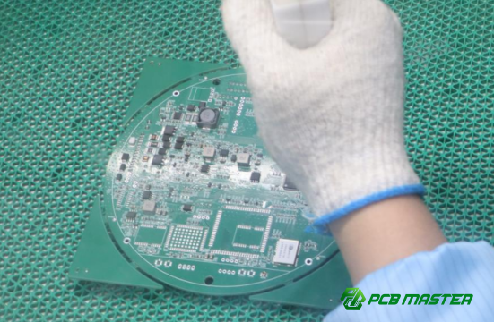
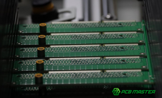
Common PCB Manufacturing Defects and How to Prevent Them – Insights from PCBMASTER
PCB manufacturing is a precise process, and even small errors can significantly affect performance, cost, and reliability. Although modern equipment and standardized procedures are used, defects such as incomplete etching, misaligned drill holes, or tiny shorts between traces still occur, which can lower quality and increase production costs.
Based on extensive experience in PCB and PCBA manufacturing, PCBMASTER shares key insights to help engineers and production teams understand these common defects, their causes, and practical strategies to prevent them. In the following sections, we will examine the most frequent PCB manufacturing issues, explain why they happen, and provide solutions derived from PCBMASTER’s real-world practices.
Why Does Etching Defect Frequently Occur?
Etching defects, such as incomplete copper removal, happen because of chemical, equipment, and material issues during PCB manufacturing. These factors reduce etching efficiency or create uneven copper removal, leading to poor board quality.
How Do Etching Solution Problems Cause Incomplete Etching?
Etching solution problems are a major cause of incomplete copper removal.
l High copper ion concentration reduces etching activity: When the etching solution accumulates too much dissolved copper, the chemical reaction slows. This makes it harder for the solution to remove copper evenly, leaving residual patches on the board.
l pH imbalance and temperature fluctuations: Etching reactions are sensitive to pH levels and temperature. If pH drifts too high or low, or if the bath temperature varies beyond the optimal range, the etching rate becomes inconsistent. For example, a 3–5°C drop in temperature can slow etching enough to leave partial copper on fine lines.
Example: In a multilayer PCB production, a solution that wasn’t refreshed for a week caused 15% of boards to have unetched lines under 6 mil, demonstrating the importance of monitoring both concentration and temperature.
How Do Equipment Parameters Affect Etching Quality?
The performance of etching equipment directly influences how evenly copper is removed.
l Insufficient nozzle pressure or incorrect spray angle: If the etching spray doesn’t hit the board at the correct force or angle, some areas may not get enough solution, leaving partial copper.
l Too fast conveyor speed: When the board moves too quickly through the etching tank, the chemical reaction doesn’t have enough time to remove all copper, causing incomplete etching.
Example: PCBMASTER tested boards moving at 3.0 m/min and reduced speed to 2.6 m/min, improving etching uniformity for 4 mil lines without slowing production significantly.
How Does Dry Film Quality Cause Etching Defects?
Dry film photoresist protects areas of the board during etching. Poor dry film quality leads to defects.
l Insufficient film thickness or weak adhesion: Thin or poorly adhered dry film can peel off during etching, exposing copper that should remain protected.
l Design limits exceeded: If the copper trace width is too narrow or line spacing too small, standard etching may not cleanly separate them.
Example: A 3 mil trace on a high-density PCB peeled slightly during etching because the dry film was 5 µm instead of the recommended 12 µm, creating micro-shorts.
What Are PCBMASTER’s Solutions to Etching Defects?
PCBMASTER addresses etching defects with a combination of chemical monitoring, equipment optimization, and advanced process techniques.
l Real-time etching solution monitoring: Copper concentration and pH are tracked continuously. Solutions are refreshed and stabilized to prevent reduced activity.
l Equipment parameter optimization: Spray nozzle pressure, angle, tank temperature, and conveyor speed are precisely controlled. Standard settings: 2.0 kg/cm² pressure, 50 ±1°C main tank, 2.5–2.7 m/min speed.
l Advanced techniques: Vacuum etching ensures uniform copper removal. Design compensation, such as increasing spacing by 0.5–1 mil in sparse areas, prevents over-etching.
Example: Using vacuum etching, PCBMASTER reduced incomplete etching on 6 mil lines from 12% to less than 2% in production trials.
Why Does Drilling Misalignment Affect PCB Quality?
Drilling misalignment can cause electrical shorts, open circuits, and poor layer connections in PCBs. Even tiny deviations in hole positions disrupt the precise placement of vias and components, directly lowering board reliability and yield.
How Do Material Factors Cause Drilling Misalignment?
The PCB material itself can expand, shrink, or warp during manufacturing, leading to misaligned holes.
l Uneven PP resin content and insufficient stress release: If the prepreg (PP resin sheet) is inconsistent or not properly cured, the board may shrink or expand during lamination. This shifts hole positions.
l Mismatch between copper foil and substrate CTE: CTE (Coefficient of Thermal Expansion) measures how materials expand with heat. If copper and the board substrate expand at different rates, especially in high-frequency boards like Rogers 4350B, holes can drift during processing.
Example: In a high-frequency multilayer PCB, a 50 ppm/°C CTE mismatch caused a 0.05 mm average hole deviation after lamination, leading to via misalignment.
How Do Equipment Factors Cause Drilling Misalignment?
Poorly maintained or improperly set drilling machines can introduce misalignment.
l Insufficient dust extraction: If drill holes accumulate dust or debris, the drill bit may wobble, creating off-center holes.
l Spindle problems: A worn or misaligned spindle rotates unevenly, causing holes to shift slightly from their intended positions.
Example: PCBMASTER observed that cleaning the drill vacuum system daily reduced hole offset from 0.03 mm to less than 0.01 mm.
How Does Positioning Error Cause Drilling Misalignment?
Drilling machines rely on precise alignment with the board’s reference points. Errors in this step create misaligned holes.
l Offset tooling holes: If the reference holes (tooling holes) are punched slightly off, the entire drill pattern shifts.
l CCD optical recognition errors: Automated drills use CCD cameras to detect board position. If lighting, contrast, or red markers are off, the drill may misplace holes.
Example: PCBMASTER uses four reference pins and adds infrared-assisted CCD alignment to reduce misalignment on fine-pitch PCBs by over 90%.
What Are PCBMASTER’s Solutions to Drilling Misalignment?
PCBMASTER reduces misalignment through material control, equipment maintenance, and smart positioning systems.
l Board pre-baking and low-CTE materials: Preheating boards releases lamination stress, and using low-CTE substrates minimizes expansion.
l Daily equipment calibration: Drill spindle, vacuum, and CNC parameters are checked daily to ensure precision.
l Intelligent compensation and infrared-assisted CCD: Real-time measurements adjust drill positions for minor material shifts. Infrared markers enhance optical alignment, especially in multilayer boards.
Example: Using these methods, PCBMASTER maintained hole misalignment below 0.01 mm in 98% of multilayer PCB batches, ensuring high yield and reliability.
Why Are Micro-shorts Common in PCB Manufacturing?
Micro-shorts occur when tiny unintended electrical connections form between traces or pads on a PCB. They are common due to fine line etching limits, material defects, electroplating issues, and environmental contamination. Micro-shorts can cause device failures, reduce yield, and increase rework costs.
How Does Etching Residue Cause Micro-shorts?
Residual copper or over-etched lines can bridge adjacent traces, creating short circuits.
l Over-etching of fine lines: When very narrow traces (<4 mil) are etched, the sides can erode unevenly, leaving thin copper filaments that connect neighboring lines.
l Copper powder bridging: Tiny loose copper particles may settle in gaps during etching, forming unintended conductive paths.
Example: In PCBMASTER’s trial of 4 mil traces, reducing etching time slightly prevented side erosion, lowering micro-short occurrences from 8% to 2%.
How Do Substrate Defects Lead to Micro-shorts?
Imperfections inside the PCB material can create electrical pathways during plating.
l Fiberglass resin voids: Small gaps in the glass fiber weave of the substrate can allow copper to penetrate during electroplating, unintentionally connecting traces.
l Inconsistent resin fill: Areas where resin does not fully fill gaps make it easier for plating copper to flow into unwanted regions.
Example: Using open-weave fiberglass (NE-glass), PCBMASTER reduced internal copper bridging by 70% in dense PCBs.
How Do Electroplating Problems Cause Shorts?
Electroplating processes can create abnormal copper deposits that connect adjacent traces.
l Copper nodules (nodule formation): Small lumps of copper grow on traces and can touch neighboring lines.
l Float copper: Tiny floating copper particles in the plating bath may deposit randomly across the board, causing shorts.
Example: Adding plating inhibitors and adjusting current density reduced nodules on 6 mil lines, cutting micro-shorts in half in production runs.
How Does the Environment Affect Micro-shorts?
Contaminants in the production environment can cause micro-shorts.
l Insufficient cleanliness: Dust, copper particles, or residues in critical areas like etching and plating zones can attach to copper surfaces, bridging traces.
l Uncontrolled humidity: Moisture can facilitate copper particle adhesion and short formation.
Example: PCBMASTER maintains ISO-class clean zones in exposure and etching areas, which reduced micro-short incidence from 5% to under 1% in fine-pitch PCBs.
What Are PCBMASTER’s Solutions to Micro-shorts?
PCBMASTER addresses micro-shorts through design, material, process, and testing improvements.
l Design optimization: Use thin base copper and thin plated copper or hole copper to match fine trace requirements.
l Substrate control: Select open-weave fiberglass materials to reduce internal copper bridging.
Electroplating control: Add inhibitors to suppress copper nodules and monitor plating conditions.
l Environmental upgrades: Maintain cleanliness in critical zones (etching, plating, exposure).
l Testing: Conduct four-wire testing to detect micro-shorts before assembly.
Example: Combining clean environment, material selection, and four-wire testing, PCBMASTER reduced micro-short defects to less than 0.5% in high-density boards.
How Can Process and Design Prevent PCB Manufacturing Defects?
Defect prevention in PCB manufacturing starts at the design stage and continues through process control, equipment, and staff training. Using careful planning, precise production settings, and disciplined operations reduces common issues like etching defects, drilling misalignment, and micro-shorts.
Why Is the “Quality Is Designed In” Philosophy Important?
Many PCB defects originate from the design itself. Proper design choices minimize risks before production begins.
l Design for manufacturability: Trace widths, spacing, and layer stack-up should align with etching and drilling capabilities. Designs exceeding process limits increase defects like micro-shorts and misaligned vias.
Example: PCBMASTER reduced fine-line etching defects by 70% after adjusting trace spacing from 4 mil to 4.5 mil in high-density boards.
How Does Setting Proper Production Parameters Prevent Defects?
Optimized production parameters ensure consistent chemical reactions, drilling precision, and plating uniformity.
l Etching and plating control: Maintaining correct temperature, chemical concentration, and conveyor speed avoids incomplete etching or over-plating.
l Drilling and alignment settings: Correct spindle calibration, drill speed, and CCD alignment prevent misaligned holes.
Example: PCBMASTER standardized main etching tank at 50°C ±1°C and speed at 2.6 m/min, reducing etching defects from 12% to under 3%.
Why Do Precision Equipment and Tools Matter?
Modern PCBs require precise machinery and tools to achieve high-quality results.
l Precision machinery: Vacuum etching systems, CCD-aligned drills, and automated plating reduce human error.
l Tool quality: Properly maintained nozzles, spindles, and rollers ensure even chemical exposure and accurate hole positions.
Example: Switching to vacuum etching improved uniformity across sparse and dense areas, cutting defect rates on 6 mil lines by 80%.
How Does Employee Training and Standardized Operations Prevent PCB Defects?
Even with the best design and equipment, human error can cause defects. Well-trained operators following standardized procedures minimize mistakes.
l Training on process parameters: Operators learn proper etching, drilling, and plating steps, recognizing abnormal signs early.
l Standard operating procedures (SOPs): SOPs for handling boards, cleaning equipment, and monitoring chemicals maintain consistency across batches.
Example: PCBMASTER implemented a daily checklist and operator certification program, reducing misaligned drill holes by 90% over three months.
What Are the Rapid Diagnostic Methods for Common PCB Manufacturing Defects?
Rapid diagnostic methods allow manufacturers to quickly detect etching defects, drilling misalignment, and micro-shorts before assembly. Using simple tests, measurements, and visual inspections, PCB defects can be identified early, saving time and improving yield.
How Can Etching Defects Be Quickly Diagnosed?
Etching defects, such as incomplete copper removal, can be detected by monitoring the chemical solution and checking the dry film.
l Chemical solution testing: Measure copper concentration and pH in the etching bath to ensure it is active enough to remove copper uniformly.
l Dry film inspection: Examine the photoresist for peeling, bubbles, or thin spots that may allow copper to remain. A visual check under bright light often reveals early signs of etching issues.
Example: PCBMASTER uses a daily checklist to measure copper ion levels and pH, combined with dry film sampling on test boards. This practice reduced incomplete etching incidents by 80% in fine-line PCBs.
How Can Drilling Misalignment Be Rapidly Detected?
Drill misalignment can be identified by measuring the first boards and using automated alignment checks.
l First-board measurement: Inspect the initial boards of a batch to measure hole positions. Compare with design specifications to catch misalignment early.
l CCD camera verification: Use machine vision systems to check board positioning and drill alignment. Any deviation triggers adjustment before full production.
Example: PCBMASTER implements first-board checks with digital calipers and CCD alignment scans, catching misalignment on 2 out of 50 boards before the batch proceeds.
How Can Micro-shorts Be Quickly Diagnosed?
Micro-shorts are tiny unintended connections and require electrical and visual inspection.
l Four-wire testing: Measures resistance between adjacent traces to detect hidden shorts that a simple continuity test might miss.
l Microscopic inspection: High-magnification visual checks can detect copper residues, nodules, or bridging on dense PCB areas.
Example: PCBMASTER combines four-wire testing with 20x microscope checks in critical zones, identifying micro-shorts in less than 10 minutes per board.
What Is PCBMASTER’s Recommended Rapid Detection Process?
PCBMASTER combines chemical, mechanical, electrical, and visual checks into a streamlined workflow.
l Step 1: Test etching solution and dry film on first boards.
l Step 2: Inspect initial drill holes using calipers and CCD alignment.
l Step 3: Conduct four-wire testing and microscope inspection for micro-shorts.
l Step 4: Log results and adjust production parameters before continuing.
Example: Following this rapid detection workflow, PCBMASTER reduced overall defect rates from 5% to under 1.5% while maintaining full production speed.
Conclusion
In PCB manufacturing, preventing defects is a balance of smart design, precise processes, and careful quality control. By understanding common issues like etching flaws, drilling misalignment, and micro-shorts—and applying targeted solutions—manufacturers can significantly improve yield and reliability. Achieving this level of precision requires not only advanced techniques but also a commitment to consistent standards and continuous monitoring. That’s where PCBMASTER steps in: combining cutting-edge technology, rigorous quality control, and experienced teams to turn high-quality PCB production from a goal into a guarantee.
FAQs
How Does Incomplete PCB Etching Affect Electronic Performance?
Incomplete etching leaves residual copper or uneven traces, which can cause:
l Short circuits between adjacent traces.
l Signal integrity issues in high-frequency circuits due to impedance variations.
l Increased power loss or unexpected heating in fine lines.
l Reduced reliability over time as partial connections degrade.
How Risky Is Drilling Misalignment in Multilayer PCB Production?
Drilling misalignment is a major risk in multilayer boards because:
l Via misalignment can break electrical connections between layers.
l Component placement errors occur if holes are off-position.
l Even small deviations (<0.05 mm) can cause functional failures in high-density PCBs.
l It can lead to costly rework or scrap if detected late.
How to Determine if a Micro-short Is a Design Issue or a Process Issue?
l Design-related micro-shorts: Often appear in areas with traces that are too close or improperly routed for manufacturing limits.
l Process-related micro-shorts: Result from etching residue, plating defects, or contamination.
l Diagnosis methods: Compare the board layout to the design rules, then inspect with microscopy or four-wire testing. If the physical board violates design spacing, it’s design-related; if the design is correct but shorts occur, it’s process-related.
Which Smart Factory Technologies Can Reduce PCB Manufacturing Defects?
l Real-time chemical and process monitoring: Tracks etching solution, plating current, and temperature.
l CCD and infrared-assisted drilling: Ensures precise hole alignment.
l Automated inspection: Four-wire testing, optical inspection, and microscopic checks detect micro-shorts early.
l AI-driven process optimization: Adjusts parameters dynamically based on first-board measurements and material behavior.
l Cleanroom and environmental controls: Reduce contamination-related defects in etching and plating zones.

