


Immersion Gold PCB Solderability Issues: Causes, Diagnosis, and Prevention
Immersion gold PCBs are widely used in electronic assembly because they provide a reliable surface for soldering components. A thin layer of gold over nickel not only protects the underlying metal but also helps form strong electrical and mechanical connections. This reliability is critical, as solder joints must maintain their performance under high temperatures, vibration, and long-term operation. As circuit designs become smaller and more complex, even minor soldering defects can affect the overall performance of the entire board.
However, there are times when solder fails to properly adhere to the gold surface, a phenomenon known as “non-wetting” or “solder refusal.” When this occurs, solder may form incomplete or weak joints, which can lead to device failures, poor connections, or costly rework. To address these challenges, PCBMASTER focuses on precisely controlling gold and nickel thickness, ensuring proper storage conditions, and continuously optimizing soldering processes to improve joint reliability.
So, how can manufacturers ensure good solderability on immersion gold PCBs? In the following sections, we will take a detailed look at the main signs of solderability issues, the potential causes, and systematic troubleshooting methods. This guidance will help engineers quickly identify problems and implement effective improvements, ultimately enhancing the soldering reliability of the entire PCB assembly.
What is Immersion Gold PCB Solderability Failure and Its Manifestations?
Immersion Gold PCB solderability failure occurs when molten solder cannot properly wet or spread on the gold surface, resulting in weak, incomplete, or visually defective solder joints.
What is solderability failure and its essence?
Solderability failure occurs when molten solder cannot properly wet or spread across the surface of an immersion gold (ENIG) PCB pad. The molten solder fails to form a continuous layer, resulting in weak or incomplete solder joints. The root cause is usually related to the surface condition of the gold and nickel layers, contamination, or inadequate soldering conditions. Poor solder wetting directly reduces the mechanical strength of the joint and can compromise electrical reliability, increasing the risk of intermittent connections, joint fracture, or early device failure. Ensuring good solderability is critical for both small and high-reliability boards.
What are the common manifestations and classifications of solderability failure?
Solderability issues on immersion gold PCBs can appear in several forms:
l Complete non-wetting (ball-shaped solder): Solder forms a rounded ball that does not attach to the pad at all.
l Partial non-wetting (solder shrinkage): Solder partially adheres, leaving gaps or uneven coverage.
l Excessive wetting angle, gray or dark solder joints, or cold joints: Solder may spread poorly, appear dull or grainy, and lack proper metallurgical bonding.
Each type affects the reliability differently and may require specific troubleshooting steps, such as localized reflow testing or microscopic inspection.
At which stages do solderability failures typically appear?
Solderability problems can occur in multiple assembly processes:
l Reflow soldering: Poor wetting often shows on pads with high thermal mass or uneven heating.
l Wave soldering: Large boards or boards with mixed components can develop cold or incomplete joints.
l Selective wave soldering: Complex layouts can lead to inconsistent solder coverage.
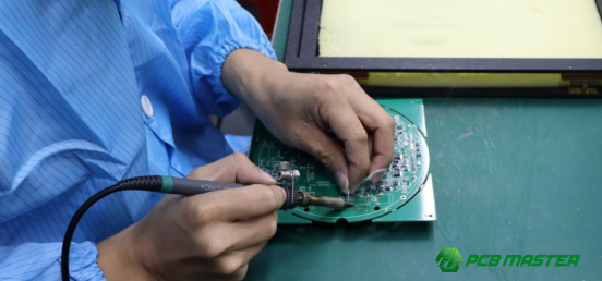
l Manual soldering: Hand-soldered joints are sensitive to pad contamination and soldering technique.
Monitoring each stage helps identify the source of the problem.
What is the defect rate and location pattern of solderability failures?
Solderability failures may occur as batch-wide issues or sporadic defects. Batch-wide failures often indicate a process or material problem, such as contaminated gold surfaces or incorrect soldering profile. Sporadic failures may arise from handling, uneven flux application, or localized pad issues. Common high-risk areas include:
l Large thermal pads, which may not reach sufficient temperature during reflow.
l Fine-pitch pads, where solder bridging or insufficient wetting is more likely.
l Board edges, which can have uneven thermal profiles.
l Specific components prone to contamination or stress during assembly.
Understanding these patterns helps engineers prioritize inspection and corrective actions.
How PCB Factors Cause Immersion Gold Solderability Failures?
PCB factors cause immersion gold solderability failures when issues like incorrect gold or nickel thickness, phosphorus content deviations, black pad formation, surface contamination, oxidation, or poor pad morphology prevent solder from properly wetting and bonding to the pads.
How does gold thickness and quality affect solderability?
The thickness and quality of the gold layer directly influence solder wetting on immersion gold PCBs. The standard thickness is typically ≥0.05 μm, which is enough to protect the nickel layer while allowing solder to bond effectively. If the gold layer is too thick, it may lead to a “black pad” problem, where the nickel beneath corrodes and forms a brittle layer. Measuring gold thickness can be done through cross-section analysis or X-ray fluorescence (XRF) testing to ensure the layer meets specifications and is uniform across all pads. Proper control of gold deposition prevents poor solderability and weak joints.
How do nickel thickness and phosphorus content impact soldering?
Nickel acts as the main barrier layer under gold. Its standard thickness ranges from 3–6 μm, and the phosphorus content should be 7–10%. If the nickel layer is too thin or the phosphorus content is outside the recommended range, the pad may have poor solder wetting, leading to weak or unreliable joints. Analysis is typically performed with cross-section imaging combined with SEM/EDS to verify both thickness and chemical composition. Maintaining correct nickel specifications is critical for soldering reliability.
What is the “black pad” problem and how can it be controlled?
A “black pad” forms when the nickel layer beneath the gold corrodes, creating a phosphorus-rich Ni3P layer. This layer is brittle and prevents proper solder adhesion, causing brittle or cracked joints. Signs include darkened pads, dull or gray solder joints, and easily fractured connections. Detection requires microscopic or cross-section inspection. PCBMASTER recommends strict control of gold plating processes, proper rinsing, and careful storage to prevent black pad formation and ensure consistent solderability.
How do surface contamination and oxidation affect soldering?
PCB surfaces can accumulate organic contaminants such as solder mask residue, fingerprints, or oils, and inorganic contaminants like sulfur compounds or halogen ions. These contaminants interfere with solder wetting and may cause joint defects. Additionally, the nickel layer can oxidize if PCBs are stored improperly in high humidity or high temperature. Maintaining clean storage environments, handling PCBs with gloves, and using proper cleaning methods are key to preventing surface contamination and oxidation, thereby improving solderability.
How do micro-holes, pinholes, and pad surface morphology impact wetting?
Small micro-holes or pinholes in the gold layer expose the underlying nickel, which can oxidize and reduce solder wettability. Similarly, pad surface roughness affects how solder spreads; overly rough or overly smooth surfaces can both create soldering challenges. Other issues include solder mask creeping onto pads or improper pad design, which can lead to uneven solder joints. PCB designers must ensure smooth, uniform pad surfaces, optimized solder mask coverage, and appropriate thermal design to promote proper solder wetting.
How Solder Paste and Assembly Processes Affect Immersion Gold PCB Solderability?
Solder paste quality, flux activity, proper temperature profiles, furnace cleanliness, multiple reflows, and effective cleaning and storage practices all influence immersion gold PCB solderability by affecting how well solder wets and bonds to the pads.
How do solder paste and flux affect solderability?
Solder paste quality and flux directly impact solder wetting on immersion gold PCBs. Expired or low-activity solder paste may not properly flow during reflow, causing incomplete joints or weak adhesion. Flux type, activity, and uniform application also influence wetting; uneven flux can leave areas that resist soldering. PCBMASTER recommends regularly rotating solder paste batches, checking paste activity before use, and optimizing paste printing and stirring procedures to maintain consistent quality. Proper flux and solder paste management ensures reliable solder joints and reduces rework.
How does the reflow or wave soldering temperature profile influence wetting?
Temperature profiles are critical for proper soldering. The peak temperature must reach 230–250°C, and preheat rates and ramp slopes should be controlled to avoid premature flux burnout. Pads with high thermal mass may heat slower, reducing wetting. Using nitrogen-protected reflow atmospheres improves solderability by minimizing oxidation, while air reflow has a narrower process window. Monitoring actual PCB temperatures with thermocouples helps ensure all pads reach sufficient soldering temperature.
How do furnace cleanliness and multiple reflows impact soldering?
A dirty reflow furnace can deposit flux residues or solder particles on the PCB surface, reducing wetting. Multiple reflow cycles can deplete flux activity and accelerate nickel layer oxidation, making pads less solderable. PCBMASTER advises regular furnace cleaning and careful planning of reflow sequences to minimize repeated thermal stress, preserving pad quality and ensuring strong solder joints.
How do cleaning practices and environmental contamination affect soldering?
Residual cleaning agents or improper cleaning can leave films that hinder solder wetting. Environmental contaminants like dust, oils, or moisture also reduce solderability. PCBMASTER recommends using validated cleaning agents, ensuring thorough rinsing, drying PCBs completely, and storing boards in controlled conditions with low humidity. Following strict cleaning and storage protocols helps maintain the solderability of immersion gold PCBs throughout assembly.
How PCBMASTER Systematically Troubleshoots Immersion Gold PCB Solderability Failures?
PCBMASTER systematically troubleshoots immersion gold PCB solderability failures by prioritizing checks for black pads, nickel oxidation, insufficient soldering temperature, surface contamination, solder paste or flux issues, metal layer analysis, soldering atmosphere optimization, and pad or thermal design problems.
What is the priority and method for troubleshooting solderability issues?
PCBMASTER follows a step-by-step, priority-based approach to identify and resolve immersion gold PCB solderability failures efficiently. The process ensures the most critical issues are checked first, allowing engineers to quickly locate the root cause and implement corrective actions.
1. Black pad detection
Black pads occur when the nickel layer corrodes beneath the gold, forming brittle Ni3P. PCBMASTER uses cross-section analysis combined with SEM/EDS to inspect pad structure and composition. Early detection prevents weak or brittle joints from causing reliability failures.
2. Nickel layer oxidation or sulfide formation
Oxidation or sulfur contamination reduces solder wetting. Boards are examined for oxidation or sulfide layers, and baking tests may be performed to distinguish temporary surface issues from permanent metallurgical defects. Storage conditions are reviewed to prevent recurrence.
3. Insufficient soldering temperature
Pads that do not reach adequate temperatures may exhibit poor wetting. Thermocouple measurements on test boards verify that peak temperatures, preheat slopes, and dwell times meet the requirements for large thermal pads and fine-pitch components.
4. Surface contamination testing
Organic and inorganic contaminants can block solder adhesion. PCBMASTER tests pad surfaces by wiping with IPA and re-soldering with fresh solder wire. Improvement indicates contamination as the likely cause.
5. Solder paste or flux replacement tests
If solderability issues persist, new batches of solder paste or flux are tested to rule out material inactivity or uneven flux coverage, which could prevent proper wetting.
6. PCB gold/nickel thickness and phosphorus content analysis
Analytical methods such as XRF and SEM/EDS cross-sections verify that gold thickness, nickel thickness, and phosphorus levels meet specifications, ensuring metallurgical compatibility with solder.
7. Optimization of soldering atmosphere
Using nitrogen-protected reflow can significantly improve wetting compared to air soldering. PCBMASTER evaluates soldering gas conditions and adjusts as needed for sensitive or high-reliability boards.
8. Design issue inspection
Thermal design and pad layout affect solderability. Large pads, uneven thermal mass, or fine-pitch arrangements are reviewed, and adjustments are made to improve uniform heating and solder flow during reflow.
By following this systematic troubleshooting hierarchy, PCBMASTER efficiently isolates the root cause of solderability failures, enabling precise corrective actions and improving overall assembly reliability.
How to Effectively Prevent Immersion Gold PCB Solderability Failures?
Immersion gold PCB solderability failures can be effectively prevented by optimizing pad design and material specifications, controlling storage and surface protection, refining soldering processes, and implementing regular testing and quality monitoring practices.
How can PCB design and material standards prevent solderability issues?
Proper PCB design and material selection are critical to preventing solderability failures. Ensuring adequate pad size and spacing promotes uniform solder flow and reduces the risk of bridging or incomplete joints. Avoiding overly thick gold layers and maintaining compliant nickel thickness (3–6 μm with 7–10% phosphorus) prevents black pad formation and brittle solder joints. By adhering to these design and material standards, PCBs are inherently more solderable, reducing assembly defects and improving long-term reliability.
How does PCB storage and surface protection improve solderability?
PCB storage conditions directly affect surface integrity. Controlling temperature and humidity, using vacuum packaging, and monitoring board expiration dates help prevent oxidation and contamination. Applying protective measures such as anti-oxidation coatings or clean handling practices further ensures that gold and nickel layers remain uncontaminated. Proper storage and surface protection maintain the wetting ability of solder and minimize assembly failures.
How can soldering process optimization reduce solderability problems?
Optimizing the soldering process ensures that solder flows correctly on immersion gold pads. Adjusting temperature profiles to meet the thermal requirements of high-mass pads, maintaining flux activity, and using a nitrogen-protected reflow atmosphere all improve wetting. Careful management of secondary reflows prevents flux exhaustion and nickel oxidation. Process optimization ensures consistent, strong solder joints across the entire PCB.
What practices does PCBMASTER recommend from experience?
PCBMASTER shares practical insights for preventing solderability failures. Selecting high-quality materials from reliable suppliers guarantees gold and nickel layers meet standards. Conducting regular soldering tests and implementing quality monitoring workflows allows early detection of potential defects and maintains consistent assembly reliability. These practices combine design, material control, storage, and process management to minimize soldering issues.
Conclusion
Immersion gold PCB solderability failures result from multiple factors, including PCB design, material quality, storage, and soldering processes. PCBMASTER offers systematic analysis and practical optimization methods to help engineers identify root causes and implement effective solutions. By following these step-by-step recommendations, production teams can improve solder wetting, enhance assembly reliability, and reduce rework, ensuring consistent PCB performance.
FAQs
1. What are the most common causes of immersion gold PCB solderability failures?
The most frequent causes include black pad formation from nickel corrosion, nickel layer oxidation or sulfide contamination, surface contamination, improper solder paste or flux activity, insufficient reflow temperature, and poor PCB design such as uneven pad sizes or spacing.
2. How can black pads be quickly distinguished from ordinary nickel oxidation?
Black pads are typically brittle and appear dark under magnification, often causing solder joints to crack, while ordinary nickel oxidation may form a thin, non-brittle surface layer; cross-section SEM/EDS analysis or baking tests can confirm black pad formation.
3. What should be done if solderability issues persist after replacing solder paste or flux?
If problems remain, check PCB metal layers for gold and nickel thickness, phosphorus content, pad design, storage conditions, and consider reflow atmosphere optimization, as material or process issues may still be affecting wetting.
4. What specific problems can insufficient reflow temperature cause?
Low peak temperatures or uneven heating can prevent solder from fully wetting pads, especially large or high-thermal-mass pads, resulting in partial soldering, weak joints, voids, or solder balling.
5. What solutions exist for solderability failures on large or ground pads?
Solutions include increasing reflow temperature or dwell time, using thermal vias to balance heat, optimizing pad layout, applying more active flux, and verifying sufficient solder paste deposition to ensure complete wetting.

