


PCB Hole to Copper Distance Rules for Reliable and Manufacturable Boards
Every layer of a PCB must be designed with precision, and one critical yet often overlooked detail is the “hole-to-copper” spacing. The hole-to-copper distance refers to the minimum clearance between the walls of a hole and any copper features on the PCB, such as traces, pads, or copper pours. This spacing directly affects the electrical safety, signal integrity, and manufacturability of the board. Too little clearance can lead to short circuits, signal degradation, or production defects, while excessive spacing may waste valuable board space.
So, how should designers determine the proper hole-to-copper distance in actual PCB layouts? With years of experience in delivering high-quality PCBs and PCBAs, PCBMASTER has accumulated extensive expertise in PCB design and manufacturing. Drawing from this experience, PCBMASTER will explain the importance of hole-to-copper spacing and provide practical guidance on how to determine appropriate clearances for different applications—helping ensure your PCB designs are both reliable and manufacturable.
What are the different types of holes and copper features in PCB design?
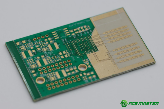
PCB holes and copper features come in several types, each serving a specific purpose in electrical connectivity and mechanical support. Understanding these types is key to designing reliable and manufacturable PCBs.
Hole Classification
1. Through-Holes (PTH: Through, Blind, and Buried Vias)
Through-holes are used to connect electrical signals between different layers of a PCB.
| Via Type | Connection | Visibility | Common Use / Notes |
| Through Via | Passes completely from top layer to bottom layer | Visible on both board surfaces | Used for general layer-to-layer connections |
| Blind Via | Connects an outer layer to one or more inner layers | Visible on only one surface | Common in high-density boards where surface space is limited |
| Buried Via | Connects only inner layers | Not visible from the board surface | Used in multi-layer PCBs to save surface space |
Example: In a 6-layer motherboard, buried vias may connect inner power and ground planes without interfering with signal traces on the top surface.
2. Component Holes
These holes are meant for mounting through-hole components like DIP chips, connectors, or resistors. They are usually plated to provide electrical connectivity.
Example: Installing a 16-pin DIP IC requires 16 evenly spaced component holes.
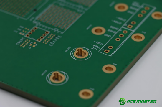
3. Screw or Mounting Holes (NPTH)
Non-plated holes are used for mechanical purposes, such as screws or standoffs. They do not carry electrical current. Designers must leave extra space around these holes to prevent copper damage.
Example: Mounting a metal enclosure to a PCB often requires 4 NPTH holes at the corners with clear copper-free zones around them.
Copper Feature Classification
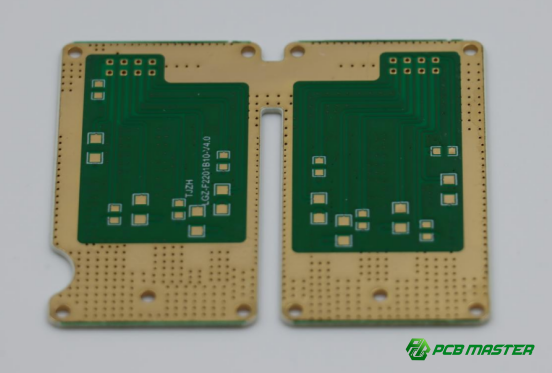
1. Traces (Signal Lines)
Traces are thin copper lines that carry electrical signals between components. Their width and spacing determine current capacity and signal quality.
Example: A 10-mil wide trace may carry low-current signals, while a 30-mil trace might carry power.
2. Pads
Pads are copper areas where components are soldered. They can be through-hole or surface-mount type. Proper pad size ensures a strong solder connection and prevents shorts.
Example: A QFP (Quad Flat Package) IC requires precise pad dimensions to align all pins.
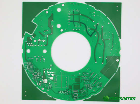
3. Copper Pour / Plane
Large copper areas are used for ground or power planes. They reduce electrical noise and improve thermal performance. Designers often leave holes inside planes (anti-pads) to prevent unintended connections.
Example: A ground plane under high-speed signal traces reduces EMI (Electromagnetic Interference).
4. Board Edge Copper
Copper near the edge of the PCB may be used for shielding, grounding, or heat dissipation. Careful clearance from holes and routing is required to prevent short circuits or board damage during milling.
Example: Edge copper may connect to a metal enclosure for EMI shielding.
Why is hole-to-copper distance critical in electrical PCB design?
Hole-to-copper distance ensures electrical safety, maintains signal integrity, and prevents PCB manufacturing defects. Maintaining proper clearance reduces the risk of shorts, high-voltage breakdowns, and signal issues in complex boards.
Electrical Clearance Requirements
Electrical clearance defines the minimum distance between a hole and surrounding copper to prevent short circuits or breakdowns.
High-voltage circuits require larger hole-to-copper spacing to prevent arcing and ensure compliance with safety standards. Standards like IPC-2221, UL, and IEC provide recommended minimum clearances based on voltage levels. For example, a 100V DC circuit may require 0.2mm (8mil) minimum clearance, while a 1000V DC circuit may need 2–3mm. Designers must check these standards and work with their PCB manufacturer to set appropriate spacing.
Example: In a power supply board handling 500V, increasing the hole-to-copper distance around vias and pads prevents accidental flashover under high humidity or dust conditions.
Creepage Distance and High-Humidity Environments
Creepage distance is the path along the PCB surface between conductive features, which affects insulation in humid or dirty conditions.
Even if the hole-to-copper clearance meets the shortest air distance, moisture on the board surface can create a conductive path. To address this, designers may add slots, grooves, or extra surface spacing around high-voltage holes. This is especially important for outdoor or industrial PCBs exposed to condensation.
Example: On a humid-environment LED driver PCB, small slots are cut between high-voltage vias and surrounding copper to increase creepage distance and reduce leakage risk.
Signal Integrity and Via Design
Hole-to-copper spacing affects how signals travel, especially in high-speed circuits, by controlling parasitic capacitance and reference plane continuity.
l Anti-pad Design: Anti-pads are clearance holes in copper planes around vias to prevent shorting. Adequate anti-pad spacing maintains consistent impedance and reduces noise.
l High-Frequency Effects: If a via is too close to a large copper plane, parasitic capacitance can slow down signals or cause reflections. Proper spacing ensures the signal meets timing and quality requirements.
Example: In a 5G RF PCB, designers leave at least 0.2mm between via barrels and surrounding ground planes to minimize signal distortion and maintain controlled impedance.
How to determine minimum hole-to-copper distance based on PCB manufacturing capability?
The minimum hole-to-copper distance depends on the PCB manufacturer’s process capabilities, including drilling precision, plating limits, and etching tolerances. Proper spacing ensures reliable production, reduces defects, and maintains electrical performance.
Drilling Tolerance and Its Impact on Hole-to-Copper Distance
Drilling tolerance is the potential deviation of a drill during the PCB manufacturing process.
Even precise drilling can shift slightly due to drill vibration or material hardness. If a hole is too close to surrounding copper, this deviation may cause accidental shorts or thinning of copper features. Designers should add a safety margin to account for the drill tolerance.
Example: A drill with ±0.05mm tolerance requires at least 0.2mm spacing from nearby traces on the outer layer to prevent copper damage during drilling. This ensures that slight drill shifts do not compromise electrical integrity.
Via Wall Plating and Etching Limitations
The copper plating on via walls and the etching process for traces affect how close copper can safely be to a hole.
Holes are often plated to create electrical connections. If the copper trace or pad is too close, etching may accidentally remove part of the plating or create shorts. This is especially critical on outer layers, where solder mask and plating tolerances interact.
Example: In a 4-layer PCB, a 0.15mm spacing from plated through-hole walls to the nearest copper trace is often the minimum for reliable manufacturing. Less than this may result in defects during mass production.
Typical Safety Values for Different Processes
Minimum hole-to-copper distances vary depending on layer position and manufacturing precision.
l Outer Layer vs. Inner Layer: Outer layers require slightly more spacing due to additional solder mask and plating processes, while inner layers can tolerate smaller distances.
l Extreme Spacing vs. Cost: Reducing spacing below standard safety values increases production difficulty and cost due to higher precision requirements.
Comparison Table:
| Layer | Typical Minimum Hole-to-Copper Distance | Notes |
| Outer Layer | 0.2mm (8mil) | Includes plating and solder mask margin |
| Inner Layer | 0.15mm (6mil) | Less critical; easier to maintain |
| Extreme Minimum | 0.127mm (5mil) | Requires high-precision process; higher cost |
Example: For a high-density 8-layer PCB, designers may target 0.15mm spacing on inner layers but keep 0.2mm on outer layers to balance cost and manufacturability.
What are the design rules for different types of hole-to-copper distances?
Different hole types require specific minimum distances from copper to ensure electrical safety, manufacturability, and mechanical reliability. Following these rules reduces short circuits, stress damage, and production defects.
Standard Hole-to-Copper Spacing for Through-Holes / PTH
Brief Answer: Through-holes or plated through-holes (PTH) require a standard minimum spacing from surrounding copper features.
A common recommended value is 0.2mm (8mil), which ensures safe manufacturing and reliable electrical connections. The extreme minimum that high-precision processes can achieve is 0.15mm (6mil), though this may increase cost and manufacturing difficulty.
Example: On a 4-layer PCB connecting a microcontroller, maintaining 0.2mm between via walls and nearby traces prevents accidental shorting during drilling and plating.
Minimum Hole-to-Copper Distance for NPTH (Non-Plated Through-Holes)
NPTH, or non-metalized holes, require larger spacing because they have no conductive wall protection.
A safe minimum spacing is ≥0.4mm (16mil) to prevent accidental short circuits. This is especially important in high-voltage circuits or humid environments where moisture could create unintended conductive paths.
Example: Mounting a standoff NPTH in a power supply PCB requires 0.4mm spacing from adjacent traces to avoid arcing or leakage paths.
Screw / Mounting Hole Safety Zone
Mechanical mounting holes must maintain a larger clearance from copper and include a copper-free safety zone.
Recommended spacing is ≥1.0mm (40mil) from the screw edge, plus a reserved copper-free zone around the hole. This prevents mechanical stress from bending or compressing copper traces when screws are tightened.
Example: On a metal-enclosed industrial PCB, mounting holes are surrounded by a 2mm diameter copper-free circle to protect traces from compression or scratches during assembly.
Board Edge Hole to Board Edge Copper Clearance
Holes near the PCB edge need safe spacing from edge copper to prevent damage during milling and copper lifting.
A minimum distance of ≥0.5mm (20mil) is recommended. Proper clearance avoids cutting into hole walls or causing copper to peel off during panel routing.
Example: For a small IoT PCB with edge-mounted connectors, maintaining 0.5mm spacing ensures the board can be routed and the edge copper remains intact.
How can hole-to-copper spacing be optimized in PCB design practice?
Optimizing hole-to-copper spacing involves understanding manufacturer capabilities, setting precise DRC rules, using layer-specific design techniques, and performing DFM checks to prevent production issues and ensure electrical reliability.
Communicate with PCB Manufacturers and Obtain the Latest Process Capability Sheet
The first step in optimizing hole-to-copper spacing is understanding what your PCB manufacturer can reliably produce.
PCB manufacturers provide a process capability sheet that lists minimum drill sizes, plating tolerances, and spacing limits. By reviewing this document, designers can set spacing rules that match real-world production capabilities. Regular communication helps accommodate any updates or changes in the manufacturer’s processes.
Example: A manufacturer may guarantee 0.15mm spacing for inner layers but only 0.2mm for outer layers due to plating and solder mask limitations. Designing within these limits prevents costly redesigns or production failures.
Set PCB Design Software DRC Rules
Design Rule Checks (DRC) in PCB software help enforce proper hole-to-copper spacing automatically.
l Hole to Copper / Hole to Track / Hole to Pad: Ensure that vias and component holes maintain minimum clearance from nearby traces and pads.
l NPTH Hole to Copper / Board Edge to Hole: Set specific rules for non-plated holes and edge clearances to prevent mechanical and electrical issues.
Example: In Altium Designer, a DRC can flag any via closer than 0.2mm to a trace, allowing corrections before production. This reduces errors and ensures manufacturability.
Layer-Specific Spacing and Teardrop Design
Optimizing spacing requires treating inner and outer layers differently and using teardrops to strengthen via-trace connections.
Outer layers typically require more clearance due to solder mask and plating tolerances, while inner layers can tolerate slightly smaller distances. Teardrops are gradual expansions of a trace where it meets a via or pad, reducing the risk of cracking or drill-induced disconnections.
Example: In a 6-layer PCB, inner layer vias may have 0.15mm spacing, while outer layer vias have 0.2mm spacing, with teardrops applied to high-current traces for mechanical stability.
Importance of DFM Checks
DFM (Design for Manufacturability) checks ensure your hole-to-copper spacing meets practical production requirements.
After generating Gerber files, run DFM software or request a pre-production check from your board manufacturer. This step identifies potential spacing violations, weak connections, or interference with mechanical holes before fabrication, saving time and cost.
Example: A high-density IoT PCB with multiple blind vias may fail if anti-pad spacing is too tight. DFM review flags these issues, allowing design adjustments before panel production.
What core principles does PCBMASTER recommend when designing hole-to-copper spacing?
PCBMASTER advises prioritizing reliability, adapting spacing based on hole and copper types, and consulting manufacturers when unsure to ensure safe, manufacturable, and high-quality PCB designs.
Prioritize Reliability by Leaving the Largest Possible Spacing
Whenever space allows, maintain larger hole-to-copper distances to maximize electrical safety and manufacturing reliability.
A larger spacing reduces the risk of shorts, accidental copper etching, or signal interference. It also provides tolerance for drilling deviations and plating inconsistencies. Even if your design could technically fit smaller clearances, prioritizing safety prevents long-term failures and reduces costly rework.
Example: On a 12-layer high-voltage PCB, designers may leave 0.3mm spacing for through-holes instead of the minimum 0.2mm, ensuring extra clearance under high humidity and vibration conditions.
Adjust Safety Distance Based on Hole Type and Copper Type
Not all holes and copper features are equal; spacing should be tailored according to their characteristics.
l Through-holes (PTH): Standard spacing of 0.2mm is usually sufficient, but can be increased for high-current or high-voltage areas.
l NPTH / mounting holes: Require larger spacing (≥0.4mm to copper, ≥1.0mm for screws) due to lack of plating and mechanical stress.
l Copper type: Traces, pads, or planes may have different spacing needs. Large copper pours require slightly more clearance to avoid accidental shorts.
Example: A PCB with both dense signal traces and NPTH standoffs may use 0.2mm spacing for signal vias but 0.5mm around NPTH holes to maintain reliability.
Consult PCB Manufacturers When Uncertain
When spacing rules are unclear or the design is complex, always check with your PCB manufacturer.
Manufacturers can provide process-specific recommendations, minimum clearances, and advice for high-density or high-voltage designs. This prevents costly errors and ensures that designs comply with real-world production capabilities.
Example: For a new multi-layer PCB with mixed PTH and blind vias, contacting the manufacturer revealed that outer layer via-to-plane spacing needed 0.25mm instead of 0.2mm to ensure plating quality, avoiding potential short circuits.
Conclusion
Proper hole-to-copper spacing is key to PCB reliability, manufacturability, and electrical performance. By understanding hole and copper types, applying layer-specific clearances, using DRC and DFM checks, and consulting your manufacturer when needed, designers can prevent shorts, signal issues, and production defects. PCBMASTER’s experience shows that prioritizing safe spacing and following best practices ensures robust, high-performing, and manufacturable PCBs. Careful design today saves time, cost, and potential failures tomorrow, making every board safer and more reliable in real-world applications.
FAQs
Does the minimum hole-to-copper distance vary between different PCB layers?
Yes. Outer layers typically require slightly larger spacing due to solder mask, plating, and exposure to mechanical stress. Inner layers can tolerate smaller distances because they are protected by surrounding layers, but plating tolerances must still be considered. For example, 0.2mm on outer layers vs. 0.15mm on inner layers is common for standard PCB processes.
How does hole-to-copper spacing affect signal integrity on high-speed boards?
Spacing influences parasitic capacitance and impedance. Vias placed too close to large copper planes can create unwanted capacitance, causing signal reflections or timing issues. Proper anti-pad design and uniform spacing help maintain consistent impedance for high-speed traces.
Why do non-plated through-holes (NPTH) require larger hole-to-copper spacing?
NPTH holes lack conductive plating, so nearby copper is more prone to accidental shorts from moisture, dust, or mechanical stress. Increasing spacing (≥0.4mm / 16mil) ensures safety, especially in high-voltage or humid environments.
What are the design restrictions for copper traces near screw or mounting holes?
Avoid routing any critical signals or power traces directly under or too close to screws. Mechanical stress during assembly can crush or break copper, causing short circuits or open connections. Maintain a copper-free safety zone (≥1mm / 40mil) around mounting holes.
How is hole-to-copper spacing calculated for high-voltage PCB designs?
High-voltage spacing depends on working voltage, creepage requirements, and applicable standards (IPC-2221, UL, IEC). Higher voltages require exponentially larger gaps. Designers must consider both direct distance and surface creepage paths, sometimes adding slots or extra isolation to meet safety standards.

