


PCB Gold Surface Treatments Explained: ENIG, ENEPIG, Hard Gold & Soft Gold Applications
Gold surface treatments play a crucial role in ensuring the durability, conductivity, and reliability of printed circuit boards (PCBs), especially in high-performance and high-reliability applications. As the demand for advanced electronic devices grows, selecting the right surface treatment becomes a key factor in achieving optimal performance. Among the various methods, gold plating stands out for its excellent corrosion resistance and superior electrical properties. However, choosing the most suitable gold treatment—whether ENIG, ENEPIG, hard gold, or soft gold—depends on specific application needs, such as solderability, durability, and bonding requirements. Each method offers distinct advantages and limitations, making it essential to understand their differences in order to make an informed decision. This article explores the different types of gold surface treatments used in PCB manufacturing, comparing their features, benefits, and ideal use cases, helping you choose the best option for your project.
What is PCB Gold Surface Treatment?
Definition and Overview
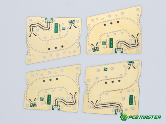
PCB gold surface treatment refers to the process of applying a thin layer of gold to specific areas of a PCB. This treatment is crucial because it enhances the PCB’s performance by improving its electrical conductivity, corrosion resistance, and overall durability. The primary purpose of gold plating in PCBs is to ensure high-quality connections between components and to prevent oxidation, which can affect the longevity and reliability of electronic devices.
Gold surface treatment is commonly used on solder pads, connectors, and other contact points where reliable electrical performance is essential. The gold layer creates a stable, long-lasting surface that prevents wear and tear, ensuring the PCB functions well even in harsh conditions. This is especially important in high-reliability applications such as aerospace, medical devices, and high-end consumer electronics.
Basic Principles and Importance
Gold surface treatment in PCBs is typically achieved through two methods: electroplating (electrolytic) and chemical deposition. The process involves coating copper traces or pads with a thin layer of gold. The chemical method uses a chemical reaction to deposit gold on the copper, while the electroplating method uses an electrical current to deposit gold.
Gold is chosen because of its excellent properties: it is a highly conductive metal, it resists corrosion, and it is non-reactive, which ensures stable connections over time. For PCBs, these properties are critical to maintaining signal integrity and preventing issues like signal degradation or short circuits.
In practical terms, gold surface treatment allows PCBs to handle more heat, resist corrosion from moisture or chemicals, and last longer in environments where other materials might degrade quickly. For example, in consumer electronics, the gold layer ensures that devices continue to function properly for years, even with frequent usage and exposure to varying temperatures and humidity levels.
Types and Classifications of PCB Gold Surface Treatments
The types and classifications of PCB gold surface treatments include electrolytic gold, which is thick and durable for high-wear applications, and chemical gold, which is thin and uniform for finer applications, with hard gold offering enhanced durability for connectors and soft gold providing flexibility for wire bonding and chip packaging.
Electrolytic Gold vs. Chemical Gold: Key Differences
What are Electrolytic and Chemical Gold?
Electrolytic gold and chemical gold are two primary methods of gold surface treatment in PCB manufacturing. The key difference lies in the way gold is deposited onto the PCB surface.
l Electrolytic Gold (also called electroplated gold) uses an electrical current to deposit a gold layer onto a conductive surface, like copper. In this process, gold ions in a solution are reduced onto the surface when an electrical current is passed through the solution. This results in a thick, durable gold layer.
l Chemical Gold (also called electroless gold) is deposited using a chemical reaction rather than electricity. In this method, a chemical bath causes gold to attach to the surface without the need for an external current. The gold layer is thinner and is often used for finer applications where a uniform, smooth finish is important.
Deposition Methods and Their Applications:
l Electrolytic Gold: The process is suitable for areas that require thicker gold coatings, such as connectors and gold fingers (the parts of a PCB that connect with slots or sockets). It is commonly used in applications that require wear resistance and durability.
l Chemical Gold: This method is used for applications where uniformity and thinness are essential, such as fine-pitch soldering or areas where gold’s corrosion resistance is needed, but the thickness doesn’t need to be as high. It’s often used in consumer electronics, automotive, and telecommunications.
Hard Gold vs. Soft Gold: Key Differences
What is Hard Gold?
Hard gold refers to gold that is mixed with other metals like nickel or cobalt to increase its hardness. This alloyed gold is particularly useful in areas that experience frequent mechanical contact and wear, such as gold fingers or test points.
l Hardness and Durability: Hard gold has a higher resistance to wear and tear, making it ideal for applications that involve frequent insertion and removal, like connectors and card slots. These areas require a robust material that maintains its electrical properties even after extensive use.
l Applications: It is commonly used for gold fingers, switch contacts, and test pads in connectors, where durability and low contact resistance are essential.
What is Soft Gold?
Soft gold, in contrast, has a much higher purity level, often 99.9% or higher, and is much softer compared to hard gold. Soft gold is used in applications where flexibility and ease of bonding are essential, particularly in wire bonding and chip packaging.
l Purity and Flexibility: The high purity and softness make it perfect for gold wire bonding in semiconductor packaging, where gold wires need to be attached to delicate semiconductor materials. The soft nature of the gold allows it to deform easily, forming a strong, reliable bond.
l Applications: It is primarily used in chip bonding applications, particularly in ball grid array (BGA) or chip-on-board (COB) packages where gold wire is bonded to the pads of the chip.
Main PCB Gold Surface Treatment Processes and Their Applications
The main PCB gold surface treatment processes include ENIG for cost-effective soldering, ENEPIG for high-reliability applications, electrolytic hard gold for durable connectors, and electrolytic soft gold for wire bonding and chip packaging, each with specific advantages based on their intended use.
ENIG (Electroless Nickel Immersion Gold)
How does ENIG work?
ENIG involves chemically depositing a layer of nickel onto a copper pad, followed by a thin layer of gold. The nickel serves as a barrier to prevent copper from migrating into the gold, while the gold provides a reliable, corrosion-resistant surface for soldering and component connections.
Applications:
ENIG is widely used in consumer electronics, communication devices, and automotive electronics. It is ideal for applications that require reliable soldering and high-quality connections, such as motherboards, smartphones, and automotive control systems.
Pros and Cons:
l Advantages: ENIG offers cost-effectiveness, smooth and even surfaces, and is great for solderability. It is also highly effective in preventing oxidation.
l Disadvantages: ENIG can suffer from the black pad issue, where the nickel layer is over-etched, leading to poor solder joint reliability. This issue can occur if the chemical plating process is not carefully controlled.
ENEPIG (Electroless Nickel Electroless Palladium Immersion Gold)
How does ENEPIG work?
ENEPIG is an upgraded version of ENIG, with an additional layer of palladium between the nickel and gold layers. This extra layer prevents the black pad problem, making it more reliable for high-end applications where solder joints need to be stronger.
Applications:
ENEPIG is commonly used in high-reliability products, such as chip packaging, aerospace, and military applications. It is particularly useful for components that require both gold bonding wire and copper wire bonding, such as BGA (Ball Grid Array) or CSP (Chip Scale Package).
Pros and Cons:
l Advantages: ENEPIG provides excellent soldering and wire bonding capabilities. The palladium layer eliminates the black pad issue and improves the overall durability of the PCB surface.
l Disadvantages: ENEPIG is more expensive and requires a more complex process than ENIG, which can increase production costs.
Electrolytic Hard Gold
How does Electrolytic Hard Gold work?
Electrolytic hard gold is deposited by using an electroplating process, where a gold-nickel or gold-cobalt alloy is plated onto the PCB. This method results in a thicker, harder gold layer compared to other techniques, making it suitable for applications that need greater mechanical strength.
Applications:
Electrolytic hard gold is commonly used for gold fingers, switch contacts, and frequent plug-and-play connectors. These applications are typically found in devices like PCBs for gaming consoles, server boards, and test equipment where frequent insertion and removal are expected.
Pros and Cons:
l Advantages: Hard gold is highly durable, wear-resistant, and maintains low contact resistance. It is perfect for applications where parts experience frequent mechanical stress.
l Disadvantages: It is costly, and the surface is not as smooth as other gold treatments. Also, the thickness of the plating can result in uneven surfaces, which might complicate some delicate soldering processes.
Electrolytic Soft Gold
How does Electrolytic Soft Gold work?
Electrolytic soft gold is applied through the electroplating process, where high-purity gold is deposited onto the PCB surface. This results in a thinner and more malleable gold layer, which is suitable for applications where flexibility and ease of bonding are important.
Applications:
This gold treatment is commonly used in gold wire bonding, chip packaging, and semiconductor applications. It is ideal for high-precision electronics where wire bonds must be made with ease, such as in high-performance semiconductors and microprocessors.
Pros and Cons:
l Advantages: Electrolytic soft gold offers high purity, is easy to press-fit or bond, and provides excellent electrical conductivity. It is perfect for fine-pitch applications and wire bonding.
l Disadvantages: Soft gold is vulnerable to scratches and damage due to its softness. It is also more expensive compared to other treatments, making it less ideal for mass-produced consumer devices.
Comparison Table
Surface Treatment How It Works Applications Advantages Disadvantages ENIG (Electroless Nickel Immersion Gold) Nickel layer is chemically deposited onto copper, followed by a thin gold layer. Nickel prevents copper migration. Consumer electronics, communication devices, automotive electronics. Cost-effective, smooth surface, excellent solderability, prevents oxidation. Can suffer from black pad issue if process control is not ideal. ENEPIG (Electroless Nickel Electroless Palladium Immersion Gold) Adds a layer of palladium between the nickel and gold to prevent black pad issues. High-reliability products, chip packaging, aerospace, military. Eliminates black pad issue, excellent soldering and wire bonding. More expensive, complex process. Electrolytic Hard Gold Gold-nickel or gold-cobalt alloy electroplated for a thick, hard gold layer. Gold fingers, switch contacts, connectors in gaming consoles, servers. Highly durable, wear-resistant, low contact resistance, ideal for mechanical stress. Expensive, uneven surface, not ideal for delicate soldering. Electrolytic Soft Gold High-purity gold electroplated onto the surface, providing a thin, malleable layer. Gold wire bonding, chip packaging, semiconductors. High purity, easy to press-fit or bond, excellent conductivity. Susceptible to scratches, expensive for mass production.
| Surface Treatment | How It Works | Applications | Advantages | Disadvantages |
| ENIG (Electroless Nickel Immersion Gold) | Nickel layer is chemically deposited onto copper, followed by a thin gold layer. Nickel prevents copper migration. | Consumer electronics, communication devices, automotive electronics. | Cost-effective, smooth surface, excellent solderability, prevents oxidation. | Can suffer from black pad issue if process control is not ideal. |
| ENEPIG (Electroless Nickel Electroless Palladium Immersion Gold) | Adds a layer of palladium between the nickel and gold to prevent black pad issues. | High-reliability products, chip packaging, aerospace, military. | Eliminates black pad issue, excellent soldering and wire bonding. | More expensive, complex process. |
| Electrolytic Hard Gold | Gold-nickel or gold-cobalt alloy electroplated for a thick, hard gold layer. | Gold fingers, switch contacts, connectors in gaming consoles, servers. | Highly durable, wear-resistant, low contact resistance, ideal for mechanical stress. | Expensive, uneven surface, not ideal for delicate soldering. |
| Electrolytic Soft Gold | High-purity gold electroplated onto the surface, providing a thin, malleable layer. | Gold wire bonding, chip packaging, semiconductors. | High purity, easy to press-fit or bond, excellent conductivity. | Susceptible to scratches, expensive for mass production. |
How to Choose the Right Gold Surface Treatment for PCBs
To choose the right gold surface treatment for PCBs, select ENIG for soldering, ENEPIG for wire bonding, electrolytic hard gold for connectors and gold fingers, and electrolytic soft gold for chip packaging and gold wire bonding, based on specific application needs.
Choosing Based on Soldering Needs
Which gold surface treatment is best for soldering?
For most soldering applications, ENIG (Electroless Nickel Immersion Gold) is the ideal choice. It provides a smooth, reliable surface that is perfect for soldering components onto the PCB. ENIG’s thin gold layer ensures excellent solderability while also providing corrosion resistance. It is widely used in industries like consumer electronics, telecommunications, and automotive.
How to avoid the black pad issue?
One of the common problems with ENIG is the black pad issue, where improper plating can cause the nickel layer to degrade, leading to poor solder joint quality. To prevent this, ensure that the PCB supplier’s plating process is stable and well-controlled. Regular monitoring of chemical baths and temperature conditions is essential to maintain consistent plating thickness and quality, which helps avoid black pad failures.
Choosing for Gold or Copper Wire Bonding
Which surface treatment is best for wire bonding?
When it comes to gold wire bonding or copper wire bonding, ENEPIG (Electroless Nickel Electroless Palladium Immersion Gold) is the top choice. ENEPIG's added layer of palladium between the nickel and gold layers makes it ideal for both gold-to-gold and copper-to-gold wire bonding. This process ensures stronger bonds and a more reliable connection, making it perfect for applications in semiconductor packaging and high-performance electronics like BGAs (Ball Grid Arrays).
ENEPIG’s versatility makes it a go-to solution for complex wire bonding processes, ensuring high-quality bonds that last, even under thermal cycling and mechanical stress.
Choosing for Gold Fingers and Frequent Plug-in Connectors
What is the best gold treatment for connectors?
For gold fingers and frequent plug-in connectors, electrolytic hard gold is the most suitable option. Hard gold, created by electroplating, is mixed with metals like nickel or cobalt, which increases its hardness and wear resistance. This is crucial for connectors and gold fingers, which experience regular insertions and removals.
Hard gold ensures reliable electrical connections and low contact resistance, even after frequent mechanical cycling. It's widely used in connectors for computer boards, game consoles, and communication equipment.
Choosing for Chip Packaging and Gold Wire Bonding
What surface treatment is best for chip packaging?
For chip packaging and gold wire bonding, electrolytic soft gold is the ideal choice. Soft gold has a high level of purity and is extremely malleable, making it perfect for wire bonding. The soft nature of the gold ensures that gold wires can easily form strong, reliable bonds to the chip pads.
Soft gold is commonly used in semiconductor packaging, especially for high-performance chips like microprocessors and memory modules, where consistent bonding quality is essential. Despite its higher cost, it offers excellent electrical conductivity and is critical in ensuring the long-term reliability of the chip-to-package connection.
Core Technical Differences in PCB Gold Surface Treatments
The core technical differences in PCB gold surface treatments include hard gold's durability for wear-prone applications, soft gold's malleability for wire bonding, electrolytic gold's thick coatings for high-durability needs, chemical gold's smoothness for fine-pitch soldering, and ENEPIG's palladium layer that prevents the black pad issue and ensures reliable soldering.
Physical Differences Between Hard Gold and Soft Gold
What are the key physical differences between hard gold and soft gold?
The primary differences between hard gold and soft gold lie in their hardness, wear resistance, and suitability for different applications.
l Hard Gold: Hard gold is an alloy of gold mixed with other metals like nickel or cobalt, which significantly increases its hardness and wear resistance. This makes it ideal for applications where the PCB will experience frequent mechanical contact, such as connectors, gold fingers, and switch contacts. Hard gold provides a long-lasting, durable connection that resists abrasion and maintains low contact resistance over time.
l Soft Gold: Soft gold is highly pure gold (99.9% or higher), making it softer and more malleable. This softness makes it perfect for wire bonding applications, such as chip packaging or semiconductor packaging, where fine gold wire needs to bond reliably to the PCB. Although soft gold offers excellent electrical conductivity and is great for bonding, it wears out quickly when subjected to mechanical stress or friction.
Advantages and Limitations:
l Hard Gold: The key advantage is its superior durability for applications that require frequent handling. However, it is costlier and may not provide the smooth surface needed for fine wire bonding.
l Soft Gold: Offers excellent conductivity and is essential for chip packaging and gold wire bonding, but it is vulnerable to scratches and damage due to its softness, and it is more expensive.
Technical Differences Between Electrolytic and Chemical Gold
What are the key differences between electrolytic and chemical gold in PCB surface treatments?
The main differences between electrolytic gold and chemical gold are the deposition method, thickness control, and production complexity.
l Electrolytic Gold: Electrolytic gold is applied using an electroplating process, where electricity is used to deposit a gold layer onto a conductive surface. This method allows for the thicker deposition of gold, which makes it suitable for applications that require high wear resistance and mechanical strength, such as gold fingers. However, the plating can sometimes be uneven, making the surface less ideal for fine-pitch soldering or wire bonding.
l Chemical Gold: Chemical gold, also known as electroless gold, uses a chemical reaction to deposit a thin, uniform layer of gold onto the PCB surface without the need for electricity. This method results in a thinner and more consistent gold layer, which is ideal for fine-pitch soldering, sensitive components, and delicate applications. However, it is typically less durable than electrolytic gold, making it unsuitable for applications that require frequent mechanical contact.
Advantages and Limitations:
l Electrolytic Gold: Electrolytic gold offers thicker coatings and is ideal for high-wear applications like connectors and switch contacts. However, it has uneven thickness and requires precise control during the plating process.
l Chemical Gold: Chemical gold provides a smooth and uniform coating and is better suited for fine-pitch soldering and delicate components. However, it is generally thinner and less durable under mechanical stress.
Black Pad Issue and Advantages of ENEPIG
What is the black pad issue, and how can ENEPIG solve it?
The black pad issue occurs when the nickel layer in a chemical gold (ENIG) process becomes over-etched or excessively corroded, leading to the formation of a brittle phosphorus layer. This layer can crack and cause poor solder joint quality, which is detrimental to the long-term reliability of the PCB. The result is a dark discoloration at the solder joint, often referred to as black pad.
How does ENEPIG address this issue?
ENEPIG (Electroless Nickel Electroless Palladium Immersion Gold) addresses the black pad issue by adding an extra palladium layer between the nickel and gold layers. Palladium acts as a barrier that prevents corrosion during the gold plating process. This additional layer improves the reliability of the PCB and ensures that the nickel layer does not degrade or become overly corroded, thus eliminating the risk of the black pad problem.
The Role of Palladium:
The palladium layer in ENEPIG provides an excellent corrosion barrier, ensuring that the nickel and gold layers are preserved throughout the process. It also enhances the solderability of the PCB and provides a reliable surface for wire bonding and chip packaging, making ENEPIG an ideal choice for high-reliability applications such as aerospace and military electronics.
Advantages of ENEPIG:
l Prevents black pad issue by ensuring better corrosion resistance.
l Improves solder joint quality and reliability for fine-pitch components.
l Versatile in supporting both gold-to-gold and copper-to-gold wire bonding.
Conclusion
When choosing the right gold surface treatment for PCBs, it's essential to match the process with the specific needs of the application. Here's a simplified guide for selecting the best surface treatment:
l For general soldering: ENIG (Electroless Nickel Immersion Gold) is the best choice. It provides a cost-effective solution with a smooth, solder-friendly surface.
l For soldering and chip bonding: Choose ENEPIG (Electroless Nickel Electroless Palladium Immersion Gold). This treatment offers strong bond strength and versatility, making it ideal for both gold-to-gold and copper-to-gold wire bonding.
l For gold fingers or connectors with frequent insertions and removals: Electrolytic hard gold is the preferred option. It offers superior durability and wear resistance, ensuring long-lasting connections.
l For chip packaging and gold wire bonding: Electrolytic soft gold is the optimal choice. Its high purity and malleability ensure high-quality bonding, making it perfect for delicate applications.
Selecting the right surface treatment ensures that your PCB meets the specific requirements of your application, enhancing performance and reliability.
At PCBMASTER, we specialize in providing high-quality PCBs and PCBA services. With years of experience, we are dedicated to helping you choose the best surface treatment to optimize your product’s performance, offering expert guidance and top-tier products that meet the highest industry standards.
FAQs
What are the main differences between ENIG and ENEPIG?
ENIG (Electroless Nickel Immersion Gold) and ENEPIG (Electroless Nickel Electroless Palladium Immersion Gold) are both popular gold surface treatments for PCBs, but they have distinct differences. ENIG is a cost-effective solution that involves depositing a thin layer of gold over a nickel barrier layer. While it is widely used for general soldering, it is prone to the black pad issue due to over-etching of the nickel layer.
ENEPIG, on the other hand, adds a palladium layer between the nickel and gold layers, solving the black pad problem and improving reliability. This treatment is ideal for high-reliability applications such as aerospace, military electronics, and advanced semiconductor packaging where both gold-to-gold and copper-to-gold wire bonding are needed. ENEPIG’s ability to enhance bonding strength and prevent corrosion makes it the go-to choice for more demanding applications.
Why is electrolytic soft gold commonly used in chip packaging?
Electrolytic soft gold is preferred for chip packaging and gold wire bonding due to its high purity (usually over 99.9%) and softness. The high purity of soft gold ensures excellent electrical conductivity, which is essential for reliable wire bonding between the gold wires and the PCB pads. The soft, malleable nature of the gold allows it to form strong and durable bonds when subjected to pressure during wire bonding. This makes it particularly suitable for chip packaging, where fine bonding is required, and the risk of mechanical damage from more brittle materials is minimized.
How can the black pad issue in the ENIG process be avoided?
To avoid the black pad issue in the ENIG process, several techniques can be applied:
l Ensure stable process control: Maintaining consistent conditions in the plating bath (such as temperature, chemical concentration, and pH) is crucial. Regular monitoring and adjustments will prevent over-etching of the nickel layer.
l Use high-quality chemicals: Ensure that the nickel bath is fresh and properly maintained, as degraded chemicals can cause uneven plating and increase the risk of black pad formation.
l Optimize plating times: Control the time spent in the nickel and gold baths to prevent over-plating, which can contribute to the creation of the black pad layer.
l Regular maintenance and quality checks: Regularly clean and test the plating equipment to avoid issues related to nickel layer corrosion and improve overall process stability.
By ensuring process consistency and using the correct materials and techniques, the black pad problem can be minimized or even eliminated.
What are the advantages of electrolytic hard gold?
Electrolytic hard gold offers several key advantages, especially for applications that require high durability:
l Superior wear resistance: The addition of other metals like nickel or cobalt in the plating process makes the gold layer much harder than soft gold, offering excellent abrasion resistance.
l Low contact resistance: Hard gold maintains stable electrical connections even under heavy mechanical stress, making it ideal for frequent insertions and removals.
l Application suitability: This type of gold plating is typically used for gold fingers, connectors, and switch contacts, where reliable long-term performance is essential. It’s also ideal for high-frequency and high-durability applications, such as connector pins that endure constant wear.
However, hard gold can be less suitable for fine-pitch soldering or wire bonding, as its surface is rougher compared to softer alternatives.
Why is ENEPIG called the "universal surface treatment"?
ENEPIG is often referred to as the "universal surface treatment" because it offers versatility in supporting multiple bonding techniques:
l Soldering compatibility: The gold layer in ENEPIG allows for excellent soldering, making it suitable for general PCB assembly.
l Wire bonding versatility: ENEPIG supports both gold wire bonding and copper wire bonding, offering high-strength bonds for advanced semiconductor packaging.
l Prevention of black pad issues: By including a palladium layer between the nickel and gold, ENEPIG eliminates the black pad issue, which is a common concern in ENIG processes. This makes ENEPIG more reliable for high-performance, high-reliability applications.
Thanks to these qualities, ENEPIG is the go-to choice for advanced electronics such as BGA (Ball Grid Arrays), CSP (Chip Scale Packages), and ICs, where both soldering and wire bonding are critical. It is considered universally adaptable for modern PCB needs.

