


Understanding PCB Gold Finger Boards: Functions, Types, and Manufacturing Guidelines
The performance of a printed circuit board (PCB) relies heavily on its ability to connect seamlessly with other components. Among the key connectors that ensure this is the gold finger—a small yet crucial part of the board. Gold fingers establish reliable electrical and physical connections with slots like PCIe and memory, facilitating smooth data transfer and power supply. These gold-plated connectors are built to withstand thousands of insertions, but their quality is determined by the precision of their manufacturing process. This article will explore the essential features, production steps, and best practices for ensuring durable and effective gold finger PCBs.
What is a Gold Finger PCB?
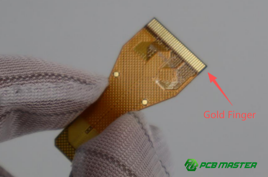
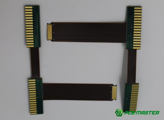
A gold finger is a type of connector on a PCB. It is typically a row of rectangular pads located at the edge of the board, which are coated with a thin layer of gold. These connectors are designed to make electrical and physical contact with corresponding slots or connectors on other boards or devices, such as PCIe slots or memory slots. The gold plating ensures reliable electrical conductivity and long-lasting durability, which is crucial for devices that require frequent insertion and removal, such as graphics cards or network expansion cards.
Function and Application: The Role of Gold Fingers in a PCB
Gold fingers play a vital role in signal transmission and power supply between different parts of a system. When a PCB is inserted into a slot, the gold fingers make contact with metal spring clips inside the slot, creating an electrical connection. This allows data and power to flow smoothly between the boards. Gold fingers are especially common in high-performance devices like servers, graphics cards, and networking equipment, where reliability and performance are critical. Without proper gold finger connections, the system may experience signal loss, poor performance, or even hardware failure.
Origin of the Name: Why is it Called a Gold Finger?
The name "gold finger" comes from the visual appearance of the connector. The gold plating on the contact pads gives them a shiny, finger-like appearance, which is why they are referred to as “fingers.” The term helps distinguish them from other types of PCB connectors that do not have the same appearance or functionality. The gold coating not only enhances their physical appearance but also provides essential properties like high conductivity, resistance to oxidation, and durability—making them ideal for environments where the connectors will be frequently plugged and unplugged.
What Are the Core Functions of a Gold Finger PCB?
The core functions of a gold finger PCB are to provide reliable electrical and physical connections for data transmission, power supply, and secure fixation, while ensuring wear resistance for repeated insertions and removals.
Electrical Connection Function: What is the Role of Signal Transmission and Power Supply?
The gold finger’s primary function is to ensure electrical connections between the PCB and other devices, like expansion cards or motherboards. These connectors provide paths for signal transmission and power supply. When the gold fingers make contact with the corresponding slots, they enable the flow of electrical signals (data) and power between the connected devices. This connection is vital for the proper functioning of the system. For example, in a graphics card, the gold fingers transmit data between the card and the motherboard, while also supplying power to the card. Without a reliable electrical connection, devices can experience performance issues, data loss, or failure to power up.
Physical Connection Function: What is the Role of Slot Clamping Force and Fixation?
In addition to carrying electrical signals, gold fingers also provide physical connections. The clamping force of the slot plays a crucial role in holding the PCB firmly in place. When a device is inserted into a slot, the spring clips inside the slot press against the gold fingers. This pressure not only ensures a solid electrical connection but also helps secure the PCB in place, preventing it from moving or becoming loose during operation. This is important for high-speed data transfer and for preventing physical damage to the board. For example, a PCIe card must stay securely connected to ensure stable data exchange, especially in devices like servers or gaming PCs.
Wear Resistance Requirement: What is the Impact of Repeated Insertion and Removal?
Gold fingers are designed to withstand repeated insertion and removal, a process known as hot-swapping. Every time a card is inserted or removed, the gold fingers experience physical wear. If the connector material isn’t durable enough, it could wear out over time, leading to poor contact, data transfer issues, or complete failure. To prevent this, gold fingers are coated with hard gold, which is known for its high hardness and excellent wear resistance. This allows the connectors to endure thousands of insertions without significant degradation. For example, server expansion cards often undergo frequent plugging and unplugging, so the durability of their gold fingers is essential for long-term performance. Without proper wear resistance, even a small issue could cause a system to malfunction.
What Are the Surface Treatment Methods and Types of Gold Finger PCBs?
The surface treatment methods for gold finger PCBs include hard gold plating for durability, soft gold plating (not suitable for gold fingers due to its softness), and electroless gold plating, with types of gold fingers ranging from conventional (uniform length), step/staggered (varying lengths for hot-swapping), to segmented (multiple sections for different electrical networks).
Gold Finger Surface Treatment Methods
What is Hard Gold Plating? What are its Advantages and Disadvantages?
Hard gold plating is the most commonly used surface treatment for gold fingers. This process involves coating the copper pads with a layer of gold that includes other elements like cobalt to increase hardness. The main advantages of hard gold are its high durability, wear resistance, and excellent electrical conductivity, making it ideal for high-performance applications like graphics cards and network expansion boards. However, hard gold can be more expensive than other coatings due to the complexity of the process. Additionally, it may be slightly less flexible compared to other coatings, which can cause issues in some situations. Despite this, its long-term reliability in high-insertion applications makes it the preferred choice.
Why is Soft Gold Plating Not Suitable for Gold Finger PCBs?
Soft gold is made from high-purity gold and is often used for applications like wire bonding in semiconductor packaging. While it offers excellent electrical conductivity, it is too soft for gold finger PCBs. The softness leads to wear and tear during repeated insertions and removals, which compromises its long-term performance. Unlike hard gold, soft gold cannot withstand the mechanical stress of frequent insertions without degrading, making it unsuitable for connectors that undergo continuous physical contact, like those on expansion cards or memory modules.
What is the Gold Plating Process? What Are Its Surface Characteristics and Limitations?
Gold plating (often referred to as electroless gold) is a method where a thin layer of gold is deposited onto the surface of the PCB. While it results in a smooth surface and provides good electrical conductivity, it has limitations in terms of wear resistance. The gold layer is generally thin and lacks the durability of hard gold plating. As a result, gold-plated fingers are not suited for high-insertion-rate environments. It’s more suitable for low-insertion applications where performance requirements aren’t as high. Gold-plated connectors are typically used in consumer electronics but are not ideal for high-performance computing systems.
Comparison Table of Surface Treatment Methods for Gold Fingers
| Treatment Type | Key Features | Suitable Applications | Limitations |
| Hard Gold | High wear resistance, excellent conductivity | High-usage slots like PCIe, memory cards | Expensive |
| Soft Gold | Excellent conductivity | Chip bonding, wire bonding | Poor wear resistance, not for gold fingers |
| Gold Flashing | Aesthetic appeal, better conductivity | Non-mechanical parts | Thin gold layer, low durability |
Gold Finger Types
What is a Conventional Gold Finger? What is Its Design and Function?
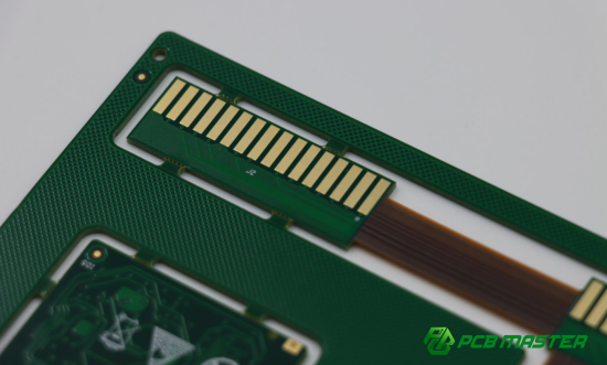
A conventional gold finger features a uniform length of gold-plated pads along the edge of the PCB. This type of gold finger is the most basic and commonly used in most PCBs. It ensures a simple and reliable connection between the board and the corresponding slots. The gold fingers are arranged in a straight line with consistent contact for efficient electrical transmission. These connectors are widely used in devices where the connection doesn’t need to change or vary, such as standard PCI cards or memory expansion modules.
What is a Step or Staggered Gold Finger? What Does It Provide?
A step gold finger, also known as a staggered gold finger, has gold fingers of varying lengths, arranged in a stepped pattern. This design is particularly useful for hot-swappable devices—those that can be inserted or removed without turning off the system. The staggered arrangement allows the connectors to engage or disengage in a specific order, ensuring the correct sequence of electrical connections. This design is often found in high-performance devices such as servers, where you may need to add or replace components while the system is running.
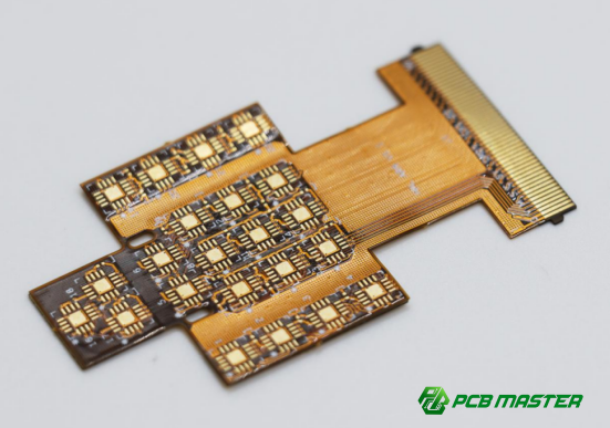
What is a Segmented Gold Finger? How Does it Work?
A segmented gold finger involves dividing the gold finger area into multiple sections, each serving a distinct electrical network. This design is used when the PCB requires different electrical functionalities from the same connector. Segmented gold fingers are often used in complex systems like networking equipment or multi-functional cards where multiple signals must be routed separately. The segmentation provides a more flexible and precise way of connecting various electrical circuits, which is crucial for maintaining system integrity in multi-function applications.
Comparison Table of Gold Finger Types
| Type of Gold Finger | Description | Best For |
| Conventional Gold Finger | Uniform gold-plated pads in a straight line | Standard PCBs, memory modules, PCI cards |
| Step/ Staggered Gold Finger | Varying lengths of gold fingers in a stepped pattern | Hot-swappable devices, high-performance servers |
| Segmented Gold Finger | Multiple gold finger sections for different networks | Multi-functional devices, complex systems like network cards |
What Are the Key Steps in the Production Process of Gold Finger PCBs?
The key steps in the production process of gold finger PCBs include precise engineering design, careful surface treatment and protection, accurate shaping and bevel processing, and thorough testing and inspection to ensure optimal performance and durability.
Engineering Design Stage
What Are the Requirements for Bevel Design? Why Are Angle and Depth Important?
The bevel design refers to the angled edges of the gold fingers. It’s crucial for ensuring proper fit and minimizing stress during insertion and removal. The angle and depth of the bevel directly affect the ease of contact between the gold fingers and the slots they connect to. A typical angle is 20° to 45°, depending on the application. The correct angle helps prevent the fingers from bending or breaking during the insertion process. Similarly, the depth of the bevel ensures that the gold fingers reach deep enough into the slot for a secure connection, but not so deep that they cause damage when being inserted or removed.
What Are the Requirements for Solder Mask Design?
The solder mask design is critical for ensuring that the gold finger area remains clean and free from any solder resist. In the gold finger region, the solder mask must be removed to expose the copper beneath for gold plating. This ensures a proper gold deposition on the fingers. Additionally, the opening for the gold fingers needs to be precise so that the plating process is accurate and consistent. If the solder mask isn’t properly designed, it could lead to uneven plating, affecting the electrical conductivity and wear resistance.
What Are the Requirements for Trace Design and Electroplating Leads?
For gold fingers to be properly electroplated, it’s essential that trace designs are well-planned. Electroplating leads must be designed to ensure that gold is applied uniformly to the fingers. If the lead design is poor, the gold plating might not cover the entire contact area, leading to inconsistent performance. This also means that any electrical signals transmitted through the gold fingers may encounter higher resistance or signal loss. Properly designing the traces and leads ensures that the gold fingers are robust and meet electrical conductivity standards.
Surface Treatment and Protection
What Is the Surface Treatment for Non-Gold Finger Pads?
For pads that are not part of the gold finger area, different surface treatments are used, such as solder mask or immersion gold. These treatments protect the pads from oxidation, contamination, and provide a reliable surface for soldering components. The treatment for non-gold finger pads ensures the entire board remains durable and functional, while the gold fingers receive the necessary electroplating treatment for maximum conductivity and longevity.
What Are the Protection Measures for the Gold Finger Area?
The gold finger area requires specific protection during the manufacturing process. After the gold fingers are plated, they are sensitive to contamination from oils, fingerprints, or debris. To avoid this, manufacturers use protective tape or specialized covers over the gold finger region. This helps maintain the integrity of the gold plating and ensures that the fingers do not get damaged during handling, transport, or storage. Careful attention is needed to protect the gold fingers from scratches or wear that could compromise their performance.
Shaping and Bevel Processing
How Is CNC Milling Used in the Manufacturing Process?
CNC (Computer Numerical Control) milling is used to cut and shape the entire PCB, including the gold finger areas, to precise dimensions. This process involves automated machines that use computer programs to control cutting tools, ensuring consistent and accurate shaping. CNC milling allows manufacturers to create the exact contours and dimensions required for the gold finger connectors. This is especially important for the bevel edges, where accuracy is crucial for ensuring a secure fit with slots.
How Is Specialized Bevel Edge Processing Managed?
Once the PCB is milled, specialized bevel edge machines are used to apply the correct angle to the gold finger edges. These machines ensure that the bevels are uniform and meet the required angle specifications (usually 20° or 45°). Precision is key in this step, as any inconsistencies in the bevel could result in poor contact between the gold fingers and slots. Bevel machines control the cutting depth and angle to prevent any misalignment, which could impact the functionality of the gold fingers.
How Is Burr Control Managed During Production?
After beveling, burrs or small pieces of debris can form along the edges of the gold fingers. These burrs can cause damage to the slots during insertion or affect the signal quality. To prevent this, manufacturers perform a burr removal process, typically using deburring tools or abrasive cleaning methods. Ensuring smooth and clean edges helps preserve the lifespan of the gold fingers and minimizes the risk of damage to both the PCB and the connected devices.
Testing and Inspection
What Is Involved in Visual Inspection of the Gold Fingers?
The visual inspection process is the first step in testing gold fingers. During this step, inspectors check for issues like color uniformity, scratches, or debris on the surface of the gold fingers. The gold fingers should have a bright, even yellow-gold appearance, free from discoloration, fingerprints, or dirt. Any surface imperfections could affect the connector’s performance, so these visual checks are essential in catching potential problems before the board moves to further testing.
What Is Electrical Testing for Gold Fingers?
Electrical testing involves using flying probe testers or fixture-based testing to check if the gold fingers are properly conducting electrical signals. In this process, small probes are placed on the gold fingers to check for continuity and proper signal transfer. These tests ensure that the electrical connections are intact and that the gold fingers are ready for use in a functioning system. Any faults or shorts discovered during this stage are corrected before the board is considered finished.
How Is Thickness Measured for Nickel and Gold Layers?
The thickness of both the nickel and gold layers on the gold fingers is crucial for performance. X-ray measurement tools or other precision equipment are used to check the thickness of both the nickel and gold coatings. Too thin a gold layer can result in poor conductivity and reduced wear resistance, while too thick a layer can cause excess cost or compatibility issues. Ensuring that the gold and nickel layers meet the specified thickness ensures that the gold fingers will function correctly over a long period of time.

What Are the Core Principles in the Manufacturing of Gold Finger PCBs?
The core principles in the manufacturing of gold finger PCBs include ensuring wear resistance with hard gold plating, maintaining cleanliness to avoid contaminants, achieving precision control in bevel angles and solder mask openings, and providing damage-free protection during production, packaging, and transport.
Wear Resistance Requirements: Why Is Hard Gold Electroplating Chosen?
Gold finger PCBs must endure frequent insertions and removals, which is why hard gold electroplating is the preferred choice. Hard gold offers superior wear resistance, which is essential for maintaining the performance of the gold fingers over thousands of cycles. To ensure optimal durability, it is important to control both the thickness and hardness of the gold layer. A thicker gold layer provides better conductivity and longer-lasting durability, while the correct hardness ensures that the fingers can withstand repeated contact without wearing down quickly. Gold fingers with hard gold plating offer the best balance of conductivity and durability, making them suitable for high-usage applications like graphics cards, network cards, and server components.
Cleanliness Requirements: How Do Surface Contaminants Affect Performance, and How Can They Be Avoided?
Maintaining cleanliness is critical during the manufacturing process of gold finger PCBs. Any contaminants such as fingerprints, dust, or oil residues on the gold fingers can negatively impact electrical conductivity and signal transfer. These contaminants can cause poor electrical contact, leading to interference or even complete failure of the connection. To avoid this, strict cleaning protocols are followed throughout production. This includes using protective gloves, dust-free environments, and cleaning solutions to ensure the surface remains pristine. Additionally, protective tape or covers are used to shield the gold fingers from contamination during handling, packaging, and shipping.
Precision Control: Why Is the Accuracy of Bevel Angles and Solder Mask Openings Important?
High precision control is essential for the proper function of gold fingers. The bevel angle (the angled edge of the gold finger) must be carefully calibrated to ensure that it fits perfectly into the corresponding slot. An incorrect bevel angle can lead to improper contact, which can cause poor electrical performance or physical damage to the gold fingers. Similarly, the solder mask openings must be precisely designed so that the gold finger area is free from solder resist. If the opening is too small, the gold plating won’t be applied correctly, leading to inconsistent conductivity. If it’s too large, it can cause plating defects. Therefore, high-precision equipment is used to achieve the exact dimensions and angles required.
Damage-Free Protection Measures: How Are Gold Fingers Protected During Production, Packaging, and Transport?
To prevent damage during production, packaging, or transport, manufacturers take special care to protect the gold finger area. During production, the gold fingers are often covered with protective tape or film to shield them from scratches, abrasions, or oxidation. Additionally, in the packaging phase, the PCBs are placed in foam inserts or bubble wrap to cushion them against physical shocks. For transportation, the boards are securely packed in anti-static bags to prevent static electricity damage. These protection measures ensure that the gold fingers remain in pristine condition, preventing any physical or electrical defects that could affect the overall performance of the PCB.
What Are the Application Areas of Gold Finger PCBs?
Gold finger PCBs are primarily used in PCIe slots and board card slots for high-performance components, as well as in data centers, servers, and telecommunication equipment where reliable, durable electrical connections are critical.
Common Applications: PCIe Slots and Other Board Card Slots
Gold finger PCBs are widely used in PCIe slots and other board card slots. These connectors are crucial for creating reliable electrical connections between expansion cards and the mainboard. For instance, graphics cards, network cards, and storage controllers all use gold finger connectors to transfer data and power effectively. In a PCIe slot, the gold fingers establish a solid connection that allows the card to communicate with the motherboard, ensuring high-speed data transfer and power supply. The durability and low contact resistance provided by gold fingers make them ideal for applications where components are frequently inserted and removed, such as in gaming PCs or workstations.
High-Demand Industries: Data Centers, Servers, and Communication Equipment
Gold finger PCBs are also essential in high-demand industries like data centers, servers, and communication equipment. These sectors rely heavily on reliable, high-performance components that can handle constant operation and large data loads. For example, in data centers, gold finger connectors are used in networking cards, storage arrays, and server expansions where reliability is critical. The high durability and wear resistance of gold fingers ensure that they can handle thousands of insertions without degrading. In telecommunications, devices like routers and switches use gold finger connectors to maintain stable connections for continuous data transmission. The low contact resistance ensures that high-frequency signals pass through without loss, making these connectors indispensable in mission-critical applications where performance cannot be compromised.
Conclusion
Gold finger PCBs are indispensable in ensuring reliable and durable connections across various high-performance applications, from gaming PCs to data centers and telecommunication equipment. Their robust construction, precision design, and exceptional wear resistance make them a vital component in the modern electronics landscape. As the demand for faster, more reliable devices grows, the need for high-quality PCBs becomes even more critical.
This is where PCBMASTER comes in. With years of expertise in PCB and PCBA manufacturing, PCBMASTER is dedicated to providing top-tier products that meet the rigorous standards required in today’s industries. By focusing on precision, durability, and performance, PCBMASTER ensures that every gold finger PCB they produce delivers consistent and reliable results. Whether you're developing complex server systems or high-speed consumer electronics, PCBMASTER is committed to delivering the quality and reliability you need for your projects.
Common Questions and Answers About Gold Finger PCBs
Why Must Gold Fingers Be Electroplated with Hard Gold?
Gold fingers must be electroplated with hard gold because it provides excellent wear resistance, which is essential for connectors that experience frequent insertions and removals. Hard gold offers high durability, low contact resistance, and resistance to oxidation, ensuring reliable electrical conductivity over thousands of cycles. Soft gold, while conductive, is too soft and cannot withstand repeated mechanical stress, leading to potential failure over time.
How Can the Long-Term Stability of Gold Fingers Be Ensured?
The long-term stability of gold fingers can be ensured by using hard gold electroplating with optimal thickness and consistent quality control during manufacturing. Additionally, maintaining a clean environment during production and protecting the gold fingers from contaminants (like oils and fingerprints) is crucial. Regular electrical testing and protective packaging during storage and transport also help to preserve their functionality and performance.
What Is the Impact of Insertion and Removal Cycles on Gold Finger PCBs?
The number of insertion and removal cycles directly impacts the longevity of the gold finger connectors. Over time, repeated contact causes abrasion and wear on the gold layer, potentially leading to increased contact resistance or even complete failure. Proper electroplating thickness, wear-resistant materials, and design optimization can mitigate these effects, ensuring that the gold fingers continue to function reliably for a high number of cycles, typically in the thousands.
What Are the Common Defects Found on Gold Finger Surfaces?
Common defects on gold finger surfaces include scratches, discoloration, fingerprints, and plating inconsistencies like pitting, bubbling, or thinning of the gold layer. These defects can compromise the electrical performance and aesthetic quality of the connectors. Ensuring careful handling, cleaning, and precise plating during manufacturing can prevent these issues.
How Can Damage to Gold Fingers Be Prevented During Manufacturing?
Damage to gold fingers during production can be prevented by implementing protective measures such as protective tape, foam cushioning, or specialized covers. Careful handling with gloves, anti-static environments, and non-abrasive tools is essential. Furthermore, using precision machinery for beveling and milling helps to avoid physical damage during the shaping process, ensuring the gold fingers remain intact and undamaged. Additionally, protective packaging during storage and transport is crucial to avoid physical impact or environmental contamination.
Author Bio
Hi, I'm Carol, the Overseas Marketing Manager at PCBMASTER, where I focus on expanding international markets and researching PCB and PCBA solutions. Since 2020, I've been deeply involved in helping our company collaborate with global clients, addressing their technical and production needs in the PCB and PCBA sectors. Over these years, I've gained extensive experience and developed a deeper understanding of industry trends, challenges, and technological innovations.
Outside of work, I'm passionate about writing and enjoy sharing industry insights, market developments, and practical tips through my blog. I hope my posts can help you better understand the PCB and PCBA industries and maybe even offer some valuable takeaways. Of course, if you have any thoughts or questions, feel free to leave a comment below—I'd love to hear from you and discuss further!

