


Define GND in PCB Design: Why Effective Grounding Matters for Reliable Circuits
Grounding is one of the most fundamental yet often overlooked aspects of PCB design. Without proper grounding, even the most carefully crafted circuits can suffer from noise, instability, and unreliable performance. Whether you're designing a simple device or a high-frequency circuit, the role of ground (GND) cannot be underestimated. It serves as the reference point for electrical potential, ensuring smooth current flow and stable signal integrity. Yet, grounding goes beyond just connecting components; it’s about creating a robust system that minimizes interference, enhances reliability, and prevents costly design failures. This article dives deep into the critical importance of effective grounding in PCB design, exploring why it matters, how to implement it correctly, and the common pitfalls to avoid. By understanding these core principles, you can ensure your circuits perform as expected, even in the most demanding environments.
What Is GND in PCB Design?
GND in PCB design refers to the ground or zero-voltage reference point for the circuit. It acts as the common reference for all the voltages in the system, allowing electrical components to operate with respect to a stable and known reference. When designing a PCB, the ground serves two key functions: first, it ensures that all components have a consistent reference voltage, and second, it provides a path for current to flow back to the power supply after passing through the components.
In simple terms, GND is like the "return road" in a highway system. Electrical current flows out from the power supply to the components (like a car on a highway) and then needs a path back (GND), completing the electrical circuit. Without a ground connection, the circuit can’t work properly, leading to instability, noise, or even failure.
Example:
In a PCB design for a microcontroller circuit, the GND pin connects to the ground, ensuring that all signals are referenced against this zero-voltage point. Without a solid GND, the microcontroller might malfunction because its signals would have no reliable reference.
Types of Grounding in PCB Design
Grounding in PCB design can be done in several ways depending on the complexity of the design and the intended application. Here are the main types of grounding:
1. Single Grounding:
What It Is: This is the simplest form of grounding, where a single reference point is used for the entire circuit. In this setup, all components share the same GND connection.
When to Use It: Single grounding is common in basic PCB designs with minimal components and low-frequency applications, where interference is not a major concern.
Example: A basic LED circuit, where a single ground connection is sufficient.
2. Multi-Grounding:
What It Is: In more complex designs, multiple ground points are used to separate different sections of the PCB. This helps reduce interference, as high-frequency signals won’t interfere with low-frequency ones.
When to Use It: Multi-grounding is typically used in circuits with both analog and digital components, such as audio amplifiers or communication systems.
Example: In a PCB that integrates both digital microprocessors and analog sensors, separate grounds help isolate noise between these two sections.
3. Floating Grounds:
What It Is: Floating grounds are used when no direct electrical connection to the earth is made, which can be common in battery-powered systems or isolated designs.
When to Use It: This type of grounding is useful in sensitive, low-power applications where noise from the earth or external sources needs to be avoided.
Example: A portable medical device where the ground is electrically isolated to prevent interference with delicate sensors.
| Type of Grounding | Description | Use Case |
| Single Grounding | A single reference point for all components. | Simple circuits with low frequency. |
| Multi-Grounding | Multiple ground points for different sections of the circuit. | Complex circuits with both analog and digital components. |
| Floating Grounds | No direct connection to earth; isolated ground. | Low-power, isolated devices like portable sensors. |
How GND Relates to Other Components in a PCB
The GND plane is central to maintaining the stability and reliability of a PCB. Ground planes and power planes work together to ensure that the electrical signals can flow without interference, and the circuit components can function as expected.
1. Relationship Between Power and Ground Planes:
Power Planes provide a stable source of voltage for the PCB components, while ground planes offer a return path for the current. These two planes are often placed parallel to each other, ensuring that the power supply and return paths are as close as possible to minimize noise and voltage fluctuations.
Example: In high-speed digital designs, a solid ground plane under the PCB helps reduce signal integrity issues by providing a stable reference for the signals, ensuring faster and more reliable communication between components.
2. Importance of GND for Signal Integrity and Noise Reduction:
A well-designed GND system is essential for signal integrity, especially in circuits that operate at high frequencies. If the ground path is not optimized, it can lead to ground bounce, where voltage fluctuations in the ground can disrupt the signals, causing errors or noise in the circuit.
Example: In high-speed circuits like RF communication boards, poor GND design could introduce noise, leading to dropped signals or distorted data.
A properly implemented GND system, including solid ground planes and proper routing of return paths, significantly enhances signal quality and reduces electromagnetic interference (EMI), ensuring the PCB functions as intended in real-world conditions.
Why Is Effective Grounding Important in PCB Design?
Effective grounding in PCB design is crucial for ensuring signal integrity, minimizing electromagnetic interference (EMI), and maintaining reliable circuit performance by providing a stable reference and safe current return path.
Impact of Poor Grounding on PCB Performance
Poor grounding in PCB design can lead to several performance issues that affect the overall functionality and reliability of the circuit. The most common problems include noise, signal integrity issues, and malfunctions.
1. Noise: If the ground plane is not properly designed, it can create a noisy environment for sensitive signals. Noise is unwanted electrical interference that can distort or corrupt data transmission. For example, in a digital circuit, a poor ground connection can lead to fluctuating voltage levels, which may cause errors in the transmitted data.
2. Signal Integrity Issues: In high-speed circuits, the ground path is critical for maintaining signal integrity. If there are poor or incomplete ground connections, the return current might not flow as intended, causing signal reflections, distortions, and even signal loss. This can result in data corruption in high-frequency applications such as radio-frequency (RF) systems or microprocessor circuits.
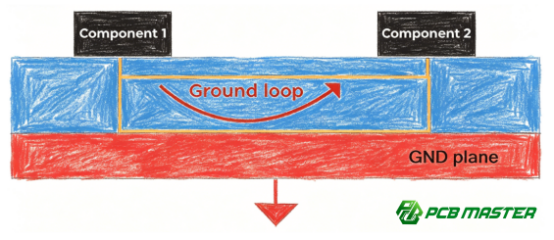
3. Malfunctions: Inadequate grounding can lead to erratic behavior or complete failure of the circuit. In situations where the ground loop is not properly managed, it can cause voltage spikes, which may lead to component damage or system failure.
Example: In a television circuit, improper grounding can cause flickering on the screen or a hum in the audio, both of which are directly related to poor GND design.
Role of GND in Preventing Electromagnetic Interference (EMI)
Grounding plays a significant role in minimizing electromagnetic interference (EMI), which is the unwanted disturbance that can affect the normal operation of electronic devices.
1. How GND Minimizes EMI: A proper ground design helps prevent EMI by ensuring that signals have a stable reference point. This minimizes fluctuations that could generate unwanted electromagnetic fields. In essence, a solid ground plane provides a shield for the circuit, absorbing and dissipating stray interference before it can affect the components.
2. GND's Importance in High-Speed Digital Circuits: In high-speed digital circuits, where signals change rapidly, improper grounding can cause crosstalk (where signals from one circuit interfere with another) and signal degradation. A well-designed GND system ensures that the return current path is short and direct, reducing the possibility of EMI and ensuring that signals remain clean and precise.
Example: In a high-frequency communication system, improper grounding can introduce noise, causing signal dropouts or data errors. A solid ground helps keep the signal clear and minimizes these issues.
Enhancing Circuit Stability and Reliability with Proper Grounding
Effective grounding is essential for maintaining the stability and reliability of a PCB, especially when exposed to varying electrical environments.
1. GND as a Safeguard Against Voltage Fluctuations and Power Surges: A solid ground helps to protect the circuit from voltage fluctuations or power surges by providing a safe return path for excess current. This ensures that the voltage levels remain within the required range for proper component operation. Without this protection, electrical spikes can damage sensitive components, leading to system failures.
2. Grounding Techniques to Maintain Consistent Performance: Certain grounding techniques help keep the performance of a PCB stable under different environmental conditions. For example, ensuring a low impedance ground path and isolating analog and digital grounds can prevent ground loops and reduce the risk of noise affecting sensitive components. This is particularly important in industrial environments, where external factors such as temperature changes and electromagnetic fields can interfere with circuit performance.
Example: In a medical device with precise sensors, poor grounding can lead to false readings or system crashes. A reliable ground design ensures the device functions accurately, even in noisy environments.
By properly designing the ground system, you create a more resilient circuit that can handle external electrical disturbances and continue to perform reliably in a variety of conditions.
How to Implement Effective Grounding in PCB Design?
To implement effective grounding in PCB design, create solid ground planes, minimize ground bounce with short return paths, use decoupling capacitors for noise filtering, and choose the right grounding strategy based on circuit complexity.
Best Practices for Ground Plane Design
What is a solid ground plane and why is it important?
A solid ground plane is a continuous layer of copper on the PCB that acts as a common reference for all components. It provides a stable return path for electrical current, ensuring that signals remain stable and noise is minimized. A continuous, uninterrupted ground plane helps reduce the chances of electrical noise or signal distortion, which is especially critical in high-frequency applications like communication devices.
Benefits of a continuous ground plane:
When the ground plane is uninterrupted, it allows the current to return to the power source without unnecessary detours. This reduces the risk of ground loops and voltage fluctuations, ensuring that signals stay clean and reliable.
Layout considerations:
To create an effective ground plane, the layout must minimize gaps or breaks in the ground layer. One key consideration is avoiding ground loops, which occur when there are multiple paths for current to return to the ground, leading to noise and instability. Careful routing of traces and thoughtful placement of components help maintain an unbroken ground path.
Use of grounding via holes:
Grounding vias (holes) are used to connect the ground plane at different layers of the PCB. These vias help distribute the current more evenly across the board, improving current flow and reducing the chances of voltage spikes or poor signal quality. Proper placement of these vias is crucial for uniform ground distribution.
Minimizing Ground Bounce and Noise in PCBs
What is ground bounce, and why does it occur?
Ground bounce is a phenomenon where fluctuations in the ground voltage disrupt the normal operation of the circuit. It typically happens in high-speed circuits when the return current has to travel a long distance through the ground plane, causing voltage differences that result in signal timing errors or data corruption.
Techniques for minimizing ground bounce:
One effective method is to keep the ground path as short and direct as possible. This can be achieved by careful routing of traces and ensuring that return currents follow the same path as the signal currents. Using multiple ground planes or dedicated return paths can also minimize ground bounce in complex circuits.
Use of decoupling capacitors and resistors:
Decoupling capacitors are placed between power and ground to smooth out fluctuations and provide a stable voltage supply to components. These capacitors help reduce noise by absorbing high-frequency disturbances and filtering them out before they reach sensitive parts of the circuit. Resistors are also used to limit noise and smooth current flow, further stabilizing the signal and minimizing interference.
Example:
In high-speed digital circuits, such as microprocessors, decoupling capacitors help stabilize the power supply and prevent fluctuations that could lead to signal errors or data loss.
Choosing the Right Grounding Strategy for Your PCB
How do you choose between single or multi-ground configurations?
When deciding between single grounding or multi-grounding, consider the complexity and requirements of your PCB design.
Single Grounding is suitable for simpler designs where all components share the same ground reference. It works well for low-speed circuits or designs with minimal power requirements. The single grounding method is cost-effective and easy to implement.
Multi-Grounding is used for more complex designs, such as those with analog and digital components. In this configuration, separate grounds are used for different sections to reduce interference between components that operate at different frequencies. This is important in circuits where analog signals need to be isolated from digital signals to prevent noise.
When to use separate ground planes for analog and digital circuits:
In circuits with both analog and digital sections, it is important to isolate these two parts to minimize crosstalk and prevent digital noise from affecting the analog signals. A separate ground plane for each section can help ensure that each signal type has its own clean, stable reference point.
Example:
In a digital-to-analog converter (DAC) circuit, the analog and digital sections are often grounded separately to prevent high-frequency switching noise from the digital side from interfering with the precise analog signals.
What Are the Common Mistakes in Grounding PCB Designs?
Common mistakes in grounding PCB designs include overlooking ground plane size and layout, neglecting proper ground return paths, and inadequately separating analog and digital grounds, all of which can lead to noise, signal integrity issues, and circuit instability.
Overlooking Ground Plane Size and Layout
What happens if the ground plane is too small or poorly laid out?
A small or fragmented ground plane can cause significant issues in PCB performance. When the ground plane area is insufficient, the current has less space to return efficiently, leading to voltage fluctuations and signal noise. A fragmented ground plane creates multiple ground paths with varying impedance, causing ground loops and potentially disrupting the normal operation of the circuit.
Effects on Signal Quality and Circuit Reliability:
The main issue with insufficient ground plane size and poor layout is the negative impact on signal integrity. In high-speed circuits, poor ground distribution leads to crosstalk between signals, which can cause data errors or slow performance. Additionally, the reliability of the circuit is compromised because the ground plane cannot effectively manage the return currents, leading to instability, especially in sensitive components.
Example:
In a communication circuit, if the ground plane is too small, high-frequency signals may experience distortion or loss of data due to incomplete current return paths.
Ignoring Ground Return Paths
What are ground return paths and why are they important?
A ground return path is the route through which the return current flows back to the power source. Neglecting low-impedance return paths for current can lead to inefficient current flow, which results in voltage differences and noise in the circuit. This can cause components to malfunction or operate erratically.
Consequences of Improper Ground Routing:
Improper routing of the return current can create high impedance paths and increase the chance of ground bounce—a phenomenon where fluctuations in ground voltage cause timing errors or disrupt data transmission. Additionally, improper return paths allow electromagnetic interference (EMI) to creep into the circuit, affecting its performance.
Example:
In high-speed digital systems like microprocessors, improper grounding can lead to signal timing errors or loss of data integrity because the return current doesn't flow efficiently, affecting the overall system reliability.
Inadequate Separation of Analog and Digital Grounds
Why should analog and digital grounds be separated?
When analog and digital grounds share the same plane, the high-frequency noise from the digital side can interfere with the sensitive analog signals, leading to crosstalk and signal distortion. Analog circuits, which require low-noise environments for precise measurements or control, are particularly vulnerable to noise from digital circuits.
Mitigating Noise Through Separation:
To prevent interference, it’s important to use separate ground planes for analog and digital circuits. This ensures that the high-frequency noise from the digital components doesn't affect the analog side. In some designs, the analog and digital grounds can be connected at a single point (known as a "star grounding" method) to minimize noise transfer.
Example:
In a digital-to-analog converter (DAC), if both analog and digital circuits share the same ground, noise from the digital side can cause the analog output to become unstable or inaccurate. By separating the grounds, the DAC output will remain stable and precise.
How Can Grounding Influence PCB Design in High-Frequency Applications?
Grounding in high-frequency PCB designs ensures signal integrity by minimizing loop areas, reducing inductance, preventing ground loops, and isolating noise, which is crucial for maintaining stable, high-performance operation in high-speed and RF circuits.
High-Speed Circuit Considerations for GND
What role does GND play in high-speed PCB designs?
In high-speed PCB designs, grounding is crucial for maintaining signal integrity. High-speed circuits, such as those used in digital communication systems or microprocessors, deal with signals that change rapidly. A stable ground plane ensures that the return current for these signals flows efficiently and without interference, preventing signal distortion or data errors.
Techniques for effective grounding at high frequencies:
At high frequencies, minimizing loop areas and reducing inductance are key to effective grounding. This means keeping the paths that carry the return currents as short and direct as possible. The longer the path, the more inductance it introduces, which can cause the ground voltage to fluctuate and disrupt the signal.
Minimizing loop areas: To reduce the loop area, keep traces close together, ideally within the same plane, to minimize the chance of signal degradation or noise pickup.
Reducing inductance: Use thicker ground planes and vias to ensure a low-impedance path for high-frequency currents, reducing the inductive reactance that can cause voltage drops and signal delays.
Example:
In a high-speed processor circuit, if the ground paths are not properly managed, the return current may cause signal reflections, leading to timing errors or data corruption. A well-designed ground plane ensures clean, stable signal transmission without such issues.
Grounding Challenges in RF Circuits
What are the special grounding needs for RF circuits?
In RF (Radio Frequency) circuits, grounding is particularly critical due to the high-frequency signals involved. At RF frequencies, even small grounding issues can lead to signal distortion, interference, and reduced performance. The key challenge is to ensure that the ground system doesn't introduce additional noise or signal losses that could affect the quality of the RF signal.
Design considerations for RF circuits:
Ground Loops: These occur when there are multiple ground connections that create unwanted current paths, leading to noise and instability. Proper grounding techniques like star grounding help isolate sensitive components from noisy paths.
Isolation: In RF circuits, it’s important to isolate sensitive analog components from noisy digital ones. This is often achieved by using separate ground planes for analog and digital circuits, ensuring that noise from digital signals does not affect analog components.
Shielding: RF circuits are often shielded to prevent electromagnetic interference (EMI) from external sources. The shielding needs to be properly grounded to provide an effective barrier to external noise and prevent ground loop issues.
Example:
In a wireless communication device, improper grounding or shielding can lead to signal attenuation, where the strength of the RF signal is reduced. This could lead to weak or dropped signals, making the device unreliable. Proper ground isolation and shielding techniques ensure strong, clear communication.
How Do Grounding Techniques Affect PCB Testing and Troubleshooting?
Grounding techniques affect PCB testing and troubleshooting by ensuring proper ground continuity, minimizing impedance issues, and helping to identify noise, ground loops, and signal integrity problems that can disrupt circuit performance.
Testing Ground Integrity
How do you test the integrity of a PCB’s ground system?
Testing the ground integrity of a PCB is essential to ensure that the ground connections are continuous, stable, and functioning as intended. Poor grounding can cause signal issues, noise, and system malfunctions. Here are the main methods and tools used for testing ground integrity:
Testing Ground Continuity:
Continuity testing checks whether the ground paths are uninterrupted. Using a multimeter set to continuity mode, you can test between various ground points on the PCB to ensure they are properly connected. A continuous beep from the multimeter indicates a good connection.
Impedance Testing:
Impedance testing is used to measure the resistance of the ground path to AC signals. If the impedance is too high, it could indicate poor ground connections, which could lead to signal distortion or loss. Time-domain reflectometry (TDR) is one common method for measuring impedance in high-frequency circuits.
Tools and Equipment:
Oscilloscopes: Used to observe voltage fluctuations in the ground plane. A noisy or unstable ground will show up as irregular oscillations.
Network Analyzers: These are used in RF designs to measure the integrity of high-frequency signals and check for any grounding issues that affect signal quality.
Example:
In a high-speed digital circuit, using a multimeter for continuity testing and an oscilloscope to check for voltage fluctuations on the ground plane can help pinpoint issues before they affect performance.
Troubleshooting Ground-Related Issues
How do you identify and resolve grounding issues in PCBs?
Ground-related issues can cause various performance problems in PCBs, such as noise, instability, and malfunctioning components. Here’s a step-by-step guide to identifying and resolving these issues:
l Step 1: Check for Ground Continuity
First, ensure that all ground connections are continuous. Use a multimeter to test each ground pin and trace for continuity. If any part of the ground network is broken, it needs to be reconnected.
l Step 2: Measure Impedance
Next, check the impedance of the ground path, especially in high-speed designs. High impedance can lead to signal degradation, so it’s essential to measure and verify that the impedance is within acceptable limits.
l Step 3: Inspect Ground Plane and Traces
Examine the ground plane and its traces. Look for gaps or fractures in the copper, which could cause incomplete return paths for current. Any issues with the ground plane should be addressed by rerouting traces or reinforcing the ground plane.
l Step 4: Check for Ground Loops
Ground loops occur when there are multiple ground paths with different potentials, creating noise and instability. Use an oscilloscope to check for high-frequency noise on the ground, which may indicate a ground loop. If identified, eliminate it by improving the grounding layout or isolating the ground paths.
l Step 5: Test for Noise and EMI
Use an EMI analyzer to check if there’s unwanted electromagnetic interference. Grounding issues can often be the source of EMI, so make sure the ground plane is continuous and isolated from high-frequency signals.
Common Symptoms of Grounding Problems:
l Signal Integrity Issues: Distorted or lost signals are common when the ground path is poor.
l Erratic Behavior: Random resets or component malfunctions often point to grounding problems.
l Increased Noise: Elevated noise levels in the system, especially in analog components, often suggest poor grounding.
Example:
In a communication system, if there’s noise in the transmitted signal, you might identify grounding issues by testing for continuity, measuring impedance, and checking for ground loops. Solving the grounding problem would restore signal clarity and stability.
Conclusion
Effective grounding is a cornerstone of reliable and high-performance PCB design. A well-designed ground system ensures that electrical signals maintain their integrity, minimizes noise, and stabilizes the circuit by providing a safe and efficient return path for current. Whether you're working on high-speed circuits or RF designs, grounding plays a critical role in preventing signal degradation, reducing electromagnetic interference, and ensuring the circuit operates as intended.
By following best practices—such as using solid ground planes, minimizing loop areas, and separating analog and digital grounds—you can avoid common grounding mistakes like poor ground distribution, ground loops, and inadequate return paths. These simple yet vital steps lead to more reliable and efficient PCB designs that can withstand the demands of modern applications.
At PCBMASTER, we understand the importance of effective grounding and its impact on the overall performance of your PCB. As a leading PCB and PCBA supplier, we are committed to providing high-quality products that meet the highest industry standards, ensuring your designs function flawlessly and reliably. With our expertise and advanced manufacturing techniques, we help bring your ideas to life, ensuring both performance and durability in every board we produce.
FAQs
1. What is the difference between ground and power in a PCB?
Ground and power serve two distinct but essential roles in PCB design.
l Ground is the reference point for all voltage levels within the circuit. It is often called "GND" and acts as a common return path for current. All components use ground as a reference for their voltage levels, and it is where current returns after traveling through the components.
l Power (often labeled as VCC or VDD) delivers the energy that components need to operate. It supplies voltage to power the components and drives the current through the circuit, which is essential for the functioning of active components such as microprocessors, sensors, and LEDs.
In simpler terms, ground is the reference point (often zero volts), while power delivers energy to make the circuit work. Without a stable ground, the power supplied would have no reference point, and the circuit would not function correctly.
2. How do I prevent ground loops in my PCB design?
Ground loops occur when multiple paths to ground create different potential differences, which can result in unwanted noise, hum, or instability in the circuit. Here are some practical ways to prevent them in PCB design:
l Star Grounding Configuration:
One of the most effective ways to prevent ground loops is to use a star grounding configuration. This involves connecting all ground points to a single central point, minimizing multiple paths and ensuring that current only returns via one route. This eliminates the possibility of ground loops caused by different potential differences in various parts of the ground network.
l Careful Layout Planning:
Careful routing of ground traces is also important. Ensure that all return currents take the shortest path to the ground. Avoid running traces for sensitive signals close to the ground plane, as this can cause unintended coupling. It's also important to minimize the impedance of the ground path by using wider traces or adding vias to ensure current flows smoothly back to the ground.
l Use Separate Ground Planes:
For complex designs, consider separating the analog and digital grounds, especially in circuits that may produce high-frequency noise. Connect the two grounds at a single point to prevent the noise from propagating into the analog signals.
3. Why is a solid ground plane necessary for high-speed circuits?
A solid ground plane is crucial for high-speed circuits for several reasons:
l Reducing Noise:
A solid, uninterrupted ground plane provides a stable return path for current. When the ground path is solid, noise from external sources or high-frequency signals can be absorbed more effectively, reducing the potential for electromagnetic interference (EMI).
l Stable Signal Returns:
High-speed signals require stable signal returns for proper functioning. A continuous ground plane ensures that return currents flow directly beneath the signal traces, minimizing the risk of signal distortion, reflections, or losses. Without a solid ground plane, high-speed signals can experience timing errors and data corruption.
l Minimizing EMI:
In high-speed circuits, the frequency of signals can be so high that even small variations in the ground path can cause significant noise. A solid ground plane acts as a shield that isolates components and reduces EMI, ensuring better signal integrity and more reliable performance.
4. Can I share a ground plane for analog and digital circuits?
Sharing a ground plane for analog and digital circuits can be done, but it comes with both advantages and disadvantages.
Pros of Sharing a Ground Plane:
l Cost-effective: Using a single ground plane can save space and reduce the complexity of the PCB layout, which is particularly beneficial for simpler designs.
l Simplified Routing: With a shared ground plane, signal traces and power traces are more easily routed, simplifying the overall design.
Cons of Sharing a Ground Plane:
l Noise Coupling: Digital circuits often generate high-frequency noise, which can interfere with sensitive analog signals. If the ground plane is shared, noise from the digital side can couple into the analog signals, leading to signal distortion or crosstalk.
l Ground Loops: Sharing the ground plane without careful design could lead to ground loops, which might increase the noise level and reduce the performance of analog components.
When to Separate the Grounds:
For high-precision analog designs, it is often best to separate the ground planes for analog and digital sections. This can be achieved by using separate ground planes for each, but ensuring they are connected at a single point (usually at the power supply) to maintain a common reference while avoiding noise transfer between the two circuits.
5. How can I improve grounding in my PCB without increasing the size?
Improving grounding in your PCB without increasing its size can be challenging, but it's possible with careful design decisions:
l Optimize Ground Path Layout:
The key to improving grounding without increasing the size is optimizing the layout. Ensure that the ground paths are as short and direct as possible. Use wide traces for ground paths to reduce the resistance and impedance, ensuring a low-impedance return path for current.
l Use Ground Vias Efficiently:
Adding vias to connect ground planes in multi-layer PCBs can help distribute the ground current more evenly across the board. Place vias strategically to ensure a low-impedance path without adding significant board area.
l Use Ground Pour:
Consider using a ground pour (a large copper area dedicated to ground) on layers that don’t have signal traces. This can improve grounding and reduce noise without increasing the PCB size. Ensure the ground pour is continuous to avoid gaps or interruptions in the ground path.
l Minimize Layer Count:
If your PCB design allows, try to use fewer layers. This will help to keep the ground plane intact and prevent the need for additional ground routing or larger areas to handle high-frequency currents.
By following these tips, you can improve grounding while still maintaining a compact design, ensuring your PCB performs efficiently without unnecessary size increases.
Author Bio
Hi, I'm Carol, the Overseas Marketing Manager at PCBMASTER, where I focus on expanding international markets and researching PCB and PCBA solutions. Since 2020, I've been deeply involved in helping our company collaborate with global clients, addressing their technical and production needs in the PCB and PCBA sectors. Over these years, I've gained extensive experience and developed a deeper understanding of industry trends, challenges, and technological innovations.
Outside of work, I'm passionate about writing and enjoy sharing industry insights, market developments, and practical tips through my blog. I hope my posts can help you better understand the PCB and PCBA industries and maybe even offer some valuable takeaways. Of course, if you have any thoughts or questions, feel free to leave a comment below—I'd love to hear from you and discuss further!

