


PCB Edge Plating: Features, Applications, and Why It Matters
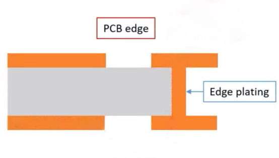
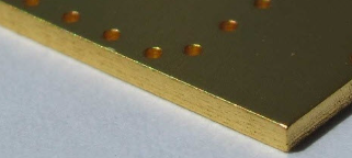
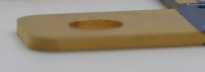
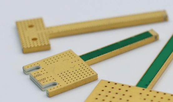
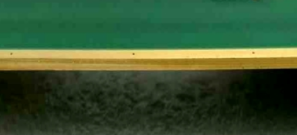
PCB edge plating is a process where a metal layer is applied to the vertical edges of a printed circuit board (PCB). This technique is essential for enhancing both the mechanical strength and electrical conductivity of the PCB. Edge plating ensures that the exposed edges, which are often vulnerable to wear, corrosion, and damage, are reinforced with a durable and reliable metal coating. This provides added protection against environmental factors and improves the overall lifespan of the board.
In electronics, edge plating plays a critical role in ensuring stable connections and maintaining the performance of high-speed circuits. It also helps in improving the quality of electrical signals by reducing resistance and ensuring that currents can flow smoothly across the PCB’s edges. As electronics continue to shrink in size while demanding more power, the importance of edge plating has grown significantly. It is now widely used in various industries such as automotive, aerospace, and medical devices, where reliability and durability are crucial. By improving performance and protecting the integrity of PCBs, edge plating is an indispensable technique in modern electronics manufacturing.
What Are the Key Features of PCB Edge Plating?
PCB edge plating is a vital technique that enhances both the electrical and mechanical properties of a PCB. By applying a metal coating to the edges of the PCB, edge plating improves durability, protects against environmental damage, and ensures stable electrical connections. This process plays a key role in high-performance and high-reliability applications, offering advantages like better conductivity, corrosion resistance, and improved signal integrity.
Materials Used in PCB Edge Plating
Common materials for edge plating (e.g., copper, gold, nickel).
The most commonly used materials for PCB edge plating are copper, gold, and nickel. Copper is the most popular choice due to its excellent electrical conductivity, making it ideal for efficient signal transmission. Gold, while more expensive, is used for its corrosion resistance and ability to maintain low contact resistance, which is especially useful for high-frequency applications. Nickel is commonly used in environments where mechanical strength and wear resistance are important, as it can withstand harsh conditions without corroding.
Material properties that enhance PCB performance.
Each material brings its own unique set of benefits:
l Copper enhances electrical performance, providing high conductivity with minimal resistance, which is essential in power-heavy or high-speed circuits.
l Gold ensures long-lasting connections with minimal signal degradation, especially in applications that require high reliability.
l Nickel improves the physical durability of the PCB, protecting it against wear and tear, making it ideal for industrial or automotive applications where mechanical stress is common.
These materials are chosen based on the specific needs of the PCB’s application, whether it’s improving signal quality, mechanical strength, or environmental protection.
Process of PCB Edge Plating
Step-by-step overview of the plating process.
The PCB edge plating process involves several key steps:
l Surface Preparation: The edges of the PCB are cleaned to remove any dirt, grease, or oxidation, ensuring proper adhesion of the metal coating.
l Plating: The PCB is immersed in a plating solution, which contains metal ions (such as copper, nickel, or gold). Through an electrochemical process, these ions are deposited onto the edges of the PCB.
l Post-plating Treatment: After plating, the board is rinsed and dried. Any excess metal is removed, and the coating is inspected for uniformity and quality.
Types of plating methods: electroless plating vs. electroplating.
There are two main methods used for edge plating:
l Electroless plating: This is a chemical process that does not require electrical current. Metal is deposited uniformly across the edges of the PCB through a chemical reaction, ideal for areas that are difficult to plate.
l Electroplating: This method uses an electrical current to drive the plating process. It produces a thicker and stronger metal coating, making it ideal for high-durability applications. Electroplating is commonly used for edge plating when a thicker layer is needed for mechanical or electrical purposes.
Special considerations for edge plating vs. traditional surface plating.
Unlike surface plating, which focuses on the flat areas of the PCB, edge plating requires more precise control to ensure a uniform coating on the vertical edges. The edges may have irregularities, which makes it essential to pay close attention to the preparation process. Additionally, edge plating may require specific thickness to provide adequate protection and performance, which differs from the even surface plating found on the board’s flat layers.
Thickness and Quality of Plating
How plating thickness is determined.
The thickness of the plating is crucial for both electrical and mechanical performance. It is determined based on the specific needs of the PCB’s application. For instance, high-power or high-frequency circuits may require a thicker layer of plating to ensure proper conductivity and signal integrity. The thickness is usually measured in microns and can be controlled during the plating process by adjusting factors like time, temperature, and plating solution concentration.
Impact of plating quality on PCB performance and durability.
High-quality edge plating enhances the durability and electrical conductivity of the PCB. A well-applied, uniform plating layer ensures low resistance, which is essential for high-speed or high-power applications. On the other hand, poor-quality plating can lead to uneven conductivity, corrosion, and wear, potentially causing PCB failure over time. The quality of the plating directly affects the overall reliability of the device, making it essential for products that require longevity and consistent performance.
Edge Plating vs. Through-Hole Plating
Key differences between edge plating and through-hole plating.
Edge plating and through-hole plating are both used to improve the electrical performance and reliability of a PCB, but they serve different purposes:
l Edge plating applies metal to the edges of the PCB, creating conductive paths for external connections and providing mechanical reinforcement.
l Through-hole plating involves coating the inside of the holes drilled through the PCB, creating connections between layers within the board itself.
Edge plating is primarily focused on external connections and protecting the exposed edges of the PCB, whereas through-hole plating is used for internal layer connections that enable multi-layer boards to function properly.
How edge plating affects electrical performance compared to through-holes.
While both types of plating enhance PCB performance, they affect electrical performance in different ways:
l Edge plating ensures that the electrical signals passing along the edges of the PCB have a low-resistance path, crucial for high-frequency or high-power signals. It can also reduce signal loss and improve overall signal integrity at the edges.
l Through-hole plating, on the other hand, is vital for ensuring the connection between layers of the PCB, allowing signals or power to pass from one layer to another.
Edge plating is especially beneficial in situations where the PCB needs to handle external connections or mechanical stress, while through-hole plating is essential for internal circuit functionality and inter-layer communication.
How Does PCB Edge Plating Enhance PCB Performance?
PCB edge plating significantly enhances the performance of a PCB by improving its mechanical strength, electrical conductivity, and resistance to environmental factors. By applying a metal layer to the edges of the PCB, edge plating ensures better durability, more reliable electrical connections, and greater protection against wear, corrosion, and extreme conditions. These improvements are essential for high-performance applications, extending the lifespan and reliability of the PCB in demanding environments.
Improved Mechanical Strength and Durability
Role of edge plating in reinforcing PCB structure.
Edge plating plays a crucial role in reinforcing the mechanical structure of a PCB. The edges of a PCB are often exposed and vulnerable to damage, especially in high-stress environments. The metal coating applied during edge plating strengthens these edges, making the board more resistant to physical wear and tear. This added strength helps prevent damage during handling, assembly, and operation, ensuring that the PCB maintains its integrity over time.
Resistance to wear, corrosion, and thermal damage.
One of the key benefits of edge plating is its ability to provide resistance to environmental factors like corrosion, wear, and thermal damage. Materials like nickel or gold, commonly used for edge plating, form a protective layer that shields the PCB from moisture, harsh chemicals, and extreme temperatures. This is especially important in industries like automotive or aerospace, where PCBs need to operate in demanding conditions. The edge plating also helps maintain the PCB’s performance, even under mechanical stress or exposure to high temperatures.
Enhanced Electrical Conductivity
How edge plating improves the flow of electrical signals.
Edge plating significantly improves the flow of electrical signals by providing a low-resistance pathway at the edges of the PCB. The metal layer ensures that signals traveling along the edge can pass through without degradation, which is particularly important in high-speed or power-intensive applications. A high-quality edge plating ensures that electrical currents flow smoothly, reducing the risk of signal loss or interference.
Importance for high-frequency applications and low resistance paths.
In high-frequency applications, such as radio frequency (RF) or high-speed digital circuits, edge plating ensures that the electrical signals are transmitted with minimal resistance and interference. The edges of a PCB can act as a key point for high-frequency signals, and the metal coating ensures these signals remain clear and accurate. Additionally, edge plating helps reduce resistive losses by providing a more reliable and stable path for current, which is essential for minimizing heat generation and maximizing power efficiency.
Protection Against Environmental Factors
How edge plating provides insulation and moisture resistance.
Edge plating provides a protective layer that acts as insulation, preventing moisture, dust, and other contaminants from affecting the PCB’s electrical connections. The metal coating, especially when combined with materials like nickel or gold, helps prevent oxidation and corrosion that could occur if the PCB edges were exposed to air or moisture. This is particularly important for outdoor or marine applications where PCBs are exposed to harsh conditions.
Role of edge plating in extending the lifespan of PCBs in harsh environments.
By providing added protection against environmental stress, edge plating significantly extends the lifespan of a PCB. In industrial or automotive settings, where PCBs are exposed to vibration, chemicals, or extreme temperatures, edge plating helps ensure the board continues to function effectively over time. The protective metal layer prevents degradation of the edges, ensuring reliable performance even in harsh environments. This durability makes edge plating a critical feature in ensuring the long-term reliability and performance of PCBs in demanding industries.

What Are the Primary Applications of PCB Edge Plating?
PCB edge plating is widely used across various industries to enhance the performance, durability, and reliability of PCBs. From high-performance electronics like aerospace and medical devices to everyday consumer products, automotive systems, and military technologies, edge plating ensures that PCBs can withstand demanding conditions. It improves electrical conductivity, protects against environmental factors, and strengthens mechanical integrity, making it a crucial feature in many advanced applications.
Use in High-Performance Electronics
Examples: Use of edge plating in aerospace, medical devices, and communications equipment.
PCB edge plating is crucial in high-performance electronics, especially in industries like aerospace, medical devices, and communication systems. In aerospace, PCBs are used in systems like flight control and navigation, where reliability is critical. Medical devices, such as imaging equipment or pacemakers, require PCBs that are both durable and precise, making edge plating essential for maintaining performance over time. Similarly, communications equipment, like antennas and satellite systems, rely on edge plating for stable signal transmission and long-lasting functionality.
Importance for reliability and longevity in demanding applications.
In these high-demand sectors, edge plating is vital for ensuring that the PCB can withstand the stresses of extreme environments, such as temperature fluctuations, vibration, and electromagnetic interference. It helps maintain the integrity and performance of the circuit board, ensuring devices operate reliably and last longer, even under challenging conditions. This durability is particularly important for safety-critical applications like medical equipment or flight systems.
Edge Plating in Consumer Electronics
Common consumer products that benefit from edge plating (e.g., smartphones, laptops).
Edge plating is increasingly used in consumer electronics, particularly in devices such as smartphones, laptops, tablets, and wearable technology. These products often feature complex and compact designs, where every component must work seamlessly to ensure functionality. Edge plating helps enhance the performance and durability of the PCB within these devices, making it crucial for their success.
How edge plating improves signal integrity and device performance.
In consumer electronics, edge plating ensures better signal integrity by providing low-resistance paths for electrical currents and reducing signal degradation at the edges of the PCB. This is particularly important for high-speed applications such as touchscreen responsiveness, Wi-Fi connections, and Bluetooth signals. The improved electrical performance results in faster processing speeds, better reception, and longer battery life. Additionally, edge plating helps protect the PCB from environmental factors like moisture, which can extend the device's lifespan.
Automotive and Industrial Applications
Role of PCB edge plating in automotive systems and industrial machinery.
In the automotive industry, PCBs are used in systems like engine control units (ECUs), infotainment systems, and driver assistance technologies. Edge plating ensures that these PCBs can handle the high mechanical stresses and harsh environmental conditions typically found in vehicles. Similarly, in industrial machinery, edge plating helps improve the performance of PCBs in systems such as robotic arms, control panels, and heavy-duty equipment.
Importance for durability and heat dissipation.
Edge plating is critical in automotive and industrial applications due to its ability to withstand extreme temperatures and vibrations. The additional thermal conductivity provided by edge plating helps dissipate heat effectively, preventing overheating in critical components like power supplies and sensors. This durability is essential for ensuring the long-term reliability of PCBs used in environments with high mechanical stress, vibrations, and temperature fluctuations.
PCB Edge Plating in Military and Defense Technologies
Why edge plating is critical in military-grade devices.
In military and defense applications, where reliability is non-negotiable, PCB edge plating provides essential durability and protection. Devices such as radar systems, communication equipment, and weaponry systems require PCBs that can function in extreme conditions. Edge plating ensures that the PCB can maintain high electrical performance and structural integrity even in challenging environments like high altitudes, deserts, or underwater settings.
High standards for performance and resistance to harsh conditions.
Military-grade devices are subject to strict standards for both electrical and mechanical performance. Edge plating ensures that the PCB can resist corrosion, extreme temperatures, and physical stress while maintaining proper functionality. The plating provides a protective layer, extending the PCB’s lifespan and ensuring it continues to perform reliably during critical missions. These robust features make edge plating a crucial component in military and defense technologies where failure is not an option.
Why Does PCB Edge Plating Matter in PCB Design?
PCB edge plating is crucial in PCB design because it enhances both the functionality and longevity of the circuit board. By reinforcing the edges with a metal coating, edge plating improves design flexibility, boosts electrical performance, and ensures better durability. This process also helps meet industry standards and offers long-term reliability, making it an essential consideration in high-performance and mission-critical applications.
Enhancing Design Flexibility and Compactness
How edge plating allows for more compact and efficient PCB layouts.
Edge plating enables more flexible and compact PCB designs by allowing electrical connections to be made along the edges of the board. This reduces the need for extensive wiring and complex routing on the surface, freeing up space for additional components or making room for smaller, more efficient layouts. By using the edges for conducting paths, designers can save valuable real estate and create more streamlined designs.
Example of space-saving designs enabled by edge plating.
A common example of space-saving through edge plating can be seen in smartphones and wearable devices, where every millimeter of space counts. By plating the edges of the PCB, designers can integrate components more tightly, minimizing board size without compromising performance. This results in thinner, lighter devices that still offer high functionality, such as improved signal transmission and faster processing.
Cost Considerations and Trade-offs
Cost vs. benefit analysis of incorporating edge plating.
Incorporating edge plating into PCB designs does come with an additional cost due to the materials, labor, and time involved in the plating process. However, the benefits often outweigh the costs. Edge plating enhances the electrical performance, durability, and longevity of the PCB, reducing the risk of failure and the need for repairs or replacements in the future. For high-performance or mission-critical devices, these long-term savings make edge plating a worthwhile investment.
How edge plating affects overall production costs and design decisions.
While adding edge plating increases initial production costs, it can result in lower maintenance costs and fewer failures down the line. In industries like automotive or aerospace, where device reliability is paramount, the ability to reduce the risk of component failure or downtime makes edge plating a necessary consideration. However, for less demanding consumer electronics, the cost may not always justify the inclusion of edge plating, leading designers to prioritize other aspects like cost reduction and time-to-market.
Impact on Product Reliability and Longevity
Why edge plating increases PCB life cycle and performance consistency.
Edge plating enhances the mechanical durability and electrical reliability of PCBs. The metal coating on the edges strengthens the PCB, preventing damage from physical stress, temperature fluctuations, and exposure to moisture. This added protection helps prevent corrosion and wear, increasing the overall lifespan of the PCB. As a result, products featuring edge-plated PCBs often experience fewer failures, ensuring more consistent performance over time.
Statistical or empirical data to demonstrate the advantages of edge plating in reliability.
Studies have shown that edge-plated PCBs last significantly longer than those without edge protection. For example, aerospace and medical devices that use edge-plated PCBs often report fewer failures due to the improved mechanical strength and resistance to environmental factors. A typical improvement in reliability can be seen in terms of reduced failure rates — in some cases, edge-plated PCBs have a lifespan improvement of up to 30% compared to non-plated designs, depending on the application.
Compliance with Industry Standards
How edge plating helps PCBs meet regulatory and quality standards (e.g., IPC, RoHS).
Edge plating helps PCBs meet industry standards by ensuring they are more robust and reliable. For example, IPC standards require PCBs to have a certain level of durability and conductivity, which edge plating enhances. Additionally, RoHS compliance, which restricts the use of hazardous substances, can be more easily achieved by using edge plating materials that are free from lead and other restricted substances. This makes edge-plated PCBs suitable for environmentally conscious designs in industries where regulatory compliance is crucial.
Certifications and standards relevant to edge-plated PCBs.
Edge-plated PCBs must meet a range of standards to ensure they perform reliably in various applications. For example, UL (Underwriters Laboratories) certifications ensure that the PCB can withstand electrical and mechanical stresses, while ISO 9001 guarantees that the manufacturing process meets international quality management standards. In industries like medical, aerospace, and automotive, these certifications are essential to guarantee the product’s safety and effectiveness, and edge plating plays a vital role in meeting those high standards.
How Do Manufacturers Apply PCB Edge Plating?
Manufacturers apply PCB edge plating through a carefully controlled process that involves surface preparation, plating methods, and addressing challenges like uneven coating and thickness control. This ensures that the edges of the PCB are properly coated with a conductive metal layer, enhancing the board's durability, electrical performance, and overall reliability. The process involves cleaning the edges, choosing between electroless or electroplating methods, and overcoming common plating challenges to achieve consistent results.
Pre-plating Surface Preparation
Steps involved in surface cleaning and preparation before plating.
Before applying edge plating to a PCB, the edges must undergo thorough cleaning to ensure proper adhesion of the metal layer. The surface preparation process typically includes:
l Mechanical cleaning: This can involve scraping or brushing to remove dirt, debris, and oxidation from the PCB edges.
l Chemical cleaning: The edges are treated with chemicals such as acidic solutions or alkaline cleaners to remove any remaining contaminants and to make the surface suitable for plating.
l Rinsing and drying: After cleaning, the PCB edges are rinsed with deionized water to remove any residual chemicals and then dried to prepare them for the plating process.
Methods to achieve uniform edge surface treatment.
To ensure uniform plating, manufacturers often use methods like micro-etching or plasma treatment to create a roughened surface that improves metal adhesion. Micro-etching involves applying a chemical solution to slightly etch the edge, creating tiny grooves that help the plating material bond better. This process ensures that the plating layer will adhere evenly across the edge, preventing issues like uneven thickness or weak bonding.
Plating Methods: Electroless vs. Electroplating
A comparison of electroless plating and electroplating in edge PCB processes.
There are two primary methods for applying edge plating: electroless plating and electroplating.
l Electroless plating is a chemical process that does not require an electric current. In this method, a metal coating is deposited onto the edges through a chemical reaction, typically using copper, nickel, or gold.
l Electroplating uses an electric current to drive the metal ions from a plating solution onto the PCB edge. This method is typically used for thicker and more durable coatings, such as gold or nickel.
Pros and cons of each method in different production environments.
Electroless plating:
l Pros: Provides uniform plating on complex geometries and hard-to-reach edges. It’s ideal for smaller or irregular shapes and doesn’t require electricity.
l Cons: The coating is usually thinner, which may not be suitable for high-durability applications.
Electroplating
l Pros: Offers a thicker, more durable coating that can withstand greater mechanical stress and electrical currents.
l Cons: Requires precise control of electrical current to achieve uniform thickness. It is better suited for large-volume production but can be less effective on irregular edge geometries.
Comparison Table
| Feature | Electroless Plating | Electroplating |
| Process Type | Chemical process without electric current | Uses electric current to deposit metal ions |
| Common Metals | Copper, Nickel, Gold | Copper, Nickel, Gold |
| Coating Thickness | Thinner coating | Thicker, more durable coating |
| Uniformity | Provides uniform plating on complex geometries | Can have uneven coating without precise current control |
| Ideal For | Small, irregular shapes, complex geometries | High-durability applications requiring thick coatings |
| Production Suitability | Suitable for smaller, low-volume production | Best for large-volume production |
| Advantages | No electricity required, uniform plating | Durable, can handle high mechanical stress |
| Disadvantages | Thinner coating, not ideal for high-durability needs | Requires precise control, less effective on irregular shapes |
Challenges in PCB Edge Plating
Common issues faced during the edge plating process (e.g., uneven plating, thickness control).
PCB edge plating, while essential, can face several challenges during production:
l Uneven plating: One of the most common issues is the uneven application of the plating material, which can lead to weak spots or areas with poor electrical conductivity. This typically occurs due to irregularities in the PCB’s edge or improper plating conditions.
l Thickness control: Achieving a consistent thickness of plating across the edges is crucial. If the plating is too thin, it may not offer sufficient protection, while if it’s too thick, it may lead to additional stress or dimensional issues.
Solutions to overcome these challenges.
l Uniform plating: To ensure even plating, manufacturers can use techniques like uniform current distribution and rotating the PCB during the plating process to ensure the solution reaches all edges. Additionally, using plasma treatment before plating can enhance adhesion and uniformity.
l Precise thickness control: Monitoring and adjusting the plating parameters, such as time, solution concentration, and voltage (in the case of electroplating), is essential for achieving the desired thickness. In some cases, using multiple layers or adjusting the plating time can help achieve consistent thickness while avoiding overplating.
Conclusion
PCB edge plating is essential for improving the strength, conductivity, and durability of printed circuit boards. By reinforcing the edges with a metal coating, it enhances performance and protects against wear, corrosion, and environmental factors. This process is vital across industries like aerospace, automotive, medical, and consumer electronics, where reliability is key.
As the demand for high-quality, compact, and long-lasting electronics increases, edge plating plays an even more critical role. For those looking for reliable, top-quality PCBs, PCBMASTER, with its extensive experience in PCB manufacturing and edge plating, offers tailored solutions to ensure superior performance and durability in all applications.
FAQs
What is the difference between PCB edge plating and regular surface plating?
PCB edge plating applies a metal coating specifically to the edges of the PCB to improve mechanical strength and conductivity along the perimeter, while regular surface plating covers the entire surface, mainly for layer interconnections and trace protection. Edge plating is crucial for enhancing durability and signal integrity, while surface plating focuses on electrical connections and corrosion protection.
Is PCB edge plating necessary for all types of PCBs?
Edge plating is essential for high-performance or mission-critical applications, like aerospace, medical devices, and automotive systems, where durability and reliability are key. For standard consumer electronics, such as smartphones or home appliances, edge plating is often not needed unless the device operates in harsh environments.
Can PCB edge plating improve signal integrity?
Yes, edge plating improves signal integrity by providing a low-resistance path along the edges, reducing signal degradation and interference, especially in high-frequency applications. It ensures clearer signal transmission and enhances performance in data-heavy devices like smartphones, computers, and communications equipment.
What industries benefit most from PCB edge plating?
Key industries that benefit from edge plating include:
l Aerospace: For systems that must endure extreme conditions.
l Automotive: Ensuring reliability in ECUs and driver-assist technologies.
l Consumer Electronics: Improving signal quality and durability in compact designs.
l Medical Devices: Meeting stringent reliability standards for critical equipment.
How much does PCB edge plating increase the cost of manufacturing?
Adding edge plating can increase production costs by 10-30%, depending on materials and methods (electroless vs. electroplating). While the initial cost is higher, edge plating offers long-term durability and reliability, making it essential for high-end applications. However, for consumer-grade products, it may be omitted to keep costs low.
Author Bio
Hi, I'm Carol, the Overseas Marketing Manager at PCBMASTER, where I focus on expanding international markets and researching PCB and PCBA solutions. Since 2020, I've been deeply involved in helping our company collaborate with global clients, addressing their technical and production needs in the PCB and PCBA sectors. Over these years, I've gained extensive experience and developed a deeper understanding of industry trends, challenges, and technological innovations.
Outside of work, I'm passionate about writing and enjoy sharing industry insights, market developments, and practical tips through my blog. I hope my posts can help you better understand the PCB and PCBA industries and maybe even offer some valuable takeaways. Of course, if you have any thoughts or questions, feel free to leave a comment below—I'd love to hear from you and discuss further!


