


How to Design and Manufacture PCB Slot Holes: Essential Tips and Techniques
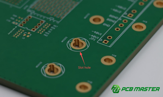
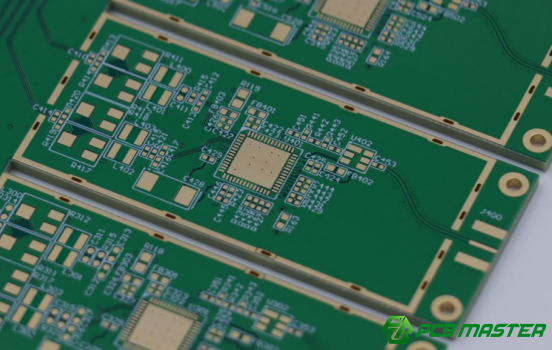
Slot holes, often referred to as elongated or irregular-shaped holes, are key features in PCB design, used for component placement, signal routing, or improving heat dissipation. Unlike traditional round holes, their unique shapes—such as rectangular, elliptical, or custom variations—bring about certain challenges in both design and manufacturing. These challenges, including dimensional accuracy, positioning, and surface finish, require careful planning and execution. In the following sections, we will explore the critical considerations for designing and processing slot holes, ensuring they meet the high standards required for optimal PCB performance.
How to Design the Right Slot Hole Size?
Designing the right slot hole size is crucial for ensuring the accuracy, functionality, and durability of your PCB. From selecting the correct width to managing the length-to-width ratio, every decision impacts the final quality of the board. In this section, we'll break down the essential factors you need to consider when designing slot holes, helping you avoid common issues like tool breakage, surface roughness, and material tearing during milling.
1. Size Requirements: How to Choose the Slot Hole Width and Aspect Ratio?
Minimum Slot Width and Drill Bit Selection:
The minimum width of a slot hole should typically be greater than or equal to 0.8mm. This ensures the drill bit doesn't break and prevents rough edges on the hole walls. Drill bits for slot holes are usually around 0.5mm in diameter, but this can vary depending on the board thickness and the manufacturer’s capabilities. A width that is too small can lead to increased stress on the tool, causing it to break or produce poor-quality edges. Therefore, choosing the correct slot width is essential to ensure a smooth and durable finish.
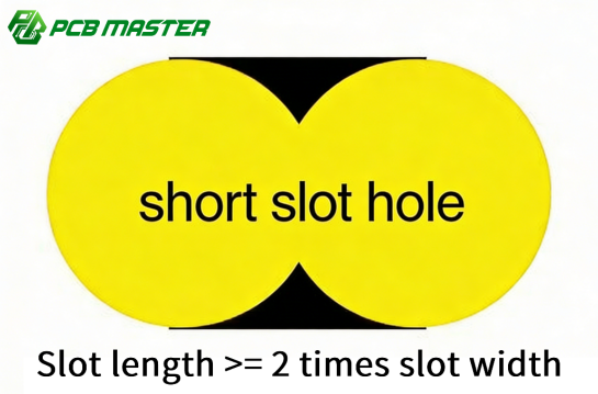
Aspect Ratio (Length-to-Width Ratio):
It is recommended that the length of the slot be at least twice its width (a length-to-width ratio of 2:1). A slot with a shorter length can be prone to deformation or misalignment during the machining process, leading to inaccuracies. Maintaining a 2:1 ratio ensures stability during fabrication and reduces the risk of errors or deformation. For example, a slot that is 4mm long and 2mm wide will be more stable and easier to machine than a 3mm long and 2mm wide slot.
2. How to Control the Distance Between Slot Holes and the Edge of the PCB?
Standard Distance Between Slot Edge and PCB Edge:
When designing slot holes, it is critical to ensure that the distance from the edge of the slot to the edge of the PCB is at least 1mm, but preferably 1.6 times the thickness of the board. This prevents the material from tearing or breaking during the milling process. If the slot hole is too close to the edge, the force from the milling tool can cause the edge of the board to chip or fracture, which compromises the quality and strength of the PCB.
How to Prevent Edge Tearing During Milling:
To avoid tearing, consider designing slots with sufficient space from the PCB edge. By maintaining a proper distance, the PCB remains stable during milling, and the forces exerted on the edges are distributed more evenly. Additionally, using a tool with the right cutting properties, such as a high-rigidity end mill, and controlling the cutting speed helps ensure the milling process goes smoothly without damaging the PCB’s edges. For instance, if you are machining a board that is 2mm thick, ensuring a 3.2mm distance between the edge of the slot and the edge of the PCB can help prevent tearing during fabrication.
What Key Points Should Be Considered in Slot Hole Shape and Position Design?
When designing slot holes for PCBs, the shape and position are just as important as the size. Small design choices can have a big impact on the performance and durability of the final product. In this section, we’ll explore key considerations for slot hole shapes and positioning, including how to avoid stress concentration, ensure even load distribution, and achieve a balanced layout. By following these principles, you can enhance the strength and reliability of your PCB design, preventing common issues during both manufacturing and operation.
1. Slot Hole Shape: How to Avoid Sharp Corners and Stress Concentration?
Designing Round-Edged Slot Holes:
Sharp corners at the ends of slot holes can lead to stress concentration, which may cause cracks or failure over time. To prevent this, it is recommended to design slot holes with rounded corners, specifically arcs that match the radius of the cutting tool. By avoiding sharp corners, you distribute stress more evenly along the slot, reducing the risk of structural weakness. For example, instead of a sharp corner at the end of a rectangular slot, design it with a rounded arc, which helps the material handle mechanical stresses more effectively and reduces the potential for fractures.
2. Slot Hole Position: How to Ensure a Rational Slot Layout?
Avoiding Overcrowded Slot Holes:
When placing multiple slot holes on a PCB, it’s essential to avoid crowding them together. Overly dense slot holes can lead to a variety of issues during manufacturing, including difficulties in milling, increased risk of mechanical failure, and compromised electrical performance. A well-spaced layout ensures that each slot hole can be precisely cut, and it provides enough material between them to maintain the integrity of the PCB.
For instance, when designing multiple slots, ensure there is enough distance between each to allow for clean cuts and minimize the risk of structural damage. This also helps in reducing the chances of interfering with adjacent components or signal pathways.
Ensuring Even Stress Distribution:
Improper slot positioning can lead to uneven stress distribution on the PCB. If slots are placed too closely together or in a non-symmetrical pattern, it can result in localized stress concentrations, which may cause the board to warp or fail under pressure. Distributing slot holes evenly across the PCB helps to balance the mechanical load, ensuring that no single area is over-stressed. A good design approach is to place the slots in a grid-like arrangement, keeping consistent spacing to balance the stress across the entire PCB.
3. Symmetrical Design: What Are the Requirements for Distributing Multiple Slot Holes?
Why Symmetrical Slot Hole Distribution Reduces Uneven Stress:
Symmetry in slot hole distribution is critical for minimizing stress imbalances during both the manufacturing and operational phases. When multiple slot holes are symmetrically placed, the forces acting on the PCB are more evenly distributed. This reduces the likelihood of warping or bending during the milling process and helps maintain the structural integrity of the PCB in use.
For example, in designs where multiple slots are required, a symmetrical arrangement (such as placing them along the central axis) ensures that the stresses are balanced from both sides. This not only enhances the mechanical stability but also ensures a more uniform performance throughout the PCB’s lifespa
Key Considerations in Material and Lamination for Slot Hole Design
When designing slot holes in PCBs, the choice of material and lamination process plays a crucial role in ensuring the strength, stability, and reliability of the final product. Key factors like the alignment of the slot with the fiber direction and managing the relationship between the inner copper layers and the slot holes can prevent common issues such as deformation and copper foil lifting.
1. Fiber Direction of the Base Material: How to Choose the Correct Slot Hole Direction?
Design Principle: Aligning the Long Side of the Slot with the Fiber Direction:
When designing slot holes, it is essential to align the long edge of the slot with the fiber direction of the base material, especially for fiberglass-reinforced PCBs. Fiber-reinforced materials, like FR4, have a grain-like structure, and the strength of the material is greater in the direction of the fibers. By aligning the slot with the fiber direction, you reduce the chance of deformations and improve the stability of the slot during manufacturing. This alignment ensures that the material will handle mechanical stresses more effectively without bending or cracking.
Why Does Fiber Direction Affect Slot Hole Deformation?
The orientation of the fibers in the base material significantly impacts how it behaves under stress. If the slot hole is cut against the fiber direction, the fibers are more likely to shift or break under pressure, causing the slot to deform. This can result in inaccurate hole dimensions or weak spots around the slot. By ensuring the slot runs parallel to the fiber direction, the forces are more evenly distributed, preventing deformation and ensuring the integrity of the PCB.
2. Multilayer Board Handling: How to Manage the Relationship Between Inner Copper Foil and Slot Holes?
How to Prevent Inner Copper Foil Lifting:
In multilayer PCBs, the inner copper foil layer can be vulnerable to lifting when slot holes pass through or near it. To prevent this, ensure that the slot hole design maintains an appropriate distance from the inner copper layers. If the slot hole is too close to the inner copper foil, the heat and mechanical stress during manufacturing could cause the copper to lift or delaminate. Proper design can prevent this issue by providing enough space between the copper layers and the edge of the slot hole.
Ensure Minimum Distance Between Inner Copper Foil and Slot Edge:
When designing slot holes that go through multiple layers, it’s crucial to maintain a minimum distance between the edge of the slot and the inner copper foil. This distance helps to avoid potential damage to the copper during the milling process and ensures the integrity of the signal path. Typically, the minimum distance should be at least 0.3mm from the copper foil to the edge of the slot hole. This ensures that the inner layers remain intact and that the slot hole does not cause electrical or mechanical issues in the PCB.
How to Ensure Slot Holes Do Not Misalign During Processing?
Ensuring slot holes remain perfectly aligned during processing is critical for maintaining the precision and integrity of your PCB design. Misalignment can lead to costly errors and affect the functionality of the final product. In this section, we’ll explore the key techniques—such as choosing the right processing methods, selecting high-quality tools, optimizing fixture setups, and controlling feed speeds—that will help you achieve accurate, well-aligned slot holes every time.
1. Processing Method: What’s the Difference Between CNC Milling and Drilling, and How to Ensure the Slot Hole Doesn’t Misalign?
CNC Milling vs. Drilling:
CNC milling is the preferred method for creating slot holes, especially for longer or irregularly shaped slots. Unlike drilling, which involves punching through the material, CNC milling uses rotating cutters to remove material in a controlled manner, ensuring precise dimensions and smoother edges. CNC milling provides better control over slot placement, minimizing the risk of misalignment. In contrast, drilling creates multiple overlapping round holes, which can lead to less precision, especially in slots with a smaller length-to-width ratio.
To avoid misalignment, CNC milling allows for one continuous cut that follows the design exactly, reducing the chances of the slot deviating during the process. The toolpath is programmed to follow the exact shape and position, ensuring that the slot hole remains accurate and consistent.
Why Add Auxiliary Holes When the Length-to-Width Ratio Is Less Than 2?
When the length-to-width ratio of the slot is less than 2, the slot may be more prone to deformation or misalignment during milling. In such cases, auxiliary holes are added at both ends of the slot to relieve stress and create a more stable cutting environment. These holes serve as "anchors," ensuring that the milling tool has a clear path and that the slot doesn't shift or become distorted.
2. Tool Selection and Control: How to Choose the Right Milling Cutter?
The Role of High-Rigidity Milling Cutters:
Choosing a high-rigidity milling cutter is essential for maintaining the accuracy of the slot hole. Harder materials like fiberglass-reinforced PCBs require cutters made from durable materials like carbide. High-rigidity cutters prevent tool deflection, which can lead to inconsistent cuts and misaligned slot holes. These cutters ensure smooth, precise milling and help maintain the integrity of the slot's dimensions throughout the process.
The Need for Controlling Feed Speed:
Controlling the feed speed during milling is equally important. If the speed is too high, it can cause excessive heat buildup and lead to tool wear, resulting in a rougher cut and potential misalignment of the slot hole. A slower feed speed allows for better control and smoother cuts, reducing the chances of deformation or misalignment. Adjusting the feed speed based on material thickness and cutter type ensures the slot hole is cut precisely without issues.
3. Positioning and Fixation: How to Ensure Precision in Slot Hole Processing?
The Importance of Precision Pin Holes:
For accurate slot hole positioning, it's critical to design precision pin holes at both ends or along the sides of the slot. These holes act as reference points during the milling process, ensuring that the slot is aligned properly. Using these reference holes helps to position the workpiece accurately on the milling machine, reducing the risk of misalignment or shifting during processing.
Vacuum Fixture to Reduce Material Movement:
Vacuum fixtures are an effective way to secure the PCB during milling, ensuring it stays in place and doesn't shift under the cutting forces. The vacuum system holds the material firmly, preventing any movement that could cause misalignment. This is especially useful when dealing with thin or flexible PCBs that are more likely to shift or bend. By ensuring the PCB remains stationary, vacuum fixtures help to achieve high-precision cuts and prevent any errors during the slot hole machining process.
4. Optimizing the Tool Entry Point: How to Avoid Material Tear-Out During Processing?
Choosing the Right Entry Point to Prevent Material Tear-Out:
The tool entry point, or "start point," is crucial to the quality of the slot hole. A poorly chosen entry point can lead to material tear-out, where the edges of the slot are damaged or rough. To avoid this, the entry point should be positioned at the center or on the outer edge of the slot, where it will not cause undue stress on the material. By carefully planning the entry point, you can prevent the tool from snagging the material and causing chips or tear-outs along the slot edges.
By optimizing the entry point and using the appropriate cutter, you can ensure the slot hole remains smooth and free from damage. This step, along with accurate positioning and controlled feed speed, ensures that the final slot hole meets the required dimensions and quality.
How to Optimize Slot Hole Drilling and Milling Data?
Optimizing slot hole drilling and milling data is essential for achieving precise, high-quality PCB manufacturing. Properly preparing your design files and making the right adjustments during the design phase can significantly reduce errors and improve the efficiency of the production process. In this section, we’ll explore the key steps, from marking slot holes for CNC routing in Gerber files to adding stress relief holes, ensuring your slots are perfectly aligned and structurally sound.
1. What Are the Slot Hole Design Requirements in Gerber Files?
Clearly Mark Slot Hole Design for CNC Routing:
In Gerber files, it's essential to explicitly mark the design for slot holes to be processed using CNC routing. This ensures that the fabrication team understands the specific requirements for these slots and chooses the correct toolpath for precise cutting. Without this clear indication, the system may default to other drilling methods, potentially leading to misalignment or suboptimal hole quality. By labeling slot holes as "CNC rout" or using similar terminology, you ensure that the slot is milled with the appropriate method, maintaining design accuracy.
For example, if you are designing a PCB with multiple slot holes, make sure to include these notations in the Gerber files and confirm that the routing tool is set up for the correct slot cutting operation.
2. When Should Stress Relief Holes Be Added, and How to Use Them?
When to Add Stress Relief Holes:
Stress relief holes are necessary when the length-to-width ratio of a slot hole is less than 2:1, as these slots are more prone to deformation during machining. A slot hole that is too short relative to its width may not handle the cutting forces well, leading to stress concentrations around the slot, which can cause distortion or misalignment. By adding stress relief holes, especially at both ends of the slot, you can help distribute the forces more evenly during the milling process, reducing the risk of material warping or shifting.
How to Add Stress Relief Holes:
Stress relief holes are typically small, circular holes that are added at the ends of the slot, either at the very tips or slightly offset from the slot’s boundaries. These holes create a "softened" area that reduces the cutting pressure on the slot's edges. For instance, if you’re designing a slot with a ratio of 1.5:1, you could add stress relief holes 1-2mm away from each slot end. This practice will help keep the material intact and minimize deformation, ensuring that the slot hole maintains its intended shape and size.
Electroplating Requirements in Slot Hole Design
When designing slot holes in PCBs, accounting for electroplating requirements is crucial to ensure the final product meets both mechanical and electrical specifications. Properly marking non-plated holes and compensating for the copper plating in plated slots will help prevent issues such as incorrect copper coating or misaligned slot dimensions.
1. How to Mark Non-Conductive Slot Holes (NPTH)?
How to Label NPTH to Avoid Incorrect Electroplating:
Non-conductive slot holes (NPTH) are those that should not undergo electroplating, as they do not require a copper coating. To avoid accidentally electroplating these holes, it's crucial to clearly mark them in your design files. In Gerber files, NPTH should be labeled specifically with the notation "NPTH" or "Non-Plated Through Hole." This label signals to the PCB manufacturer that these holes should not receive any copper coating during the plating process.
By marking these holes correctly, you ensure that the manufacturing process is followed as intended, preventing mistakes like unnecessary copper plating or damage to the non-conductive material. This is especially important when designing for multi-layer PCBs, where certain slots are not meant to conduct electricity but still require structural integrity.
Real-life Example:
For instance, if you design a PCB with slots that will be used for mechanical mounting or component placement, and these slots do not require electrical conductivity, you must label them as NPTH. This avoids copper plating, which could cause short circuits or reduce the effectiveness of the mounting process.
2. Electroplating Slot Holes: How to Account for Copper Plating Compensation?
How to Account for Slot Width Compensation After Electroplating:
Electroplating adds a layer of copper to the walls of plated through holes (PTH) or slots. This copper layer can cause the slot width to shrink slightly, as the plating thickens the hole walls. To compensate for this, it's essential to design the slot hole with a slightly wider width than required to account for the copper deposition. This compensation ensures that the final dimensions of the slot remain accurate after electroplating.
Why Slot Width Compensation is Important:
Without compensation, the electroplated copper could reduce the width of the slot too much, leading to issues with component fit or signal routing. For example, if your design calls for a 2mm wide slot, you might increase the width in the design by 0.1-0.2mm to ensure that after plating, the slot remains within the required dimensions. This ensures that after the copper is deposited, the slot will still function properly for component placement or signal routing.
Real-life Example:
In a scenario where a PCB is designed for high-frequency applications, and slot holes are used for specific routing or component placement, not accounting for copper plating compensation could cause signal integrity issues or physical misalignment. Compensating for the copper plating ensures the slot hole remains accurate, preventing such issues.
Conclusion
Achieving precision in slot hole design and manufacturing is crucial for ensuring the overall functionality and reliability of a PCB. By carefully considering each aspect—from the slot’s dimensions and shape to the choice of materials and processing methods—engineers can prevent potential issues that might compromise the integrity of the board. Proper design and accurate execution are key to producing PCBs that perform consistently and meet the highest standards of quality.
With this in mind, PCBMASTER, as a trusted and experienced PCB supplier, is committed to delivering high-quality, precision-engineered PCBs tailored to meet the specific needs of our customers. Through rigorous process controls and advanced manufacturing techniques, we ensure that every slot hole is fabricated with the utmost accuracy, supporting the long-term performance and durability of your PCB.
FAQs
1. How to Avoid Tool Breakage When Slot Width is Too Small?
Solution: Choose the Right Tool Size and Feed Speed:
When designing slot holes with very small widths, choosing the appropriate tool size is crucial to avoid tool breakage. If the slot width is too narrow, the tool can be under excessive stress, leading to a higher risk of breaking. To prevent this, it’s important to select a tool with a diameter suitable for the slot width, ensuring it can cut through the material without putting too much strain on the tool.
Additionally, controlling the feed speed is essential. A slower feed rate allows the tool to work more efficiently and reduces the chance of overheating or breaking. It also helps achieve a smoother finish without stressing the material. For example, if you are cutting a narrow slot, use a finer, high-quality carbide tool and reduce the feed rate to avoid sudden impacts or overloading the tool. By adjusting these parameters, you can ensure the machining process runs smoothly, even for smaller slots.
2. How to Prevent Inner Copper Foil Lifting in Multilayer PCBs?
Solution: Ensure Minimum Distance Between Slot Hole and Inner Copper Foil:
In multilayer PCBs, inner copper foils are vulnerable to lifting or delaminating, especially when cutting through the PCB layers. To avoid this issue, it’s essential to maintain a sufficient gap between the edge of the slot hole and the inner copper foil. Typically, this minimum distance should be at least 0.3mm. If the slot hole is placed too close to the copper layer, the cutting process could cause heat buildup or excessive pressure, leading to copper foil detachment.
Maintaining this gap also ensures that the integrity of the signal pathways in the PCB is preserved. For example, if your design includes a slot hole passing through a multilayer PCB, make sure that the slot is positioned with enough space from the inner copper to prevent damage to the foil, thereby improving the reliability and durability of the PCB.
3. How Does Symmetrical Design Help in Reducing Uneven Stress?
Solution: Symmetrical Slot Hole Distribution Reduces Stress Concentration:
When designing multiple slot holes, distributing them symmetrically across the PCB is an effective way to prevent uneven stress distribution. If slot holes are placed randomly or too close together, it can lead to localized stress concentrations. These concentrated stresses can weaken the PCB material and potentially cause it to warp, bend, or even fail under certain conditions.
By placing the slots symmetrically, stress is distributed more evenly across the board, reducing the risk of deformation. For example, placing multiple slots evenly on both sides of the PCB or along its centerline helps to balance the load, ensuring the material can withstand the stresses of both the manufacturing process and the end use. This approach not only improves the mechanical stability of the PCB but also helps maintain its electrical performance.
4. Why Should Sharp Corners Be Avoided in Slot Hole Design?
Solution: Avoid Stress Concentration by Using Rounded Corners:
Sharp corners in slot holes can lead to stress concentration, where forces are not evenly distributed, making the material more prone to cracking or failure. When designing slot holes, it is best to avoid sharp, angular edges and instead opt for rounded corners. The use of arcs or fillets at the ends of slots helps to reduce the stress concentration that would otherwise occur at sharp points.
For instance, instead of designing a slot with sharp 90-degree corners, a rounded shape can better withstand mechanical stresses, especially in high-stress areas. Rounded corners not only improve the mechanical reliability of the PCB but also help prevent issues like micro-cracking, ensuring that the board performs better and lasts longer.
5. Why is CNC Milling Recommended Over Drilling for Slot Holes?
Solution: CNC Milling Ensures Precise Slot Holes, Avoiding Misalignment and Deformation:
CNC milling is the preferred method for creating slot holes, especially for longer or irregularly shaped slots, as it provides far more precision compared to drilling. When drilling, the process involves multiple overlapping round holes, which can lead to misalignment and inaccuracies, especially when working with narrow or elongated slots.
On the other hand, CNC milling allows for the creation of a continuous, controlled cut, following the exact dimensions and shape of the design. This ensures that the slot is straight, aligned, and free of defects like burrs or uneven edges. For example, if you are working with a complex slot design, CNC milling ensures the final result is accurate and uniform, preventing any potential deformation or misalignment that might occur with drilling. This level of precision is crucial for ensuring the overall quality and functionality of the PCB.
Author Bio
Hi, I'm Carol, the Overseas Marketing Manager at PCBMASTER, where I focus on expanding international markets and researching PCB and PCBA solutions. Since 2020, I've been deeply involved in helping our company collaborate with global clients, addressing their technical and production needs in the PCB and PCBA sectors. Over these years, I've gained extensive experience and developed a deeper understanding of industry trends, challenges, and technological innovations.
Outside of work, I'm passionate about writing and enjoy sharing industry insights, market developments, and practical tips through my blog. I hope my posts can help you better understand the PCB and PCBA industries and maybe even offer some valuable takeaways. Of course, if you have any thoughts or questions, feel free to leave a comment below—I'd love to hear from you and discuss further!


