


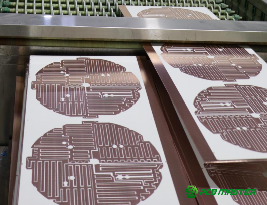
What Makes Extra-Long PCBs Different? Key Manufacturing Challenges and Process Controls
When a PCB gets significantly longer than standard production limits, it stops being just a bigger board. It becomes a manufacturing challenge of its own.
Once a board moves into the extra-long size range, issues that are usually manageable on standard PCBs—like dimensional stability, process consistency, handling stress, and equipment fit—can quickly become major yield risks. That’s why extra-long PCBs aren’t simply a scaled-up version of conventional boards. They require a different level of engineering review, process planning, and production control.
For design engineers, sourcing teams, and project managers, understanding what makes an extra-long PCB different is critical. It can help prevent a common problem in real-world projects: a board that passes prototype builds but becomes unstable or costly in volume production.
So what exactly makes an extra-long PCB special? The sections below break down the key manufacturing differences, process risks, and control points from a PCB production perspective.
What counts as an extra-long PCB?
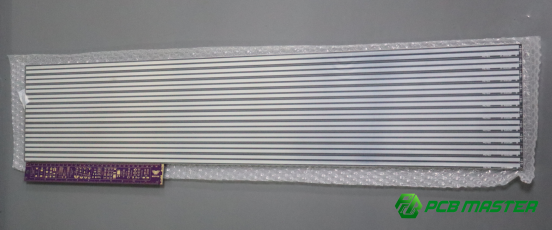
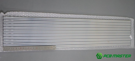
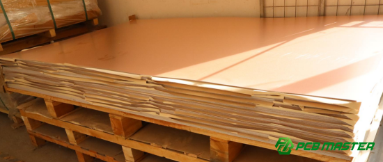
An extra-long PCB is a printed circuit board that exceeds the size limits of standard production equipment, requiring special handling, tooling, and process planning.
Extra-long PCBs are not just bigger boards—they introduce unique challenges in manufacturing. Typically, these boards exceed the standard length that a factory’s production line can process in one pass. Handling, exposure, drilling, plating, and testing all become more complex as the board grows in size.
What is the common industry definition of an extra-long PCB?
Industry standards generally consider boards longer than 600 mm (24 inches) as extra-long, but this can vary by factory.
l Typical Definition: Any PCB longer than the production line’s standard capacity.
l Threshold: Boards exceeding 600 mm (24 inches) are usually managed as extra-long PCBs.
l Factory Variations: Equipment size, transport system, and test platform limits may change the threshold. For example, a factory with a longer conveyor chain might treat 650 mm boards as standard, while another facility would classify them as extra-long.
Using a clear definition early in the design process helps engineers and procurement teams plan tooling, materials, and workflow to avoid surprises during production.
Why can’t extra-long PCBs be produced like regular PCBs?
Extra-long PCBs cannot follow standard production methods because their size amplifies mechanical and thermal challenges.
l Rigidity Issues: Longer boards are more prone to bending, sagging, or warping during transport and processing.
l Thermal Expansion: Heat from pressing, soldering, or plating causes the board to expand or contract, and errors accumulate over the extra length.
l Process Fit: Equipment like exposure machines, drill heads, or plating tanks may not accommodate the full board in a single pass.
l Systemic Challenge: These issues are interconnected. A sag in one area can affect drilling precision, which then affects plating and testing. Treating extra-long PCB production as a single-step process will likely lead to defects.
What are the key differences between extra-long and regular PCBs?
Extra-long PCBs differ from regular PCBs in equipment, process sensitivity, and production management.
l Equipment Compatibility: Standard machines may not handle the full length. Custom or segmented processes are often required.
l Narrower Process Window: Heat, pressure, and chemical processes must be tightly controlled to avoid warping or misalignment.
l Higher Process Stress Sensitivity: Mechanical stress, thermal cycling, and material expansion are amplified along the length.
l Specialized Fixtures: Custom tooling, carriers, or segmented panels are often necessary to stabilize the board.
l Yield and Scheduling Impact: Longer boards are more likely to fail or require rework, making production planning and delivery timelines more challenging.
What are the main manufacturing challenges of extra-long PCBs?
Extra-long PCBs create unique manufacturing challenges due to increased size, which amplifies mechanical stress, thermal effects, and alignment errors. These challenges impact every step from handling and drilling to exposure, plating, and testing.
Manufacturers must treat extra-long PCBs as a system-level problem, not just a longer version of standard boards. The main difficulty points include rigidity and mechanical deformation, thermal distortion, cumulative alignment errors, and higher equipment compatibility demands.
Why are extra-long PCBs more prone to rigidity issues and mechanical deformation?
The longer the PCB, the less rigid it becomes, making it more vulnerable to bending, sagging, and localized deformation.
l Self-weight Sagging: As the board length increases, its own weight causes the center to sag more noticeably. This can affect flatness during pressing, drilling, or soldering.
l Suspension during Transport: During automated transport, the board may be supported only at the ends, leaving the middle section unsupported. This leads to bending and potential stress points.
l Local Force Sensitivity: Operations like drilling holes, spray soldering, or flying probe testing apply localized pressure. On a long, unsupported board, these forces are more likely to create permanent deformations.
Why is thermal deformation harder to control on extra-long PCBs?
Longer PCBs react more unevenly to heat, and small thermal expansions accumulate into significant distortions.
l High-Temperature Processes: Pressing, soldermask curing, and hot-air solder leveling expose the board to heat that can expand or contract the material.
l Material CTE Amplification: Differences in coefficient of thermal expansion (CTE) between layers are magnified over longer distances, causing uneven shrinkage or warping.
l Cumulative Alignment Error: The longer the board, the more thermal shrinkage contributes to misalignment between layers, increasing the chance of defects in final assembly.
Why do extra-long PCBs accumulate alignment errors more easily?
Layer-to-layer registration becomes more challenging because small errors grow along the board’s length.
l Scaling Compensation Challenges: Exposure systems may struggle to uniformly scale patterns over long distances, leading to slight misalignments at board ends.
l Multi-Layer Stack Accumulation: In multi-layer PCBs, minor misalignment in inner layers can multiply across layers, resulting in significant cumulative errors.
l Dimensional Inconsistency: The board’s ends and middle may respond differently to heat and pressure, creating uneven expansion or contraction and causing alignment drift.
Why do extra-long PCBs require higher equipment compatibility?
Longer boards may exceed the processing capacity of standard machines, requiring special setups or segmented processes.
l Maximum Machine Size Limits: Exposure machines, etching lines, presses, plating lines, and test systems all have length constraints that can block single-pass processing.
l Transport and Support Limits: Conveyor tracks, chain supports, and carrier systems must accommodate longer boards without sagging or misalignment.
l Segmented Processing Needed: Some operations may require dividing the board into sections, increasing setup complexity and process time.
What special requirements exist for extra-long PCB pre-production evaluation?
Pre-production evaluation for extra-long PCBs focuses on verifying equipment capacity, process feasibility, and tooling support to ensure stable volume production. Early assessment prevents costly errors, delays, and rework.
Extra-long PCBs cannot be treated the same as standard boards. Early evaluation identifies constraints in equipment, handling, and process flow, ensuring the board can move through every manufacturing step without unexpected issues.
Why must maximum equipment processing size be confirmed first?
Confirming equipment limits early ensures the PCB can physically fit through all production steps and prevents surprises during full-scale production.
l Machine Limits: Exposure machines, presses, drilling systems, plating lines, surface treatment equipment, and testing machines each have a maximum board length and width they can handle.
l Process Planning: Knowing these limits allows engineers to decide whether segmented exposure, split drilling, special carriers, or external subcontracting is necessary.
l Impact on Volume Production: Equipment compatibility affects not just prototype feasibility but whether the board can be reliably produced at scale.
Why do extra-long PCBs require special scheduling and process flow evaluation?
Extra-long PCBs often cannot follow standard production schedules and require tailored routing, tooling, and interdepartmental coordination.
l Custom Scheduling: Standard line speeds may be too fast, so conveyor speeds may need to be reduced, or specialized carriers inserted to prevent sagging.
l Special Process Steps: Some steps may need manual intervention or segment-by-segment handling.
l Cross-Department Coordination: Engineering, CAM, manufacturing, quality, and equipment teams must collaborate to plan feasible process routes.
What key items should be confirmed during extra-long PCB pre-production evaluation?
Pre-production checks focus on board size, equipment compatibility, and process feasibility to avoid production bottlenecks.
l Maximum Board Size & Effective Machine Range: Verify the PCB fits each machine without modification.
l Carrier and Fixture Availability: Confirm if standard or custom carriers and supporting plates can hold the board.
l Segmented Exposure/Drilling Feasibility: Determine if the board can be processed in parts without affecting quality.
l Horizontal & Vertical Line Compatibility: Ensure board orientation and transport support are suitable for existing production lines.
l Testing Support: Check whether flying-probe testers or custom fixtures can reach all test points.
l Surface Finish Constraints: Ensure plating or soldermask processes can accommodate the board’s length.
What should be included in a recommended extra-long PCB DFM pre-review checklist?
A structured DFM checklist ensures all design and manufacturing risks are addressed before production.
l Board Length, Width, and Thickness Ratio: Identify potential sagging or handling issues.
l Layer Count & Symmetry: Verify balanced stack-up to reduce warping.
l Copper Thickness & Distribution: Check for uniformity to avoid stress points.
l Panelization Scheme: Decide whether the board requires segmented panels or bridging features.
l Alignment Holes & Process Edge Design: Ensure proper registration and handling.
l Critical Tolerances: Highlight dimensions that require stricter control.
l Surface Finish Type: Confirm process compatibility for soldermask, HASL, or ENIG.
l Final Testing Method: Ensure test coverage is achievable with available equipment.
What are the special material considerations for extra-long PCBs?
Extra-long PCBs require materials with high thermal stability and low expansion to reduce warping, alignment errors, and performance variations during manufacturing. Material choice is critical to ensure dimensional consistency, yield, and reliable final testing.
Because of their length, extra-long boards amplify even minor material inconsistencies. Selecting the right laminate and prepreg (PP) is essential to control warping, layer misalignment, and impedance drift.
Why are high Tg and low CTE materials recommended for extra-long PCBs?
High Tg and low CTE materials improve thermal stability and reduce deformation during heat-based processes.
l High Tg Benefits: Boards with high glass transition temperature (Tg) maintain their shape better during pressing, soldermask curing, and other heat-intensive processes.
l Low CTE Advantage: Materials with low coefficient of thermal expansion (CTE) limit expansion and contraction, reducing alignment drift and warping.
l Long Board Sensitivity: The longer the board, the more it relies on stable material properties, because small expansions or contractions are amplified over length.
What is the common logic for selecting materials for extra-long PCBs?
Material selection balances thermal stability, layer count, copper thickness, and dimensional consistency requirements.
l Standard FR-4 vs. High Tg FR-4: Standard FR-4 may be acceptable for short, low-layer boards. High Tg FR-4 is preferred for longer boards or high-temperature processes.
l High Layer Count or Copper Thickness: Boards with many layers or heavy copper are more prone to warping; high-stability laminates reduce this risk.
l Critical Impedance and Dimensional Consistency: Low CTE materials are essential when signal integrity and precise trace dimensions matter.
Why is using the same material batch and prepreg important for extra-long PCBs?
Consistency in material batches reduces process variability and cumulative shrinkage across the board.
l Batch Variability: Different material lots can have slightly different thermal expansion or shrinkage rates.
l Sensitivity of Long Boards: Even small differences are magnified over long distances, causing warping or misalignment.
l Process Compensation: Using the same batch narrows the range of adjustments needed in pressing, drilling, or plating, improving yield.
What typical problems occur if materials are chosen poorly?
Improper material selection can cause warping, alignment failure, impedance variation, and downstream assembly issues.
l Warping After Lamination: Boards may curve or twist, making them difficult to handle.
l Outer Layer Misalignment: Exposure and drilling errors increase when layers shift unpredictably.
l Impedance Deviations: Uneven copper expansion causes signal integrity problems.
l Board Bending During Soldering: Spray solder or hot-air leveling can further distort the board.
l Unstable Test Contacts: Warped boards may not sit correctly in test fixtures, causing false failures.
What are the special engineering and stack-up design points for extra-long PCBs?
Extra-long PCBs require careful engineering and stack-up design to control warping, stress, and alignment. This includes layer symmetry, copper balance, proper positioning of holes and edges, and avoidance of high-risk structures that amplify mechanical or thermal deformation.
Due to their length, small imbalances or design oversights can be magnified, making the engineering design phase critical to ensure flatness, dimensional accuracy, and signal integrity.
Why must extra-long PCBs emphasize absolutely symmetrical stack-ups?
Symmetrical layer arrangement prevents internal stress imbalances that cause warping after lamination.
l Core & Prepreg Arrangement: Asymmetrical stack-ups create differential internal stress during pressing.
l Warping Amplification: Longer boards show more pronounced bowing or twisting if layers are not balanced.
l Foundation for Flatness: Symmetry is the baseline requirement for controlling bending, sagging, and board twist.
Why is copper balance more critical in extra-long PCBs?
Uneven copper distribution creates localized heat absorption and mechanical stress, which can cause warping and affect signal quality.
l Stress from Uneven Copper: Heavy copper areas expand differently under heat, causing bending or twisting.
l Length Amplification: Over a long board, small differences in copper area are magnified into significant warping.
l Impact on Manufacturing: Copper balance affects etching uniformity and impedance consistency, critical for high-speed signals.
What should be considered for process edges, alignment holes, and auxiliary structures?
Extra-long boards need wider edges, carefully placed holes, and optional support structures to maintain stability during processing.
l Process Edge Width: Wider edges enhance stability during transport and prevent board sagging.
l Alignment Holes: Layout must consider cumulative error over the board’s length, ensuring proper layer registration.
l Auxiliary Structures: Adding bridges, stiffeners, or local support areas can prevent bending and improve handling through presses, drills, and plating lines.
What high-risk design structures should be avoided in extra-long PCBs?
Certain structural choices can weaken rigidity or amplify process challenges on long boards.
l Excessive Long Slots: Too many longitudinal cutouts reduce board stiffness and increase warp risk.
l Large Single-Sided Copper Areas: Heavy copper on one side creates stress imbalance, worsening flatness issues.
l Critical Edge Traces: Placing sensitive traces near the board edge raises the risk of scratches during handling.
l Fine Lines on Long Boards: Ultra-thin trace and spacing combined with long dimensions narrow the process window and increase defect likelihood.
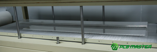
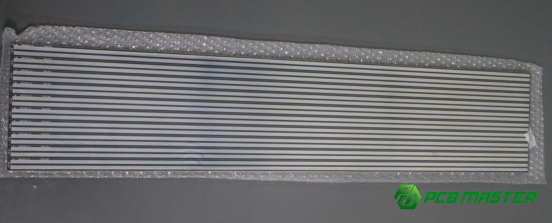
Why do extra-long PCBs often require special panelization and carrier design?
Extra-long PCBs frequently need customized panelization and carriers because their size reduces rigidity, increases handling risks, and challenges standard production equipment. Proper design ensures stability, reduces defects, and improves testability.
Without panelization or reinforced carriers, long boards can sag, misalign, or be damaged during transport, drilling, plating, and surface finishing.
When should extra-long PCBs be panelized instead of run as single boards?
Panelization is recommended when a single board is too flexible, risky to transport, or exceeds equipment capacity.
l Low Rigidity: Single boards may bend or sag during line transport, risking scratches or drill misalignment.
l Equipment Limits: When board length surpasses the maximum size a machine can handle, segmenting into panels is necessary.
l Improved Production Stability: Panelization enhances board support and simplifies testing with flying-probe or fixture methods.
What are the common panelization methods for extra-long PCBs?
Extra-long PCB panelization methods improve rigidity, support, and later separation while balancing stress.
l Mouse-Hole (Stamp) + Bridges: Reinforces rigidity during transport and supports post-processing.
l V-Cut + Bridges: Facilitates board separation but requires careful stress control to prevent edge cracks.
l Strengthened Process Edges: Extra-wide or reinforced edges stabilize boards during movement and reduce sagging.
Practical tip: Combining a V-cut with strategic bridges and reinforced edges can ensure both mechanical support and smooth separation for high-yield production.
What are the core principles of extra-long PCB panel design?
Panel design must balance rigidity, process stress, and testability.
l Primary Focus on Rigidity and Transport: Ensure boards remain flat and stable throughout the line.
l Manage Separation Stress: Bridges and V-cuts should minimize deformation during final depanelization.
l Protect Critical Areas: Avoid placing bridges near key components to prevent interference or stress concentration.
l Consider Test Fixture Compatibility: Panel layout should align with flying-probe or fixture testing paths to maintain accuracy.
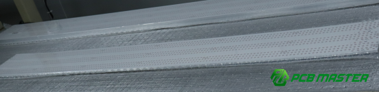
Why must extra-long PCBs pay attention to tool and carrier design?
Carriers and tooling stabilize the board across multiple processes, reducing sag, jamming, scratches, and soldering deformation.
l Line Stability: Carriers hold the board flat during transport, lamination, drilling, and plating.
l Defect Prevention: Proper carriers prevent bending, stuck boards, scratches, and warping during hot processes.
l Critical for Volume Production: A well-designed carrier often determines whether an extra-long board can be produced reliably at scale.
What features should dedicated extra-long PCB carriers have?
Specialized carriers should provide strength, thermal resistance, precision, and multi-process compatibility.
l High Strength and Heat Resistance: Prevent deformation under press, soldermask curing, or hot-air solder leveling.
l Precision Alignment: Accurate positioning ensures layer registration and drilling accuracy.
l Even Support Points: Proper distribution prevents sagging in long boards.
l Multi-Process Compatibility: Carriers must work across exposure, drilling, plating, and testing.
l Reusable and Easy to Maintain: Durable design reduces cost and downtime.
What are the special process requirements for inner-layer patterning of extra-long PCBs?
Inner-layer fabrication for extra-long PCBs requires careful exposure, alignment, and etching controls. Due to board length, standard single-pass processes may not work, making segmenting, alignment, and defect inspection critical for quality and signal integrity.
Extra-long boards amplify errors in exposure, registration, and copper etching, so precision in every step is essential to maintain dimensional accuracy and impedance consistency.
Why might extra-long PCBs require segmented exposure?
Segmented exposure is needed when the board exceeds the working area of standard exposure machines.
l Full Board Too Large: Exposure equipment cannot cover the entire PCB in a single pass.
l Limitations of Traditional Machines: Standard photolithography systems are designed for smaller boards, making full-board exposure impossible.
l Alignment Challenges: Segmenting introduces the need for precise stitching to prevent pattern misalignment between sections.
What are the critical control points during segmented exposure?
Accuracy depends on alignment marks, overlap control, and scaling compensation.
l Alignment Targets: Targets must be designed for segmented stitching to maintain consistent registration between sections.
l Overlap and Stitching Accuracy: Overlapping areas must have controlled tolerance to prevent gaps or over-etching.
l Longitudinal Scaling Compensation: Adjustments should consider material shrinkage, temperature, and humidity to correct expansion or contraction along the board.
Why is LDI preferable for extra-long PCBs?
LDI (Laser Direct Imaging) offers flexible alignment and local deformation correction, reducing cumulative registration errors.
l Flexible Registration: Laser imaging can adjust for minor warpage or material shrinkage along the board length.
l Local Correction: Allows fine-tuning of pattern placement in problematic sections.
l Reduced Accumulated Error: Minimizes the risk of layer-to-layer misalignment that is more pronounced on long boards.
What issues should be closely checked after inner-layer etching?
Post-etch inspection ensures uniform copper thickness, trace width, and impedance consistency.
l Copper Thickness Uniformity: Both board ends and center must have consistent copper to avoid impedance variations.
l Line Width Variation: Check if trace width changes along the length, which can cause signal inconsistencies.
l Critical Impedance Areas: Inspect key high-speed signal regions for uneven etching.
l Local Over-Etch or Under-Etch: Identify areas where copper may be missing or over-removed, which can cause shorts or open circuits.
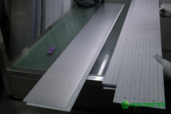
What are the special considerations for drilling and via metallization of extra-long PCBs?
Drilling and via metallization in extra-long PCBs require precise process control due to increased risk of misalignment, uneven plating, and mechanical stress. Ensuring accuracy during these stages is vital for maintaining signal integrity, board flatness, and high yields.
Extra-long boards amplify issues such as alignment errors, inconsistent plating, and mechanical deformation. Therefore, careful drilling, copper plating, and hole filling are crucial for maintaining quality and avoiding defects.
Why is drilling more prone to hole misalignment in extra-long PCBs?
Drilling long boards introduces dimensional instability and uneven support, making hole alignment more difficult.
l Poor Longitudinal Stability: Once the material is fixed, the board's length makes it more prone to slight shifts, reducing drilling accuracy.
l Increased Stress and Vibration: The central portion of the board experiences more stress and vibration during the drilling process, which can affect hole position.
l Support Differences: The edges and center of the board are supported differently, leading to uneven pressure and an increased risk of hole misalignment.
What are the key process controls during drilling of extra-long PCBs?
To ensure accurate drilling and minimize defects, multi-head drilling, optimized support, and vibration control are critical.
l Multi-Head or Segmented Drilling: Using multiple drill heads or segmenting the drilling process reduces the chance of misalignment.
l Increased Backing Board Hardness: A harder backing board increases support at the edges, preventing warping or movement during drilling.
l Optimized Clamping and Holding: Proper clamping mechanisms reduce board shifting or vibration, ensuring more accurate hole placement.
l Reduce Vibration During Drilling: Control vibration to prevent tool deflection, which can lead to oversized holes or misaligned vias.
Why is horizontal copper plating preferred for extra-long PCBs?
Horizontal plating is better suited for long boards as it provides more uniform support and reduces distortion.
l Vertical Plating Risks: Vertical hanging can cause the board to warp or bend under its own weight, affecting plating consistency.
l Even Horizontal Support: Horizontal plating offers more uniform support across the board, reducing the risk of deformation.
l More Consistent Copper Distribution: Horizontal plating results in more even copper deposition, preventing thick or thin areas on the via walls.
How to avoid uneven plating during via metallization on extra-long PCBs?
Uniform plating requires managing current density, adjusting the plating process, and using advanced monitoring techniques.
l Balanced Current Density: Ensure consistent current density across the board, especially between the two ends and the middle.
l Programmable Rectifiers: Use programmable rectifiers to divide the board into zones, adjusting current for each section to achieve uniform copper thickness.
l Real-Time Thickness Monitoring: Continuously monitor the plating process to ensure that copper thickness remains consistent across the board.
l Enhance Solution Flow: Improve solution circulation to prevent stagnant areas where uneven plating may occur.
What are the special considerations for outer-layer patterning and etching of extra-long PCBs?
Outer-layer patterning and etching for extra-long PCBs require careful management of alignment, temperature fluctuations, and etching consistency. The increased length of the board makes it more sensitive to misalignment, inconsistent chemical exposure, and other process variables. Precise control at every stage is crucial to ensure quality and avoid defects.
Why is cumulative alignment error more likely in outer-layer exposure of extra-long PCBs?
The longer the PCB, the more it is affected by thermal expansion, temperature gradients, and inconsistent material behavior, leading to alignment errors during exposure.
l Thermal Expansion: The longer the board, the greater the impact of thermal expansion and contraction. This effect can cause misalignment during the exposure process.
l Temperature and Humidity Variations: Different parts of the PCB are exposed to varying temperature and humidity levels, leading to uneven material shrinkage.
l Inadequate Scaling Compensation: Traditional scaling methods may not sufficiently cover the board’s length, leading to cumulative misalignment across the board.
How to properly compensate for dimensions during outer-layer exposure on extra-long PCBs?
Dimension compensation involves adjusting for thermal effects, material shrinkage, and alignment accuracy through targeted adjustments and advanced imaging techniques.
l Longitudinal Compensation Model: Develop a compensation model based on material batch characteristics to account for longitudinal shrinkage.
l Temperature and Humidity Adjustments: Use real-time data to adjust scaling coefficients, minimizing distortions due to environmental factors.
l Key Area Alignment: Implement independent alignment strategies for critical areas to ensure accurate positioning of components.
l Real-Time Compensation with LDI: Laser Direct Imaging (LDI) allows real-time adjustments to compensate for deformations as the exposure process proceeds.
Why is it harder to control etching uniformity on extra-long PCBs?
Etching uniformity is more challenging on extra-long PCBs because of uneven chemical distribution and varying exposure to etching agents.
l Uneven Chemical Exposure: Different parts of the PCB have varying rates of chemical exchange due to differences in exposure time and material composition.
l Spray Pressure and Angle Sensitivity: Spray pressure, angle, and conveyor speed have a more significant impact on long boards, causing inconsistent etching.
l Position-Based Etching Factor: The etching factor (rate of material removal) can vary across the board, especially at different lengths, making it more difficult to achieve uniform etching.
What are the key optimization measures for etching on extra-long PCBs?
To optimize etching, adjustments must be made to the spray pressure, conveyor speed, and chemical flow, ensuring uniform exposure across the entire PCB.
l Optimize Spray Pressure and Angle: Adjust the spray pressure and angle to ensure uniform coverage across the board, especially for longer lengths.
l Fine-Tune Conveyor Speed: Optimize the conveyor speed to ensure consistent exposure to the etching chemicals for both ends and the middle of the PCB.
l Enhance Chemical Exchange at Both Ends: Increase the flow of etching chemicals to the edges of the PCB to improve consistency in material removal.
l Increase Line Width Sampling Points: Perform more frequent line width measurements at key positions (beginning, center, and end) to monitor etching consistency.
What are the special considerations for soldermask and surface finishing processes in extra-long PCBs?
Soldermask and surface finishing processes in extra-long PCBs are more challenging due to increased size and gravity effects. These boards require careful handling during printing, curing, and plating to avoid defects like ink sagging, uneven thickness, and warping. Precision in every step is crucial for ensuring reliable performance and maintaining consistent quality.
Why is soldermask more prone to ink sagging or uneven thickness on extra-long PCBs?
The large size and limited support during the process make soldermask more vulnerable to gravity-induced sagging and uneven application.
l Increased Gravity Impact: The larger the PCB, the more noticeable the effect of gravity. Without sufficient support, the soldermask ink tends to sag, causing uneven thickness.
l Difficulty in Maintaining Flatness: Longer boards are harder to keep flat during single-pass printing, making it difficult to control uniformity.
l Ink Flow Variations: Long boards experience differences in ink flow, which can lead to regions where the soldermask is too thin or too thick.
What soldermask processes are recommended for extra-long PCBs?
Using multiple printing steps and liquid photoimageable (LPI) inks helps improve soldermask accuracy and reduce defects.
l Two-Step Printing Process: Print one side, pre-cure, and then print the other side to ensure a more even application and better adhesion.
l LPI Ink for Better Accuracy: Liquid Photoimageable (LPI) Ink offers better precision than traditional inks, especially for fine-pitch components.
l Increased Support During Processing: Adding extra support helps minimize deformation during the printing and curing process, ensuring a smoother surface.
Example: A 650 mm PCB was printed in two stages with pre-curing, significantly improving the evenness of the soldermask, especially at the edges and center.
Why is HASL riskier for extra-long PCBs?
The size and temperature effects make hot air solder leveling (HASL) more challenging for extra-long PCBs, leading to increased risk of warping and sagging.
l Temperature-Induced Warping: The high temperature used in HASL can cause the board to warp, especially for long boards, which have more mass and surface area.
l Solder Bath Chain Adjustments: The angle and stability of the solder bath conveyor system can become more critical for long boards, affecting the final result.
l Thermal Stress and Flatness Issues: The cumulative heat exposure increases the likelihood of thermal stress, which may lead to warping or uneven flatness.
How to control deformation during the HASL process for extra-long PCBs?
Using proper fixtures, adjusting the conveyor system, and optimizing the heating and cooling process can reduce deformation risks during HASL.
l Use Fixtures or Specialized Supports: Using custom racks or fixtures to support the board during the soldering process can minimize bending and sagging.
l Adjust Chain Angle and Board Orientation: Fine-tuning the angle of the conveyor and the board's position ensures that the PCB stays flat during the process.
l Optimize Pre-Heat and Soldering Temperature Curves: Control the temperature ramp-up and cooling processes to reduce thermal stress and ensure uniform solder coating.
l Improve Cooling after Soldering: After the soldering process, manage cooling carefully to prevent sudden temperature changes that could lead to board warping.
What considerations should be made for gold plating (ENIG) on extra-long PCBs?
Gold plating for extra-long PCBs requires better liquid flow control, filtration, and active monitoring to ensure uniformity in metal deposition.
l Even Liquid Flow: Ensure consistent liquid flow in the plating tank to maintain uniform plating along the length of the PCB.
l Improved Chemical Circulation and Filtration: Strengthen the circulation and filtration system to prevent stagnation and uneven plating in certain areas.
l Monitor Active Differences: Watch for differences in plating activity between the ends and the middle of the PCB, especially since the board’s length may result in varying plating conditions.
l Prevent Nickel-Gold Thickness Variations: Consistently monitor and adjust plating conditions to avoid fluctuations in the thickness of the nickel and gold layers along the board.
What are the special requirements for testing and final inspection of extra-long PCBs?
Extra-long PCBs require careful testing and inspection due to their size, shape, and unique production challenges. Testing processes need to be adapted for better accuracy, while final inspection should address concerns like warping, dimensional stability, and surface defects.
Why do flying probe tests for extra-long PCBs usually require segmentation?
Flying probe testing often requires segmentation for extra-long PCBs because of the limitations of the probe machine’s effective testing range, board deformation, and the need for more accurate positioning.
l Limited Testing Range: Flying probe machines have a limited range, meaning that boards longer than their testing capacity must be tested in segments.
l Deformation and Coordinate Drift: As extra-long boards flex or warp during handling, the probe’s coordinates can shift, making it difficult to ensure accurate testing across the entire board.
l Improved Precision with Segmentation: Dividing the board into smaller segments for testing helps maintain alignment and repeatability, improving the overall accuracy of the test results.
What are the key control points for flying probe testing on extra-long PCBs?
To ensure successful testing, several critical factors need to be controlled, including coordinate calibration, deformation compensation, and contact stability.
l Coordinate Calibration for Segments: Each segment of the PCB needs to be calibrated separately to ensure that the flying probe's coordinate system matches the physical layout of the PCB.
l Deformation Compensation: Parameters must be set to account for deformation that can occur in long PCBs during testing. This ensures that the probe compensates for slight shifts or bends in the board.
l Platform Flatness Verification: The flatness of the test platform must be verified to ensure stable contact and accurate probing.
l Contact Stability at Both Ends and Center: Verify that the flying probe maintains stable contact at both the edges and the middle of the PCB, which is especially challenging for long boards due to their size.
When is it necessary to customize a test fixture for extra-long PCBs?
Custom test fixtures are necessary when flying probe testing is inefficient due to large batch sizes, high testing point density, or when there are strict requirements for testing consistency and speed.
l Large Batch Sizes and Inefficient Flying Probe Testing: When dealing with a large volume of extra-long PCBs, the time required for flying probe testing can become inefficient. Custom fixtures can significantly speed up the process.
l High Testing Point Density or Complex Structures: If the PCB has a high density of testing points or complex geometries, flying probes may struggle to provide accurate and fast results. A custom fixture designed to handle these features will increase efficiency.
l Higher Demands for Testing Speed and Consistency: When testing speed and consistency are critical, a custom fixture can improve both, ensuring that each board is tested thoroughly and accurately in a more streamlined manner.
What quality indicators should be prioritized during the final inspection of extra-long PCBs?
During the final inspection of extra-long PCBs, it’s important to focus on warping, dimensional stability, hole quality, surface finish, and physical defects.
l Warping and Bowing: The longer the PCB, the more likely it is to warp or bow during manufacturing. Inspecting for flatness is critical to ensuring that the board remains usable for its intended applications.
l Dimensional Stability: Confirm that the board’s shape and size are consistent and that there are no discrepancies between the specified dimensions and the actual product.
l Hole Quality: Check that the copper plating inside the holes is consistent across the length of the board, especially between the ends and the center, where differences may occur due to uneven heat distribution.
l Surface Finish Consistency: Ensure that the surface finish is even throughout, with no areas of excessive or insufficient coating.
l Physical Defects: Inspect for scratches, abrasions, and other physical damage that could compromise the PCB's performance or aesthetics.
What are the most common production risks for extra-long PCBs and how can they be resolved?
Extra-long PCBs face unique production challenges, including warping, alignment issues, uneven copper plating, and transport-related defects. These risks can be mitigated with proper process control, adjustments to equipment settings, and the use of specialized materials and techniques.
Why is warping after lamination the most common issue with extra-long PCBs?
Warping occurs due to several factors, such as asymmetric layer stacking, unbalanced copper distribution, misaligned heating and cooling processes, and uneven stress release during cooling.
l Asymmetric Layer Stacking: If the layers of the PCB are not symmetrically stacked, it can create internal stress during lamination, causing the board to warp.
l Copper Distribution Imbalance: Uneven copper plating across the board leads to differing thermal expansion rates, which contributes to warping.
l Mismatched Heat Pressing Curves: If the temperature profile used during lamination isn’t suited for long boards, the heat application can cause uneven stress distribution.
l Uneven Stress Release During Cooling: Cooling too quickly or unevenly after lamination can result in warping as different parts of the board cool at different rates.
Solutions for Warping
l Optimize Heating and Cooling Curves: Adjust the temperature rise and fall rates during lamination to ensure even distribution of heat.
l Ensure Symmetrical Lamination Structure: Ensure the PCB’s core and prepregs (PP) are symmetrically arranged to minimize internal stress.
l Use Heavy Pressing Immediately After Lamination: Apply additional weight or pressure immediately after lamination to flatten the board during cooling.
l Choose Stable Materials: Use high-stability laminate materials (e.g., high Tg, low CTE) to reduce the chance of thermal expansion-related issues.
Why do alignment errors accumulate on extra-long PCBs?
Alignment issues arise from the thermal expansion and contraction of long PCBs, as well as errors introduced during segmented exposure or processing.
l Thermal Expansion and Contraction: As the board expands and contracts due to heat, it can distort the alignment of components and layers, especially over longer lengths.
l Errors in Segmented Exposure/Processing: If the PCB is processed in segments, slight misalignments between segments can accumulate, leading to alignment errors.
l Traditional Compensation Models Don't Fit: Standard compensation models that work for smaller PCBs may not account for the unique characteristics of long boards.
Solutions for Alignment Issues
l Use LDI for Real-Time Compensation: Laser Direct Imaging (LDI) offers more flexibility and accuracy for real-time compensation of alignment errors.
l Develop Batch-Specific Scaling Compensation Models: Create compensation models that are customized for each batch, considering the specific material properties and dimensions of each batch.
l Optimize Alignment Target Layout: Redesign alignment targets to better suit long boards, ensuring that segments align accurately.
l Increase Measurement Feedback at Critical Points: Add additional measurement points during the manufacturing process to monitor alignment in real-time.
Why do extra-long PCBs often have uneven copper plating thickness?
Uneven copper plating is usually caused by irregular current distribution, inconsistent chemical flow, and the significant electrical field differences between the edges and center of the PCB.
l Uneven Current Distribution: The electrical current used in the plating process doesn’t always spread evenly across a large board, causing some areas to receive more copper than others.
l Inconsistent Chemical Flow: The chemicals used in the electroplating process may not flow uniformly over long boards, leading to plating imbalances.
l Electrical Field Variations: Longer boards create more variation in the electrical field, especially between the center and edges, leading to inconsistent copper deposition.
Solutions for Copper Plating Issues
l Use Programmable Rectifiers: Implement programmable rectifiers to better control the flow of current during plating, ensuring uniform copper deposition across the board.
l Adjust Current Density in Zones: Use a zonal approach to adjust the current density in different sections of the board to maintain even plating.
l Improve Circulation and Spray Flow: Enhance the circulation and spray systems to ensure that the chemicals reach every part of the board uniformly.
l Increase Monitoring Points: Place additional monitoring points to check the copper thickness at different locations on the board, allowing for better quality control.
Why do extra-long PCBs face issues with board handling, scratching, and transport anomalies?
These issues are caused by insufficient rigidity, inadequate support along the transport tracks, high conveyor speeds, and a lack of soft protection during transport.
l Insufficient Rigidity: Longer boards are less rigid and more prone to bending or flexing, which can lead to transport damage.
l Inadequate Support Along Transport Tracks: If the PCB is not properly supported throughout its journey along the conveyor, it can easily become misaligned or damaged.
l Excessive Conveyor Speed: High-speed conveyors can cause extra-long PCBs to flex or get caught, increasing the risk of scratches or transportation errors.
l Lack of Soft Protection: Without soft padding or cushioning, long PCBs are vulnerable to scratching or physical damage during handling.
Solutions for Handling Issues
l Clean and Calibrate Transport Tracks: Regularly clean and calibrate the transport tracks to ensure smooth and accurate board movement.
l Add Soft Guide Wheels or Auxiliary Supports: Install soft guide wheels or additional support systems to prevent the board from bending or shifting.
l Reduce Conveyor Speed: Slow down the conveyor speed to ensure that the board stays securely in place without excessive movement.
l Optimize Edge and Fixture Design: Adjust the edge and fixture design of the board carrier to provide more support, preventing scratching and misalignment.
How should the key process control points for extra-long PCBs be systematically managed?
Managing extra-long PCB production requires an integrated approach, focusing on process control, cross-department collaboration, and consistent monitoring. Special care must be taken to address stress accumulation and ensure that each stage of production works in synergy to maintain quality.
Why must extra-long PCBs adopt a "full-process stress control" approach?
The issue of stress accumulation in extra-long PCBs is not confined to one specific process but spans across multiple stages. Small deformations in earlier steps can be magnified later, leading to larger defects. Ensuring consistent stress management throughout the entire process helps maintain the overall quality of the PCB.
l Stress Is Cumulative Across Processes: A deformation in one stage (e.g., lamination or drilling) can be carried over to subsequent stages, like exposure, etching, or copper plating. This makes it essential to manage stress not just at one point, but throughout the whole production chain.
l Small Early-Stage Deformations Can Be Magnified Later: Minor distortions at the start of production may seem insignificant but can worsen as the board progresses through each stage, resulting in defects in later steps like exposure alignment or plating.
l Yield Control Requires "Process Chain Coordination": Ensuring good yield requires all processes to work together harmoniously. Focusing on individual process fixes won’t solve the overall problem, as each part of the process affects the next.
What key process parameters should be controlled during mass production of extra-long PCBs?
Managing parameters like temperature stability, material consistency, press curve settings, and plating conditions is essential for maintaining the quality of extra-long PCBs during production.
l Temperature and Humidity Stability: Consistent environmental conditions prevent material expansion or contraction, ensuring that the PCB doesn’t warp or misalign during production.
l Material Batch Consistency: Using materials from the same batch ensures uniformity in thermal properties, expansion rates, and other material characteristics, which is crucial for large boards.
l Lamination Press Curve: The heat application during lamination must be optimized to prevent stress during cooling. Incorrect press curves can lead to warping or alignment issues.
l Exposure Compensation Parameters: Adjust exposure settings to account for long PCB dimensions, as thermal expansion or contraction can affect accuracy.
l Drilling Support Conditions: Proper support during drilling minimizes the risk of misalignment and ensures hole accuracy.
l Plating Current Distribution: Uneven current distribution during copper plating can cause thickness variations, leading to weak points in the PCB.
l Conveyor Speed and Support Methods: Long PCBs require slower conveyor speeds and adequate support to avoid bending and misalignment.
What are the most effective process monitoring methods for extra-long PCBs?
To ensure high-quality production, key monitoring steps include measuring the full size of first pieces, checking thickness at multiple points, applying SPC controls, tracking deformation trends, and creating compensation databases for batch-specific adjustments.
l Full-Size First Piece Measurement: Ensure that the first PCB produced meets all size and quality standards before continuing production. This sets a reference for the rest of the batch.
l Multi-Point Thickness Inspection at Both Ends and Center: Perform thickness measurements at critical locations to monitor uniformity and detect any early signs of deformation.
l SPC Control of Critical Processes: Statistical Process Control (SPC) ensures that each process step, such as lamination, drilling, and plating, stays within acceptable tolerances.
l Tracking Deformation Trends: Monitor and track any changes in PCB shape or size over time to prevent larger issues down the line.
l Batch-Specific Compensation Databases: Create compensation strategies for each production batch based on the unique characteristics of materials and equipment to prevent alignment and sizing errors.
What management model should be used when introducing extra-long PCB projects?
A collaborative, multi-department approach is crucial when introducing extra-long PCB projects. The process should include cross-functional reviews, validation of the first samples, small-batch testing, and a risk management system.
l Cross-Department Reviews (Engineering, CAM, Manufacturing, Quality): Ensure that all departments are aligned from the start. Engineering designs, CAM settings, manufacturing processes, and quality controls should be reviewed together.
l First Piece Validation + Small-Batch Trials + Parameter Confirmation: Once the first piece is validated, conduct small-batch trials to fine-tune parameters. Only after these trials should full-scale production begin.
l List Critical Risk Points: Identify potential risks early and create a mitigation plan. For example, consider material-related risks or equipment limitations that may affect long PCB production.
l Pre-Validate Equipment Capability: Ensure that equipment can handle the unique requirements of extra-long PCBs, especially the maximum board size and weight.
Which Process Solutions Can Improve Yield for Extra-Long PCBs?
Extra-long PCBs face unique challenges, but selecting the right materials and processes can significantly enhance yield. This includes using high-stability materials, implementing advanced imaging techniques, custom carriers, specialized plating, and developing dedicated process windows.
Solution 1: Use a High-Stability Material System
Choosing materials with high thermal stability and low thermal expansion ensures better performance in the production of extra-long PCBs, enhancing overall yield.
l High Tg FR-4: High glass transition temperature (Tg) FR-4 materials provide better heat resistance, reducing the risk of deformation during high-temperature processes like soldering and lamination. This helps in maintaining structural integrity throughout the manufacturing cycle.
l Low CTE Materials: Low coefficient of thermal expansion (CTE) materials help minimize the risks associated with thermal expansion and contraction, which can cause warping or misalignment, particularly in long PCBs.
l Same Batch PP and Core Material: Using materials from the same batch for both the prepreg (PP) and core ensures consistency in thermal expansion rates, which is crucial for the stability of extra-long boards.
Solution 2: Adopt LDI and Deformation Compensation Strategies
Laser Direct Imaging (LDI) and deformation compensation strategies significantly improve the alignment precision and reduce cumulative errors in extra-long PCBs.
l Improves Alignment Precision: LDI technology provides high accuracy in pattern transfer, which is essential for long PCBs where even minor misalignments can be amplified.
l Reduces Longitudinal Cumulative Errors: By using real-time compensation techniques, LDI helps in minimizing the cumulative dimensional errors that can accumulate along the length of extra-long boards.
l Ideal for High-Precision Circuitry: This solution is particularly suited for products with fine lines and small features that require extremely high precision in their patterning.
Solution 3: Configure Dedicated Carriers and Tooling
Using custom carriers and tooling ensures better handling and stability of extra-long PCBs during production, minimizing deformation risks in key processes like soldering, coating, and testing.
l Enhances Line Transport Stability: Specialized carriers or fixtures help evenly distribute the weight of extra-long boards, preventing bending and ensuring smooth transport through production lines.
l Reduces Risk of Soldering, Coating, and Testing Deformation: Custom carriers help secure the PCB during critical processes like soldering (HASL), surface coating (solder mask), and electrical testing, reducing deformation.
l Critical for Mass Production Consistency: Dedicated tooling is key to ensuring consistent quality across large production runs, ensuring that every PCB meets the same high standards.
Solution 4: Use Plating by Section and Multi-Point Thickness Monitoring
Plating by section and constant thickness monitoring improve copper distribution consistency, which is essential for the reliability and performance of extra-long PCBs.
l Improves Copper Thickness Consistency Across Length: By using a segmented plating approach, it’s easier to control the copper deposition in different areas of the board, ensuring uniformity.
l Enhances Hole Copper Reliability: The process ensures uniform copper thickness on vias, which is crucial for the structural integrity and electrical performance of the PCB.
l Reduces Soldering and Reliability Risks: Uniform copper thickness prevents issues like cold solder joints and ensures that the PCB can withstand high-stress environments without failure.
Solution 5: Establish a "Dedicated Process Window" Through Pilot Production
Establishing a specific process window for extra-long PCBs through pilot production helps optimize process parameters and ensures stable production for large batches.
l Cannot Simply Copy Standard PCB Parameters: Extra-long PCBs require specific process parameters that are different from those for standard-size boards due to their increased dimensions and thermal sensitivity.
l Build Custom Compensation and Process Parameters: Through small-batch pilot production, manufacturers can identify and adjust the specific process variables (e.g., temperature curves, exposure settings) needed to handle the unique demands of extra-long boards.
l Small-Batch Validation Locks in Best Process Combination: Running small batches allows fine-tuning of process variables and helps ensure that the most efficient and reliable production parameters are locked in before moving to mass production.
Key Considerations for Engineers When Dealing with Extra-Long PCB Production
Extra-long PCBs present unique challenges. Designers, procurement teams, and project managers must focus on critical factors to ensure successful production, from structural integrity to procurement and project management.
Top 3 Design Considerations
Designers should focus on structural symmetry, copper balance, and panelization to ensure the PCB performs well throughout the production process.
l Structural Symmetry: The layout of the PCB layers should be symmetrical to avoid internal stress and warping during production. Any asymmetry can cause the board to bow or twist, especially in extra-long sizes. Symmetry is crucial for maintaining dimensional stability.
l Copper Balance: Uneven copper distribution across the board can cause localized heating during processes like soldering, leading to warping or misalignment. Ensuring balanced copper distribution helps minimize these risks, making the production process more predictable.
l Panelization and Manufacturability of the Process Edge: Panelizing the PCB into smaller, manageable pieces is essential for handling extra-long PCBs. The edges should be designed with ease of manufacturing in mind, ensuring they can be securely held during processing without causing deformation.
Top 3 Procurement Considerations
Procurement engineers should focus on the factory’s capacity, specialized tooling, and past experience with similar products to ensure successful long-term production.
l Factory's Maximum Processing Size and True Production Capability: Before choosing a supplier, verify that the factory can consistently handle extra-long boards. Ensure the equipment they use is capable of processing the specific dimensions and that they have reliable production history.
l Experience with Dedicated Carriers/Lines for Extra-Long PCBs: Specialized carriers and dedicated production lines are essential for handling extra-long boards efficiently. Confirm if the factory has experience using these tools, as this can significantly affect production quality.
l Proven Track Record in Plating, Solder Mask, and Testing: Ensure the supplier has a proven track record with the specific challenges of extra-long PCBs, particularly in processes like plating, solder masking, and electrical testing.
Top 3 Project Management Considerations
Project managers must focus on ensuring sufficient time for trial production, accepting special tolerances, and cross-department collaboration to ensure smooth development and manufacturing.
l Reserve Time for Trial Production: For extra-long PCBs, trial runs are crucial. They allow for testing of production processes and adjustments to be made to ensure that production targets are met efficiently and effectively.
l Accept Special Tolerances and Risk Assessments: Due to the size and complexity of extra-long boards, be ready to accept special tolerances. A thorough risk assessment will help address potential challenges and allow for better planning.
l Cross-Department DFM Confirmation During NPI: During the New Product Introduction (NPI) phase, ensure that all departments involved in the production process (e.g., engineering, manufacturing, quality assurance) review and confirm the Design for Manufacturability (DFM). This prevents surprises during the production phase and minimizes delays.
Practical Judgment Standard: Prototype ≠ Stable Mass Production
Just because a prototype works doesn’t mean large-scale production will succeed. Successful mass production requires careful consideration of equipment, processes, tooling, and quality control.
l Prototypes May Rely on Manual Intervention: During the prototype phase, manual intervention can help fix issues that might not appear in smaller runs. However, manual fixes aren’t scalable for mass production.
l Mass Production Requires Coordination Across Equipment, Processes, Tooling, and Quality: For long PCBs to be produced efficiently at scale, all processes must be coordinated, from equipment calibration to process management and tooling.
l True Capability Is Measured by Yield, Delivery Time, and Consistency: It’s essential to focus on key metrics such as yield rates, delivery time, and consistency across all boards. These factors provide a clearer picture of whether a factory can handle mass production successfully.
PCBMASTER’s Expertise in Extra-Long PCB Manufacturing
PCBMASTER is a leading provider of extra-long PCBs, specializing in boards up to 1.8 meters in length for rigid materials like FR-4 and aluminum, and up to 2.5 meters for flexible polyimide materials. Our expertise in extra-long PCB manufacturing is built on precision and reliability, making us the preferred partner for industries like LED displays, industrial control, and automotive electronics.
Key Capabilities:
l Advanced Equipment: PCBMASTER uses cutting-edge machinery tailored to handle extra-long PCBs. Our high-precision CNC machines, large-area imaging systems, and vacuum lamination presses ensure each board meets strict accuracy and quality standards.
l Material Flexibility: We offer a broad range of materials, including rigid options like FR-4 and aluminum (up to 1.8m), and flexible polyimide (up to 2.5m) for applications requiring flexibility. This flexibility allows us to meet the specific demands of high-performance applications like power distribution, signal routing, and thermal management.
l Thickness Range: Our extra-long PCBs can be manufactured with a thickness range from 0.4mm to 5.0mm, allowing for customization based on the specific performance and durability needs of each project.
l Precision and Quality Control: PCBMASTER’s in-house quality control team ensures that all extra-long PCBs are produced to the highest standards, maintaining dimensional accuracy and ensuring the boards meet performance requirements for various applications.
l Fast Turnaround: We pride ourselves on offering quick turnaround times, with samples produced in 3-5 days and mass production completed in 10-15 days, allowing us to meet tight deadlines without compromising on quality.
l Customization: We provide full customization options for dimensions, material choices, thicknesses, and circuit layouts. Our team works closely with clients to design and produce extra-long PCBs that meet their exact specifications.
Conclusion
Extra-long PCBs are crucial for industries that require large-scale, high-performance circuit boards. Their unique design and manufacturing challenges demand specialized materials, advanced techniques, and precise production processes. From ensuring rigid materials like FR-4 and aluminum can meet the needs of power-sensitive applications, to offering flexible polyimide options for large-scale, adaptable designs, the right approach to extra-long PCB production can make all the difference in achieving reliability, performance, and efficiency.
With advancements in technology, industry standards, and the expertise of companies like PCBMASTER, businesses can confidently pursue their most demanding projects. By focusing on key considerations such as material stability, precision alignment, and customization, you can ensure that your extra-long PCBs will provide the durability and functionality your project requires.
Whether you're developing LED displays, industrial automation systems, or high-power electronics, extra-long PCBs are the foundation for success in large-scale, high-performance applications.
FAQs
Do ultra-long PCBs always require high Tg materials?
Not necessarily, but high Tg, low CTE materials are usually better suited for extra-long boards. If the process involves multiple high-temperature steps, a high layer count, or strict dimensional tolerances, it’s recommended to prioritize these materials for improved stability and performance.
Can ultra-long PCBs be produced directly on regular PCB production lines?
In rare cases, it’s possible, but you’ll need to confirm the maximum size capability of each process, the support structure for the carrier, and the testing method. Just passing a single process doesn't guarantee smooth production across the entire workflow. Full-scale, stable mass production often requires specialized equipment and processes.
Which process is most likely to encounter issues when manufacturing extra-long PCBs?
There isn’t a single process that stands out as problematic, but the most common issues tend to arise during lamination, outer layer alignment, electroplating, soldering, and testing. These challenges often stem from the cumulative impact of multiple processes working together.
After successful prototyping, can mass production of extra-long PCBs still face issues?
Yes, and it’s quite common. Prototypes often rely on manual adjustments, but mass production demands stable equipment, fixtures, and well-defined process windows to ensure consistent quality and performance over time.
Is it essential to use custom carriers for extra-long PCBs?
If the length significantly exceeds the comfortable production limits of standard lines, or if the product has low rigidity or undergoes multiple high-temperature processes, custom carriers are highly recommended. They can drastically improve yield, appearance, and consistency during production.
Author Bio
Hi, I'm Carol, the Overseas Marketing Manager at PCBMASTER, where I focus on expanding international markets and researching PCB and PCBA solutions. Since 2020, I've been deeply involved in helping our company collaborate with global clients, addressing their technical and production needs in the PCB and PCBA sectors. Over these years, I've gained extensive experience and developed a deeper understanding of industry trends, challenges, and technological innovations.
Outside of work, I'm passionate about writing and enjoy sharing industry insights, market developments, and practical tips through my blog. I hope my posts can help you better understand the PCB and PCBA industries and maybe even offer some valuable takeaways. Of course, if you have any thoughts or questions, feel free to leave a comment below—I'd love to hear from you and discuss further!

