


Designing Thick-Copper PCBs: Considerations and Optimization Tips
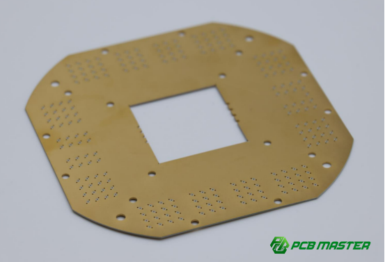
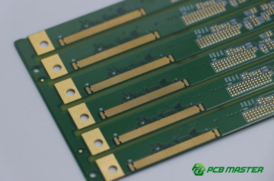
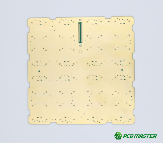
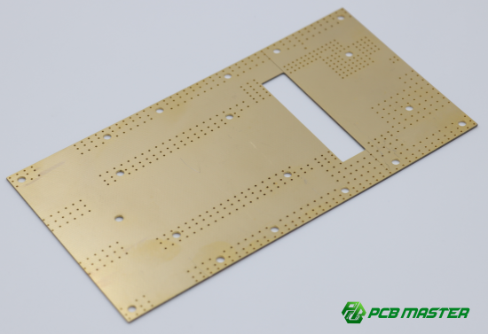
Thick-copper PCBs refer to printed circuit boards with significantly higher copper thickness than standard designs, typically ≥2 oz on outer layers and ≥3 oz on inner layers. These boards are widely used in high-current and high-power applications such as power supplies, automotive electronics, industrial control systems, and renewable energy equipment. The thicker copper allows the board to carry more current and dissipate heat more effectively, but it also makes manufacturing more complex. For example, compared to a standard 1 oz PCB, a thick-copper board may experience stronger etching effects and uneven plating, which directly impacts reliability.
This article focuses on the key design considerations and optimization tips for thick-copper PCBs. The goal is to help designers understand the main challenges—such as thermal concentration, stress imbalance, and fabrication accuracy—and how to address them early in the design stage. By applying practical guidelines, such as increasing trace width, optimizing copper distribution, and selecting proper materials, engineers can improve manufacturability, reduce defects, and ensure long-term reliability. In real projects, early collaboration with PCB manufacturers often prevents costly redesigns and significantly improves production yield.
Why Is Thick-Copper PCB Design Challenging?
Thick-copper PCB design is challenging due to issues with uneven heat distribution, thermal stress, and the high precision required in the manufacturing process to avoid defects like side-etching.
1. Thermal Concentration and Stress Imbalance
Thick-copper PCBs are often used in high-power and high-current applications, where heat is generated as current flows through the copper traces. The thicker the copper, the better the PCB can handle this heat, but it also means that the heat is more concentrated in certain areas. This can lead to uneven heat distribution, which increases the risk of thermal stress. When heat builds up in specific spots, it can cause the PCB to warp or even crack. For instance, if a high-current trace is located near a small component, the temperature difference between them can create mechanical stress, leading to failure. To prevent this, thick-copper PCB designs need to incorporate proper heat dissipation features like heat sinks, spreaders, or thermal vias.
Additionally, copper has a different rate of thermal expansion compared to other materials on the PCB, like the resin or fiberglass substrate. This mismatch can result in mechanical stress when the board heats up and cools down during operation. If not managed properly, this stress can lead to cracks, delamination, or other forms of failure. Therefore, controlling thermal expansion and minimizing stress through design features like proper via placement or using materials with similar expansion rates is essential for ensuring durability.
2. High Precision Required in Pattern Creation
Creating the intricate patterns and traces needed for thick-copper PCBs requires high-precision manufacturing techniques. One of the biggest challenges in this process is the side-etching effect, which occurs when the copper etching process is not perfectly controlled. The thicker the copper, the more challenging it becomes to achieve precise, clean traces. During the etching process, if the settings are not correct, copper can be "etched" unevenly, causing unwanted thinning along the edges of traces or pads. This not only affects the integrity of the PCB but also increases the risk of short circuits or circuit failures.
Manufacturers must also adhere to strict process capabilities, as thick-copper PCBs require more advanced equipment and materials than standard boards. For example, the etching process for thick copper needs to be carefully managed to ensure that the etching solution reacts uniformly across the board. A small mistake in process control can lead to poor-quality boards, resulting in significant production delays or increased costs. Ensuring that the design follows DFM (Design for Manufacturing) guidelines and is in line with the capabilities of the PCB manufacturer is crucial to avoid these issues. This requires careful planning and communication with the manufacturing team to ensure the design can be produced reliably and with high quality.
Key Considerations When Designing Thick-Copper PCBs
When designing thick-copper PCBs, key aspects to focus on include trace width and spacing, hole and annular ring design, surface finish selection, material choice, and effective thermal management to ensure reliability and manufacturability.
1. Trace Design
Minimum Trace Width/Spacing Requirements
To avoid issues like incomplete etching and short circuits, it’s important to design wider traces and larger spaces than usual. For thick-copper PCBs, side-etching during the copper removal process can result in thin spots in the trace, leading to poor electrical performance or failures. To minimize these risks, the trace width should be at least 1.5 to 2 times larger than what is typically required for regular copper PCBs. This extra width helps ensure the trace remains intact after etching and reduces the likelihood of short circuits. For example, in a high-current application, using a wider trace will help prevent overheating and ensure the board performs reliably over time.
Copper Surface Uniformity
Ensuring uniform copper distribution across the PCB is critical. If there are large isolated copper pads or areas with very thin traces surrounded by thick copper, it can lead to uneven plating during manufacturing. This could result in over-plated areas (excessive copper buildup) or under-plated areas (risk of broken connections or weak points). One strategy to ensure uniform copper distribution is to use a grid pattern or thermal pad designs that balance the current flow, especially when designing large copper areas.
2. Hole and Annular Ring Design
Minimum Annular Ring Requirements
The annular ring is the copper area around the hole that connects the inner and outer layers. For thick-copper PCBs, the minimum annular ring must be larger than standard designs due to the increased material thickness. For outer layers, an annular ring of at least 8 mils is recommended, while for inner layers, it should be at least 10 mils. This ensures proper copper plating around the hole and prevents the copper from separating under thermal or mechanical stress. Smaller annular rings can result in weak connections, especially when subjected to high heat or vibration.
Increasing Annular Ring for High-Current Vias
For high-current vias, it’s essential to further increase the annular ring to enhance the strength of the connection. Larger vias are required to carry the additional current, and a larger annular ring ensures that there is enough copper to maintain structural integrity during thermal cycling and mechanical stress. A good example of this would be in power electronics, where vias are used to carry large currents, and a failure in via design could lead to overheating or even board failure.
3. Solder Mask and Surface Finish
Solder Mask Bridge Challenges and Solutions
On thick-copper PCBs, solder mask bridges—thin connections of solder mask that link adjacent pads—are often difficult to maintain. During the soldering process, these bridges can crack or tear, causing electrical shorts. To prevent this, it’s crucial to ensure that there is sufficient space between pads and that the solder mask is applied in multiple layers to create a strong and continuous barrier. In some designs, a thicker solder mask layer can be used to prevent solder mask bridge issues, especially in high-density areas.
Surface Finish Selection: HASL, Gold Plating, and OSP
When selecting the surface finish for thick-copper PCBs, the choice depends on the application requirements. HASL (Hot Air Solder Leveling) is the most common and affordable option, but it may not provide the smoothness needed for high-density designs. Gold plating or immersion gold provides a smoother surface and better durability, but it requires a thicker nickel layer to avoid nickel migration. For high-current applications, OSP (Organic Solderability Preservative) is often not ideal due to its lower thermal performance. Choosing the right surface finish is key to ensuring long-term reliability, especially when dealing with large currents.
4. Lamination and Material Selection
Impact of Dielectric Layer Thickness on Lamination Quality
The dielectric layer, or the insulating material between copper layers, plays a crucial role in the lamination process of thick-copper PCBs. If the dielectric is too thin, it may not fully support the thick copper traces, leading to poor adhesion or weak insulation. A general rule of thumb is that the dielectric thickness should be at least as thick as the inner copper layer. For example, if using 3 oz copper for the inner layers, the dielectric layer should be thicker than the copper to prevent issues like delamination or voids. This ensures that the PCB has the mechanical strength and insulation needed to handle high voltages and currents.
Why High Tg Materials are Better for Thick-Copper PCBs
High Tg (Glass Transition Temperature) materials are better suited for thick-copper PCBs because they offer higher thermal stability. These materials can handle the thermal expansion caused by the high currents running through the thick copper without degrading or warping. Materials with a Tg of 170°C or higher are preferred because they maintain their integrity under heat stress, ensuring that the PCB performs reliably in demanding applications, such as automotive or industrial control systems. Using low-Tg materials may lead to thermal cycling problems, causing delamination or failure over time.
5. Thermal Management Design
Heat Sink and Via Design for Thermal Optimization
Thick-copper PCBs often require specialized thermal management to ensure heat is dissipated effectively. One common method is to use heat sink vias, which are small holes in the PCB that connect to the heat-generating components and help conduct heat away. These vias should be placed near high-power components, like power transistors or voltage regulators, and should be designed to carry thermal energy to the backplane or heat sink. For example, in power electronics, a well-placed via network can prevent excessive heat buildup, reducing the risk of thermal damage.
Utilizing Large Copper Areas as Heat Dissipators
In thick-copper PCB designs, large copper areas can be used as effective heat dissipation tools. By designing large copper pads that are connected to the ground or power planes, the PCB can spread heat over a larger surface area, improving heat transfer and reducing thermal hotspots. This is particularly beneficial in applications where heat generation is a constant concern, such as in high-power LED lighting or electric vehicles. Large copper areas not only help with heat dissipation but also contribute to the mechanical stability of the PCB, ensuring that the board remains flat and resistant to warping.
Thick-Copper PCB Design Optimization Tips
Thick-copper PCB design optimization tips include early collaboration with manufacturers, proper corner and copper thickness handling, and avoiding V-CUTs to ensure manufacturability, minimize warping, and improve thermal and electrical performance.
1. Early Communication and Collaboration with PCB Manufacturers
Why is early communication with the PCB factory important?
Before starting the design of a thick-copper PCB, it is crucial to communicate key design parameters and objectives with the PCB manufacturer. This early discussion ensures that the design aligns with the manufacturer’s capabilities, avoiding potential issues during production. Key details like copper thickness, trace width, hole size, and surface finish should be clarified from the beginning. For example, a PCB manufacturer with limited capability may struggle to produce a design with very fine traces or require adjustments to fit their processes.
How does DFM (Design for Manufacturing) impact the design process?
DFM (Design for Manufacturing) is a set of guidelines that optimize the design for easier, cost-effective manufacturing. By collaborating with the PCB factory early on, designers can align the design with DFM rules, which ensures that the board can be produced with minimal defects, fewer design changes, and within budget. For instance, simplifying the layout to reduce the number of vias or using standard materials that the factory is comfortable with will make the manufacturing process smoother and more cost-efficient.
2. Design Handling for Corners and Special Areas
What is the importance of corner treatment and step copper thickness design?
Corners in thick-copper PCBs should be rounded or beveled to reduce mechanical stress. Sharp corners act as stress concentrators, which can lead to cracks or failures, especially when the PCB is exposed to thermal expansion. By using rounded corners or chamfering, the design becomes more resilient to thermal and mechanical stresses. In addition, using a step copper thickness design (where copper thickness gradually increases or decreases in certain areas) can improve the PCB's overall thermal performance, as it helps manage heat distribution more effectively.
What are the advantages and limitations of localized copper thickening?
Localized copper thickening is an effective method for improving the performance of specific areas on the PCB that need to carry more current. For example, certain components like power transistors or high-current traces may benefit from thicker copper to handle the increased load. However, while this technique can enhance electrical and thermal performance, it also has limitations. It can increase manufacturing complexity and cost, as the board requires additional processing steps. Moreover, not all PCB manufacturers offer this capability, so it’s essential to confirm whether your factory can handle localized copper thickening before proceeding with the design.
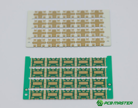
3. Panelization and Warping Control Design
Why should V-CUT be avoided in thick-copper PCB design?
V-CUT is often used to separate PCBs during production, but it is not ideal for thick-copper boards. The V-CUT process can create stress points that lead to trace damage, especially on thicker copper layers. Additionally, the deep cuts required for V-CUT can compromise the integrity of the PCB, leading to potential warping or fractures. As a solution, "stamp hole + bridge" methods are recommended for separating PCBs. This method involves creating small holes and connecting the boards with a bridge, ensuring that the boards stay intact during separation while maintaining structural integrity.
How can copper distribution be controlled to prevent warping?
Thick-copper PCBs are prone to warping due to uneven copper distribution, which causes the board to expand and contract at different rates. To prevent this, it’s important to maintain symmetrical copper distribution across the PCB. If one area of the board has much more copper than another, the board may warp when it is heated or cooled. A common technique to mitigate this risk is to balance the copper by adding or removing copper from different areas. For example, if there is a large copper area on one side of the PCB, adding a similar copper area on the opposite side can help maintain balance and prevent warping.
Thick-Copper PCB Design Success Checklist
The Thick-Copper PCB Design Success Checklist includes confirming core design elements like trace width, spacing, and dielectric thickness, selecting the right solder mask and surface finish, and finalizing material choices, panelization methods, and corner treatments for optimal manufacturability and reliability.
1. Confirming Core Design Elements: Trace Width, Spacing, Annular Ring, and Dielectric Layer Thickness
Why is confirming core design elements essential for thick-copper PCBs?
When designing thick-copper PCBs, it is crucial to confirm core parameters like trace width, spacing, annular ring size, and dielectric layer thickness before proceeding with manufacturing. Thick copper can cause side-etching during the etching process, so it is essential to design wider traces and larger spacing to prevent defects like short circuits and incomplete etching. For example, traces should be at least 1.5 to 2 times wider than in standard designs to account for potential side-etching.
The annular ring (the copper around drilled holes) must be larger for thick-copper boards. A minimum of 8 mils for outer layers and 10 mils for inner layers ensures proper copper plating around the holes, which is essential for electrical integrity.
Dielectric layer thickness also needs to be confirmed as it directly affects the insulation and mechanical strength of the PCB. For thicker copper layers, the dielectric layer should be at least as thick as the copper to avoid issues like delamination or electrical breakdown. These measures ensure that the PCB can handle high current without issues during both manufacturing and operation.
2. Key Considerations for Solder Mask and Surface Finish
What should you keep in mind when selecting the solder mask and surface finish?
Selecting the right solder mask and surface finish is vital for the functionality and longevity of thick-copper PCBs. When dealing with thick copper, solder mask bridges—thin connections between adjacent pads—can easily break, leading to short circuits. To avoid this, ensure adequate spacing between pads and apply the solder mask in multiple layers. This will help in preventing solder mask tears and ensure a more reliable PCB.
For surface finishes, it’s important to choose the one that fits your application. HASL (Hot Air Solder Leveling) is commonly used, but it might not be the best option for thick-copper PCBs, especially when smoothness is needed. Gold plating or immersion gold are excellent choices for ensuring durability and providing a smooth surface for high-density designs. However, OSP (Organic Solderability Preservative) should generally be avoided for thick-copper boards due to its lower thermal performance.
A proper surface finish ensures that the PCB will have good solderability, which is critical for high-reliability applications.
3. Final Confirmation of Material Selection, Panelization, and Corner Treatment
Why is it important to confirm material selection, panelization method, and corner treatment?
Material selection directly impacts the performance and reliability of thick-copper PCBs. High Tg materials (above 170°C) are recommended because they provide better resistance to thermal stress, ensuring that the board won’t warp or fail under high temperatures. Using low-Tg materials can result in delamination or warping due to mismatched thermal expansion between the copper and substrate.
For panelization, avoid using V-CUT as it introduces mechanical stress that can damage traces and lead to warping in thick-copper boards. Instead, use the stamp hole and bridge method to separate PCBs without compromising their integrity.
Corner treatment is another important consideration. Sharp corners in thick-copper PCBs can act as stress concentrators, leading to potential cracks or failures when the board is exposed to thermal or mechanical stress. To mitigate this, corners should be rounded or beveled, distributing the stress evenly across the board and improving its overall durability.
By confirming material choices, panelization methods, and corner treatments, designers ensure that the PCB will perform reliably over its lifespan and will not fail due to manufacturing defects.
Conclusion
Designing a thick-copper PCB involves several key considerations that ensure the board is manufacturable and reliable. The design must account for wider trace widths, larger spacing, and careful selection of materials to handle the increased thermal and electrical demands. Effective solder mask application and surface finish choices are also crucial to prevent defects like solder mask bridges and ensure good solderability. By collaborating closely with manufacturers and confirming the design details early, designers can avoid costly mistakes and improve the production process.
Optimizing the design process helps improve both production efficiency and product reliability. By addressing these factors upfront, manufacturers can reduce rework, minimize production defects, and ensure that the final product performs reliably in high-power applications. Additionally, following a structured design checklist and adhering to best practices ensures that thick-copper PCBs meet both electrical and mechanical performance standards.
For those looking for high-quality PCBs and PCBA services, PCBMASTER stands out as an experienced supplier dedicated to delivering top-notch products. With years of expertise, PCBMASTER provides reliable, precision-engineered solutions for thick-copper PCBs, ensuring that every product meets the highest industry standards. Whether you are looking to prototype or mass-produce high-performance boards, PCBMASTER is committed to supporting your project with quality and efficiency.
FAQs
1. Why Do Thick-Copper PCBs Require Larger Trace Widths and Spacings?
Thick-copper PCBs require larger trace widths and spacings primarily due to the side-etching effect during the etching process. When thick copper layers are etched, the etching solution tends to eat away not just the copper on the surface but also undercut the edges, creating a narrowing effect called side-etching. This can lead to insufficient trace width, especially for high-current applications, and could cause short circuits or open circuits if the traces are too thin. To avoid such issues, the trace width should be designed to be 1.5 to 2 times wider than what would be used for standard copper thickness to account for this side-etching, ensuring that the traces remain robust and free from defects during manufacturing.
2. How to Choose the Right Surface Finish for Thick-Copper PCBs?
Choosing the right surface finish for thick-copper PCBs depends on the specific requirements of the application and the conditions under which the PCB will operate. HASL (Hot Air Solder Leveling) is commonly used, but it is not ideal for applications requiring precise smoothness or high current handling, as it can create an uneven surface. For high-density designs, immersion gold or gold plating is a better choice, offering a smooth, durable surface with excellent solderability. OSP (Organic Solderability Preservative) is generally not recommended for thick-copper boards due to its lower thermal performance. The choice of surface finish should also consider factors like thermal stress, current load, and environmental conditions, ensuring optimal soldering and electrical performance.
3. What is Step Copper Thickness Design, and How Does it Improve Cost-Effectiveness?
Step copper thickness design refers to a method where the copper thickness is adjusted in different regions of the PCB, typically thicker copper in high-current areas and thinner copper in low-current regions. This design improves cost-efficiency by reducing the amount of copper used where it’s not necessary, while still providing sufficient thickness where needed for high-current handling. The benefit is that this approach can help reduce material costs and manufacturing complexity, as less copper is required in non-critical areas. Additionally, this method maintains the necessary electrical and thermal performance without increasing the overall cost of the board.
4. How to Avoid Thermal Expansion Issues in Thick-Copper PCBs?
Thermal expansion is a significant issue for thick-copper PCBs, as copper expands at a different rate than the substrate material, causing warping or delamination under temperature changes. Effective thermal management is key to preventing this. One solution is to ensure uniform copper distribution across the PCB, which helps to balance the thermal expansion across different areas. Additionally, heat sinks or thermal vias can be added to help dissipate heat more evenly. The dielectric material used should also have a high Tg (glass transition temperature) to withstand thermal stresses without degrading. By optimizing copper layout and using appropriate thermal management techniques, thermal expansion problems can be significantly reduced.
5. When to Choose a Metal Core PCB as an Alternative to Thick-Copper Boards?
A metal core PCB (MCPCB) is a good alternative to thick-copper PCBs when there is a need for enhanced heat dissipation in applications with high thermal loads, such as LED lighting, power electronics, or high-performance computing. MCPCBs typically use materials like aluminum or copper as the base layer, which offers superior heat conduction compared to standard PCBs. If the application requires significant heat dissipation and reduced thermal resistance, MCPCBs are preferred because they provide excellent thermal management and ensure the components stay cool, thereby improving the longevity and reliability of the board. For low to moderate heat applications, thick-copper boards are typically sufficient, but for high-heat scenarios, MCPCBs are the better choice.

