


Mastering Multilayer PCB Design: Key Techniques and Best Practices
Multilayer PCB design is very important in modern electronics, enabling devices to become smaller, faster, and more powerful. As technology advances, the need for highly efficient, reliable, and compact circuit boards has never been greater. Whether you're designing a smartphone, a medical device, or an industrial control system, mastering multilayer PCB design is essential to ensuring your product performs at its best.
However, creating a multilayer PCB involves much more than just stacking layers of copper and dielectric material. It requires a deep understanding of signal integrity, thermal management, and manufacturing considerations. Every design decision can impact both the performance and cost of your final product.
In this article, we’ll explore the key techniques and best practices for designing multilayer PCBs that meet the highest standards of performance, reliability, and manufacturability. From planning the layer stackup to optimizing signal integrity and thermal management, we’ll provide a comprehensive guide to help you navigate the complexities of multilayer PCB design with confidence.
What is Multilayer PCB Design?
Definition and Basic Concept
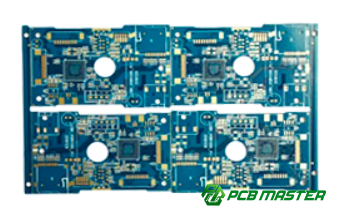
Multilayer PCB design refers to the process of creating printed circuit boards (PCBs) that contain more than two layers of conductive material (copper) separated by insulating layers (often made of fiberglass). These layers are stacked together and connected via vias, which are small conductive pathways that allow signals to travel between different layers.
Unlike single-layer or double-layer PCBs, which are limited in complexity and functionality, multilayer PCBs allow for more advanced designs. They enable smaller, more compact electronics by efficiently using the available space. This design allows for more routing space for signals, power distribution, and better overall performance.
Key Concept: The more layers a PCB has, the more complex and powerful it can be, supporting more circuits and features in a smaller space.
Multilayer PCBs in Modern Electronics
In today's electronics, multilayer PCBs are indispensable. They are used in a wide variety of devices, from smartphones and computers to medical equipment and automotive systems. As electronic devices become smaller, faster, and more feature-rich, multilayer PCBs are necessary to meet the growing demand for compact designs without sacrificing performance.
For instance, smartphones use multilayer PCBs to integrate various components like processors, memory, and power systems while keeping the device thin and lightweight. In contrast, older electronic devices with simpler functions often used single- or double-layer PCBs, limiting their performance and size.
The Apple iPhone relies on advanced multilayer PCBs to accommodate its complex features—such as high-speed processors, wireless communication modules, and power management—into its slim form factor.
Multilayer PCBs allow engineers to achieve higher component density, reduce electromagnetic interference (EMI), and improve signal integrity, all crucial for modern high-performance electronic devices. Their importance continues to grow as demand for more powerful and smaller electronics increases.
Key Challenges in Multilayer PCB Design
Key challenges in multilayer PCB design include managing complex layer stackups, ensuring signal integrity (such as crosstalk and impedance control), addressing thermal management issues, and avoiding common design rule violations.
Complex Layer Stackup Design
Designing the layer stackup is one of the most crucial and challenging tasks in multilayer PCB design. A stackup refers to how the different layers of a PCB are arranged, including signal, ground, and power layers. The complexity arises because the arrangement must ensure that electrical signals can travel without interference while maintaining the structural integrity of the board.
Challenge: The designer must consider factors like signal integrity, electromagnetic interference (EMI), and the mechanical strength of the board. The number of layers and their arrangement affect the overall performance of the PCB, especially for high-frequency applications like communication devices.
Solution: Designers must carefully plan the number of layers, their arrangement, and the materials used. For example, power and ground layers are often placed close to signal layers to reduce noise and maintain signal integrity. Specialized simulation software can help optimize the stackup and predict potential issues.
Real-World Example: In designing a high-speed network router, a carefully optimized stackup ensures minimal signal loss and interference, enabling fast data transmission between components.
Signal Integrity Management (Crosstalk, Impedance Control)
Signal integrity is critical in multilayer PCBs, especially for high-speed circuits where even small disturbances can cause errors. Crosstalk, which occurs when signals from one trace interfere with another, and impedance mismatches can lead to data corruption or poor performance.
Challenge: Ensuring signals maintain their strength and clarity is difficult due to the number of layers and the complexity of routing signals across different layers. Mismatched impedance can cause reflections, which distort signals, especially in high-frequency designs.
Solution: Impedance control is a technique that ensures all traces have a consistent impedance value, typically 50 ohms for signal traces. This helps prevent signal reflections. Additionally, careful routing and the use of ground planes between layers reduce the risk of crosstalk.
Real-World Example: In high-performance graphics cards, designers use controlled impedance traces to ensure that high-speed data is transmitted without loss, ensuring smooth video rendering and faster performance.
Thermal Management Challenges
Multilayer PCBs, especially in high-power applications, generate heat that can degrade performance and cause failures if not properly managed. Managing heat is especially challenging in compact designs where space for heat dissipation is limited.
Challenge: Heat can accumulate in components or traces, leading to thermal stress, which may cause material degradation or even failure. This issue is exacerbated when high-power components are placed in close proximity on a multilayer PCB.
Solution: Designers use heat sinks, thermal vias, and copper pours to help dissipate heat more effectively. Thermal simulation tools can predict where heat will build up, allowing designers to adjust the layout accordingly to ensure better thermal performance.
Real-World Example: In power amplifiers for telecommunications, designers often use copper pours and heat sinks to manage the heat generated by high-power transistors, preventing the PCB from overheating and ensuring long-term reliability.
Common Design Rule Violations and Their Solutions
Design rule violations can lead to manufacturing defects, performance issues, and failed designs. These violations often occur when PCB layouts don't adhere to the minimum spacing, trace width, or via size required by the manufacturing process.
Challenge: Ensuring that every aspect of the PCB layout follows strict design rules, such as trace width and spacing, is critical to ensure manufacturability and functionality. Violating these rules can result in short circuits, signal loss, or weak mechanical bonding between layers.
Solution: Utilizing Design for Manufacturability (DFM) tools can help detect and correct potential violations early in the design process. These tools check the layout against the manufacturer’s specifications and suggest changes to avoid errors.
Real-World Example: During the design of a consumer electronics device, a DFM tool might alert the designer that the vias are too small, which could lead to poor electrical contact. The designer can then adjust the design to ensure the vias meet the required standards.
How to Plan Your Multilayer PCB Layer Stackup
How to Design a Proper Layer Stackup
Designing a proper layer stackup involves arranging multiple layers of conductive (copper) and insulating materials to meet the electrical and mechanical requirements of your PCB. The stackup design depends on the application, the number of layers, and the need for signal integrity and power management.
Step-by-Step Process:
1. Determine the Number of Layers: Start by assessing the complexity of your design. High-speed or high-density circuits will need more layers.
2. Plan Signal and Power Layers: Allocate separate layers for power and ground, and keep signal layers as isolated as possible to reduce noise.
3. Optimize for Signal Integrity: Place ground and power layers adjacent to signal layers for better shielding and to prevent signal interference.
Common Material Choices and Layer Configuration
Choosing the right materials and configuring the layers appropriately is vital for achieving the desired performance, thermal management, and manufacturability of your PCB. Common materials include FR-4 for general use, while high-frequency designs may use materials like Rogers or PTFE for better signal transmission at higher speeds.
Material Examples:
l FR-4: A widely used, cost-effective material for most applications.
l Rogers: Used for high-frequency designs, offering better performance at higher speeds.
l PTFE: Known for low loss and high-frequency performance, often used in advanced RF applications.
Layer Configuration: A typical multilayer PCB might include alternating signal layers and power/ground layers. A balanced configuration can look like this:
l Signal
l Ground
l Signal
l Power
l Signal
l Ground
l Signal
This configuration helps minimize crosstalk and signal degradation.
Signal, Ground, and Power Plane Optimization Techniques
Optimizing the signal, ground, and power planes in a multilayer PCB design is critical for ensuring reliable performance, especially at high frequencies. These planes play a key role in managing signal integrity and power distribution, reducing noise, and controlling electromagnetic interference (EMI).
Optimization Techniques:
1. Use Ground Planes for Shielding: Place a dedicated ground plane close to signal layers to act as a shield, reducing the risk of interference.
2. Power Plane Allocation: Ensure power planes are thick enough to handle current without excessive voltage drop. Use copper pours to create large, continuous power and ground planes for better current distribution.
3. Use Vias for Connection: Vias are used to connect different layers. For power and ground layers, it's important to use a sufficient number of vias to reduce resistance and improve power delivery.
Real-World Example: In designing a high-speed data communication board, placing the ground plane adjacent to signal layers minimizes noise, ensuring that signals are transmitted cleanly and without distortion. This is critical in applications like 5G devices, where signal integrity is paramount.
Best Practices for Signal Integrity and Thermal Management
Best practices for signal integrity and thermal management include optimizing signal routing to reduce noise and crosstalk, using copper pours and heat sinks for effective heat dissipation, and employing thermal simulation tools to predict and manage heat distribution.
How to Optimize Signal Integrity: Reducing Crosstalk and Noise
Signal integrity is critical in multilayer PCB design, especially for high-speed circuits. Crosstalk (interference between signals) and noise can disrupt communication between components, leading to errors or malfunctions.
Key Optimization Techniques:
1. Use Ground Planes: Placing a continuous ground plane between signal layers helps shield signals from interference.
2. Maintain Proper Trace Spacing: Ensuring adequate spacing between traces reduces the chances of crosstalk.
3. Controlled Impedance: Design traces with consistent impedance to avoid signal reflections and losses, especially important for high-speed circuits.
4. Use Differential Pair Routing: For high-frequency signals, use differential pair routing where two traces carry opposite signals, helping cancel out noise.
Real-World Example: In high-speed network routers, careful trace routing and grounding techniques help maintain clear data transmission without interference, ensuring reliable communication.
Basic Thermal Management Strategies: Copper Pours, Heat Sinks, and Component Layout
Effective thermal management is crucial to prevent overheating and ensure the long-term reliability of multilayer PCBs. Overheating can cause components to fail or degrade in performance, especially in high-power applications.
Thermal Management Techniques:
l Copper Pours: Copper pours act as a large heat sink on the PCB, helping to distribute and dissipate heat more efficiently.
l Heat Sinks: Attaching heat sinks to power-hungry components (like processors or voltage regulators) helps to absorb and dissipate heat away from the PCB.
l Component Placement: Arrange high-power components in areas with better airflow or near heat-dissipating elements to minimize heat buildup.
Real-World Example: In a power supply unit for an electric vehicle, copper pours and strategically placed heat sinks prevent overheating of critical power regulation components, ensuring the system runs efficiently and safely.
Thermal Analysis and Simulation Tools
Thermal analysis and simulation tools allow designers to predict how heat will behave in a PCB design and make adjustments before physical production. These tools can help avoid thermal issues that might not be apparent through simple design inspection.
Thermal Simulation Tools:
l ANSYS Icepak: A popular thermal simulation tool that helps model and analyze heat flow in electronic components.
l SolidWorks Flow Simulation: Used to simulate airflow and thermal distribution within a PCB design to prevent overheating.
l CFD Tools: Computational Fluid Dynamics (CFD) tools help simulate how air moves around components, assisting in designing efficient cooling strategies.
Real-World Example: Before manufacturing a new smartphone, designers use thermal analysis tools to identify potential hotspots around the processor and battery. They then adjust the layout and add additional copper pours or heat sinks to ensure the device stays cool during use.
Tools for Efficient Multilayer PCB Design
Efficient multilayer PCB design requires using powerful tools like Altium Designer, Eagle, and KiCad for layout, along with signal integrity and thermal analysis tools, and DFM tools to ensure manufacturability and optimal performance.
Recommended PCB Design Software: Altium Designer, Eagle, KiCad
Designing a multilayer PCB requires the right software tools to ensure accuracy, efficiency, and manufacturability. There are several PCB design tools available, but Altium Designer, Eagle, and KiCad are some of the most popular options used by engineers.
l Altium Designer: Known for its advanced features, Altium Designer is highly favored in industries that require complex designs. It offers a powerful schematic capture tool, PCB layout editor, and simulation capabilities. Its intuitive interface makes it easy to design high-performance multilayer PCBs.
l Eagle: A cost-effective solution for hobbyists and small businesses, Eagle offers a robust set of tools for PCB design, including schematic capture and layout editing. It’s popular for its user-friendly interface and flexibility, with a wide range of libraries for components.
l KiCad: This open-source tool is free and offers powerful features that rival commercial options. KiCad includes schematic capture, PCB layout, and a 3D viewer to visualize the design. It’s ideal for engineers looking for a robust tool without a high cost.
Real-World Example: A small startup designing a smart home device may choose Eagle for its cost-efficiency and ease of use, while a large company developing advanced medical equipment may opt for Altium Designer to take advantage of its higher-end simulation and design capabilities.
Signal Integrity and Thermal Analysis Tools
For efficient multilayer PCB design, it’s essential to ensure that the signals flow smoothly and the board doesn’t overheat. Signal integrity and thermal analysis tools help engineers analyze and optimize their designs for performance and reliability.
l Signal Integrity Tools: These tools analyze high-speed signals, detecting issues like crosstalk, reflections, and impedance mismatches. Examples include HyperLynx (for signal integrity analysis) and SIwave (for modeling high-speed circuits).
l Thermal Analysis Tools: These tools help simulate how heat will flow through the PCB design, identifying potential hotspots and areas where heat dissipation could be improved. Tools like ANSYS Icepak and SolidWorks Flow Simulation provide in-depth thermal analysis to avoid overheating.
Real-World Example: A company designing a gaming PC uses thermal analysis tools to ensure the processor and GPU remain cool under load, preventing overheating that could lead to system crashes.
How to Use DFM (Design for Manufacturability) Tools to Improve Design Efficiency
DFM tools are essential for improving the manufacturability of your PCB design. These tools help ensure that your design adheres to manufacturing constraints, such as trace width, spacing, and via size, which can reduce production costs and errors.
l Key DFM Features: DFM tools check for violations in design rules like trace width, via size, and spacing. They also flag issues related to component placement and layer count, ensuring that your design can be efficiently produced with minimal errors.
l Popular DFM Tools: Mentor Graphics Valor, Zuken DFM, and Cadence Allegro are popular DFM tools that automatically check for design violations. These tools not only highlight issues but also provide solutions to correct them before production begins.
Real-World Example: Before sending a PCB design to a manufacturer, a company uses DFM tools to check for trace width violations, which helps avoid costly fixes during manufacturing and ensures the board is optimized for assembly.
How to Address Common Multilayer PCB Design Failures
To address common multilayer PCB design failures, such as delamination and signal attenuation, ensure proper layer bonding, use impedance control, and perform thorough functional, thermal, and electrical testing during the design phase.
Common Failure Modes and Troubleshooting: Delamination, Signal Attenuation
Multilayer PCBs can experience various failures, such as delamination and signal attenuation, which can lead to functionality issues or complete device failure.
l Delamination: This failure happens when the layers of the PCB, which are bonded together, begin to separate due to poor adhesion, moisture, or thermal stress. It is most common in high-temperature environments or with poor manufacturing processes. To address this, ensure high-quality materials are used and that the PCB undergoes proper thermal cycling tests during production.
l Signal Attenuation: As electrical signals travel across the PCB, their strength can decrease due to resistance and other factors, particularly in high-frequency applications. To minimize this, use proper impedance control, minimize trace lengths, and optimize layer stackup to ensure signal paths are clear and consistent.
Real-World Example: A consumer electronics manufacturer experiences poor signal quality in a new device. After troubleshooting, it is found that signal attenuation was caused by overly long signal traces and insufficient ground plane coverage, which were rectified by redesigning the PCB layout.
Design Debugging and Testing Methods: Ensuring Functionality and Reliability
To ensure that a multilayer PCB works correctly and reliably, thorough testing and debugging are necessary at each stage of the design process. This helps identify potential failures early on, reducing the risk of issues after manufacturing.
l Functional Testing: After completing the design, functional tests check if the PCB operates as intended in real-world conditions. This includes testing for voltage, current, and signal integrity. It ensures that each circuit performs its job correctly and that no component is malfunctioning.
l Thermal Testing: Overheating is a common issue in multilayer PCBs, particularly in power-intensive applications. Thermal cameras or simulation tools (like ANSYS Icepak) can identify hot spots where heat may be building up. This helps ensure that the design includes sufficient cooling measures, like heat sinks or copper pours.
l Electrical Testing: This method ensures that there are no short circuits, opens, or improper connections in the PCB. Tools like Automatic Test Equipment (ATE) or Boundary Scan are commonly used to check for electrical faults in complex designs.
Real-World Example: A company designing a high-performance medical device uses thermal and functional testing to ensure that the PCB does not overheat or cause electrical failure under load. These tests help identify a weak connection in a critical component, which is fixed before production.
Conclusion
In the world of multilayer PCB design, ensuring optimal performance and reliability requires careful attention to detail, from planning the stackup and managing signal integrity to addressing thermal challenges. By following best practices, using the right tools, and testing thoroughly, you can avoid common design failures and create high-quality, efficient PCBs.
For those looking for reliable and high-performance PCB solutions, partnering with a trusted supplier can make all the difference. PCBMASTER, a seasoned PCB and PCBA provider, is dedicated to offering top-tier products, including advanced multilayer PCBs, that meet the highest industry standards. With their expertise and commitment to quality, PCBMASTER ensures that every design is built to perform, no matter the complexity.
FAQs About Multilayer PCB Design
1. How many layers should a multilayer PCB have?
The number of layers in a multilayer PCB depends on the complexity and requirements of the design. Common multilayer PCBs have 4 to 12 layers, but high-performance applications can have up to 32 layers or more. The layers are chosen based on factors such as signal routing, power distribution, and the need for compact designs.
2. What is the best material for a multilayer PCB?
The best material for a multilayer PCB typically depends on the application. FR4 (fiberglass-reinforced epoxy) is the most commonly used material due to its balance of cost, durability, and performance. For high-frequency applications, materials like Rogers or PTFE are preferred because they have lower dielectric constants and are better for signal integrity.
3. How do I reduce thermal issues in multilayer PCBs?
To reduce thermal issues in multilayer PCBs:
l Use copper pours to spread heat across the board.
l Copper thickness should be chosen carefully to enhance heat dissipation.
l Place heat sinks on high-power components.
l Ensure proper layer stackup, with ground and power layers close to signal layers.
l Use thermal vias to transfer heat to other layers.
Perform thermal simulation during the design phase to identify hot spots.
4. What are the common design mistakes to avoid?
Common design mistakes to avoid include:
l Improper layer stackup, which can lead to signal integrity issues.
l Insufficient power and ground planes, leading to voltage drops and noise.
l Trace width and spacing errors, causing manufacturing issues or signal interference.
l Ignoring thermal management, which can cause overheating and component failure.
l Failure to check DFM (Design for Manufacturability), resulting in designs that are difficult or expensive to produce.
These best practices can help ensure that your multilayer PCB designs are efficient, reliable, and cost-effective.

