


What Causes Copper Void Issues in PCB Holes and How to Fix Them?
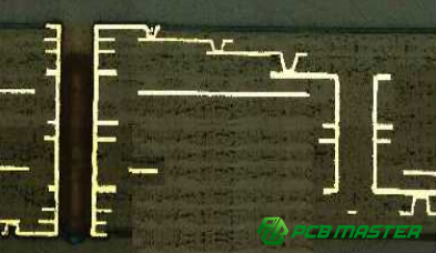
Copper voids or hollow walls in PCB (Printed Circuit Board) manufacturing refer to areas where the copper plating fails to properly coat the walls of holes in the board. This issue can cause weak electrical connections, leading to poor performance or even complete failure of the circuit. Copper voids are particularly problematic in high-density designs, where precise and reliable connections are crucial.
These defects typically occur during the copper plating process, when the copper fails to uniformly coat the hole walls. This can happen due to poor hole preparation, chemical imbalances, or issues during the electroplating phase. For manufacturers, these voids can result in costly repairs, production delays, and quality control challenges.
The article will explore the main causes of copper voids in PCB manufacturing (ranging from drilling problems to plating issues), offering a step-by-step guide to diagnosing and addressing the issue.
What Drilling Issues Can Lead to Copper Voids in PCB Holes?
Drilling issues such as worn drill bits, mismatched drilling speeds and feed rates, and contamination from oil, dust, or drill shavings can prevent proper copper plating, leading to copper voids in PCB holes.
1. Incorrect Drilling Machine Parameters
Drill Bit Wear:
When drill bits become worn out, they no longer create smooth, clean holes. The edges of a dull drill bit may cause rough surfaces or uneven walls inside the hole. These imperfections prevent the copper from adhering properly during the plating process, which can lead to voids or hollow areas where copper should have deposited. Regular maintenance and timely replacement of drill bits are essential to avoid these issues and ensure that the copper plating process works smoothly.
Mismatch Between Speed and Feed Rates:
Drill speed (how fast the drill bit spins) and feed rate (how fast the drill bit moves into the material) must be correctly matched for optimal drilling. If the speed is too high for the feed rate, it can cause excessive heat and friction, damaging the hole's walls and creating an uneven surface. On the other hand, a low feed rate with high speed can lead to poorly drilled holes with jagged edges, which also interferes with proper copper adhesion. To avoid these issues, it’s important to adjust the machine settings according to the material type and hole size.
2. Hole Wall Contamination
Oil, Dust, or Drill Shavings Residue:
After drilling, small particles like oil, dust, and shavings from the drill bit can remain inside the hole. These residues create a barrier that prevents the chemical solutions from effectively contacting the hole walls. In the copper plating process, this contamination prevents the copper from bonding with the PCB material. A thorough cleaning step, including ultrasonic cleaning or other specialized methods, is essential to remove these contaminants and ensure a clean surface for plating. If not properly cleaned, even the best chemical solutions will struggle to form a strong bond, leading to copper voids.
By addressing these drilling-related issues, manufacturers can significantly reduce the likelihood of copper voids in PCBs, ensuring a stronger and more reliable final product.
What Issues Can Arise During the Chemical Copper Plating Process?
Issues during the chemical copper plating process, such as incomplete resin removal, insufficient activation, and imbalanced chemical solutions, can lead to poor copper adhesion, resulting in voids or hollow areas in the PCB holes.
1. Incomplete Removal of Resin Residues
Why are High-TG and Halogen-Free Boards More Likely to Have Incomplete Resin Removal?
High-TG (glass transition) boards and halogen-free boards use materials that are more resistant to oxidation. These materials are harder to treat during the chemical copper process, especially when it comes to removing resin residues from the holes. If these residues aren’t completely removed, they form a barrier that prevents the copper from properly bonding to the hole walls. Incomplete resin removal leads to poor copper deposition and results in voids or hollow spots. To solve this, manufacturers may need to adjust the cleaning and treatment steps for these special materials, using stronger or more effective chemicals.
2. Poor Activation
How Does Insufficient Activation Liquid Activity Affect Copper Deposition?
Activation is a critical step where a thin layer of catalyst is applied to the hole walls to promote copper adhesion. If the activation liquid doesn't have enough activity (due to low concentration or improper formulation), it can’t effectively create the necessary catalytic layer on the PCB. This means copper won’t bond well with the surface, leading to incomplete copper plating and possible voids. It’s crucial to monitor and maintain the correct chemical balance to ensure that the activation process works as intended.
How Does Poor Hydrophilicity of the Hole Walls Block Activation Liquid Penetration?
Hydrophilicity refers to how well the surface attracts water. If the hole walls are hydrophobic (repelling water), the activation liquid will struggle to penetrate deep into the holes, especially in high aspect ratio holes (holes that are deeper than their diameter). Without proper activation inside the entire hole, copper cannot effectively deposit, leaving parts of the hole without copper plating. This issue can be avoided by improving the surface treatment and ensuring the activation liquid reaches the entire hole.
3. Chemical Copper Deposition Failure
How Do Chemical Solution Imbalances Affect Copper Deposition?
Chemical copper deposition relies on a precise balance of chemicals, including copper ions (Cu²⁺), formaldehyde, pH levels, and temperature. If these elements are not properly maintained—such as when the copper ion concentration is too low, formaldehyde is imbalanced, or the temperature is incorrect—the copper plating process fails. The result is insufficient copper coverage, which can cause weak electrical connections or empty spots where copper should be present. Manufacturers should carefully monitor and adjust these parameters for optimal plating results.
How Does Poor Chemical Exchange Within the Hole Affect Copper Deposition?
In high aspect ratio holes, the copper solution must circulate properly inside the hole to deposit copper evenly on the walls. If the solution doesn’t flow or exchange well (due to poor agitation or insufficient circulation), the copper plating will not be uniform. This issue is especially prominent in small, deep holes where the chemical reaction can become limited in the middle of the hole, leaving the bottom or deeper parts with no copper. Ensuring adequate agitation and circulation of the solution is crucial to achieve even copper deposition.
By addressing these chemical plating issues, manufacturers can significantly reduce the occurrence of copper voids and achieve higher quality, more reliable PCBs.
What Issues Can Arise During the Electroplating Process?
Issues during the electroplating process, such as poor pre-treatment, incorrect current density, imbalanced solution composition, inadequate agitation, and solution contamination, can lead to uneven copper plating and voids in PCB holes.
1. Poor Pre-Electroplating Treatment
How Does Oxidation or Contamination of the Chemical Copper Layer Affect Subsequent Electroplating?
Before electroplating, the PCB is coated with a thin layer of chemical copper. If this layer becomes oxidized or contaminated, it can prevent the electroplating copper from adhering properly. Oxidation forms a barrier that blocks copper deposition, while contaminants like dust or oil can also create uneven surfaces. This results in poor adhesion and leads to copper voids or weak spots in the final product. To avoid this, manufacturers must ensure proper cleaning and treatment of the chemical copper layer before starting the electroplating process.
2. Electroplating Parameter and Equipment Issues
How Does High or Low Current Density Cause Uneven Copper Plating?
Current density refers to the amount of electrical current applied to the PCB during electroplating. If the current density is too high, the copper will deposit too quickly at the edges of the hole, causing "crowning" or thick copper layers at the hole entrance. If the current density is too low, the copper will deposit too slowly, leading to thin copper layers, particularly in the deeper parts of the hole. Both situations create uneven plating and copper voids. The key is to maintain the correct current density for uniform copper distribution.
How Can Abnormal Electroplating Solution Composition Affect Copper Plating?
The electroplating solution needs to have a precise balance of copper ions, sulfuric acid, and additives. If any of these components are too concentrated or out of balance, it can cause poor plating quality. For example, too few copper ions will result in weak plating, while too much sulfuric acid can damage the copper layer. Additives like brighteners and leveling agents also need to be in the right proportions to ensure smooth, even copper deposition. Regular monitoring and adjustment of the plating solution are necessary for consistent results.
How Does Insufficient Agitation or Circulation Affect Copper Plating?
Proper agitation or circulation of the electroplating solution is essential to ensure even copper coverage. If the solution doesn’t circulate well, parts of the PCB, especially the deeper holes, will not receive enough copper. This can cause incomplete plating and result in copper voids. Agitation helps prevent the buildup of gas bubbles, which can also interfere with the copper deposition process. Proper fluid flow ensures that the copper ions are evenly distributed across the entire surface, leading to a uniform plating.
3. Electroplating Solution Contamination
How Does Organic or Metal Ion Contamination Affect Copper Plating Quality?
Contaminants in the electroplating solution, such as organic material or unwanted metal ions, can severely affect the quality of the copper plating. Organic contaminants can prevent the copper from adhering uniformly, leading to rough or incomplete plating. Metal ions from previous plating runs or environmental sources can cause the formation of defects like pits or irregular copper layers. To maintain plating quality, it is crucial to regularly filter and clean the electroplating solution to remove any contaminants.

How Do Material and Environmental Factors Affect Copper Deposition on PCB Hole Walls?
Material and environmental factors, such as incomplete dry film development, residual solder mask, workshop dust, and poor water quality, can create barriers or disrupt the chemical plating process, leading to uneven or incomplete copper deposition on PCB hole walls.
1. Impact of Dry Film or Solder Mask
How Does Incomplete Development or Residual Film Affect Copper Layer Adhesion?
In PCB manufacturing, a dry film or solder mask is often used to protect parts of the PCB from unwanted copper deposition. However, if the dry film is not properly developed or if residual film remains on the PCB, it can create areas that are insulated and prevent copper from adhering to those parts of the hole walls. This insulation can block the copper plating process, resulting in voids or gaps in the copper layer. To ensure proper adhesion, it’s critical to clean the PCB thoroughly after developing the dry film and remove any remaining mask material before proceeding with copper plating.
2. Environmental and Water Quality Factors
How Does Workshop Dust and Pollution Contaminate Plating Solution and Plating Process?
In PCB manufacturing environments, dust, dirt, and other pollutants can easily contaminate the plating solutions used in copper deposition. These contaminants can enter the holes and stick to the walls of the PCB, creating a barrier between the chemical solution and the material. As a result, the copper deposition process becomes inconsistent, leading to incomplete or uneven plating. Proper cleanliness in the workshop, including air filtration systems and regular cleaning of tools, is essential to prevent contamination that could impact copper layer quality.
How Does Poor Water Quality Affect Chemical Solution Stability and Copper Deposition?
Water quality is crucial for maintaining the stability of the chemicals used in the copper plating process. Hard water or water with high levels of minerals can alter the chemical composition of the plating solution, affecting its ability to properly deposit copper. Additionally, poor water quality can cause the plating solution to become unstable, leading to inconsistent copper layers or incomplete plating. It’s important to use filtered or purified water in the plating process and regularly test water quality to ensure that it does not interfere with the copper deposition process.
By addressing these material and environmental factors, manufacturers can improve the consistency and quality of copper plating on PCB hole walls, minimizing defects like voids and ensuring a more reliable final product.
What Role Do Design Factors Play in Copper Voids in PCB Hole Walls?
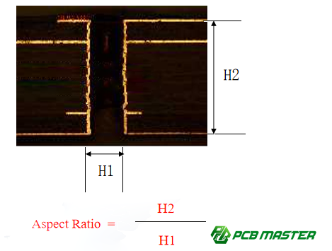
Design factors like a high aspect ratio (large board thickness-to-hole diameter ratio) and uneven or dense hole spacing can hinder proper copper deposition, leading to copper voids or uneven plating in PCB hole walls.
1. Large Aspect Ratio of Holes
How Does a High Board Thickness-to-Hole Diameter Ratio Affect Chemical Copper Deposition and Electroplating Difficulty?
A high aspect ratio in PCB design refers to a situation where the hole depth is much greater than the hole diameter. When the thickness of the PCB is large relative to the hole size, it becomes much harder for both chemical copper deposition and electroplating to cover the entire surface of the hole, especially in deep or narrow holes. This is because the chemicals or plating solution have difficulty reaching the deeper sections of the hole, leading to incomplete copper deposition, particularly in the center or bottom of the hole. As a result, copper voids or hollow areas can form. To avoid these issues, designs should aim to keep the aspect ratio within manageable limits, or manufacturers should optimize their plating techniques to handle deeper holes.
2. Dense or Uneven Hole Spacing
How Does Uneven Hole Spacing Lead to Uneven Current Distribution and Copper Plating?
When holes in a PCB are placed too close together or are unevenly spaced, it can affect the way current flows during electroplating. In areas where holes are very close, the electrical current tends to concentrate at the edges of the holes, leading to thicker copper deposits around the hole entrances and thinner layers deeper inside the hole. This uneven current distribution results in inconsistent copper plating, with some areas of the hole wall being inadequately covered or left without copper. Proper hole spacing and even distribution across the PCB layout can help achieve uniform copper deposition and reduce the likelihood of copper voids or gaps in the hole walls.
By carefully considering hole aspect ratios and spacing during the PCB design process, manufacturers can minimize the risk of copper voids, ensuring better electrical performance and reliability in the final product.
How to Prevent and Resolve Copper Voids in PCB Hole Walls?
To prevent and resolve copper voids in PCB hole walls, systematically diagnose issues across the entire production process and optimize drilling quality, equipment maintenance, and chemical copper deposition and electroplating parameters.
1. Diagnosis and Troubleshooting
How to Conduct a Systematic Diagnosis to Identify the Source of the Problem?
To effectively prevent and resolve copper voids in PCB hole walls, it is essential to carry out a systematic inspection across the entire manufacturing process, from drilling to electroplating. Start by examining the drilling phase for issues like worn drill bits or improper drill speed, as these can create rough hole surfaces. Next, check the cleaning and activation processes to ensure that no contamination or incomplete resin removal is blocking copper adhesion. During electroplating, monitor the current density, solution composition, and agitation to ensure uniform copper deposition. By identifying and addressing issues at each stage, manufacturers can pinpoint the exact cause of copper voids and implement targeted solutions. Regular audits and inspections throughout production help maintain high-quality standards.
2. Optimizing Production Processes
How to Improve Drilling Quality and Equipment Maintenance?
One of the key factors in preventing copper voids is ensuring that the drilling process is precise and efficient. This involves using high-quality drill bits and ensuring they are regularly maintained or replaced to avoid wear. It’s also crucial to fine-tune drilling parameters, such as speed and feed rate, to match the material and hole size. For example, drilling too fast or with a dull bit can create rough hole walls, which make it difficult for copper to adhere during plating. Regular maintenance of drilling machines and continuous monitoring of drill conditions can significantly reduce these issues and improve overall hole quality.
How to Optimize Chemical Copper Deposition and Electroplating Processes?
To prevent copper voids, the chemical copper deposition and electroplating processes must be optimized. Adjusting the chemical solution's composition, temperature, and pH level ensures consistent copper plating. For instance, balancing copper ion concentration and formaldehyde levels in the chemical copper bath prevents improper copper adhesion. Additionally, controlling electroplating parameters, such as current density, is crucial for ensuring uniform copper deposition throughout the holes. Agitation of the plating solution is another key factor; it helps maintain an even flow of the chemical solution inside the holes, ensuring that deep holes receive adequate copper coverage. By fine-tuning these factors, manufacturers can minimize the likelihood of copper voids.
By systematically diagnosing issues and optimizing both drilling and plating processes, manufacturers can effectively prevent and resolve copper voids, ensuring high-quality, reliable PCBs.
Conclusion
Avoiding copper voids in PCB hole walls requires a thorough approach, starting with systematic troubleshooting across the entire manufacturing process, from drilling to electroplating. By addressing issues at each stage—such as ensuring proper hole preparation, maintaining correct chemical composition, and optimizing electroplating parameters—manufacturers can significantly reduce the occurrence of voids. Additionally, continuous monitoring and process optimization are essential for maintaining high-quality standards and ensuring consistent results.
When it comes to reliable and high-quality PCBs, PCBMASTER stands out as a seasoned PCB and PCBA supplier. With years of experience and a commitment to excellence, PCBMASTER ensures that every product undergoes rigorous quality control to eliminate issues like copper voids, delivering top-notch results to customers. Their expertise and attention to detail guarantee that users receive only the best, free from common PCB manufacturing defects.
FAQs
Why are high TG materials more prone to copper voids in PCB holes?
High TG materials have resins that are difficult to oxidize, which leads to incomplete resin removal during the chemical copper process. This incomplete cleaning prevents proper copper deposition, resulting in copper voids or gaps in the hole walls.
How can you identify current density issues during electroplating?
If the copper layer at the hole entrance is much thicker than the copper inside the hole, it could indicate uneven current density. This imbalance causes excessive copper deposition at the hole's entrance and insufficient plating in the deeper areas, resulting in copper voids.
How can dense hole spacing lead to copper voids?
When holes are spaced too closely together, the electric current during electroplating can become unevenly distributed. This leads to poor copper coverage, particularly in smaller or deeper holes, causing copper voids in the areas that are not sufficiently plated.
How does electroplating solution contamination affect copper plating on hole walls?
Organic or metal ion contamination in the electroplating solution can interfere with the uniform deposition of copper. These contaminants create uneven plating, leading to localized voids or areas where copper is completely absent.
How can you address the root cause of copper voids in PCB holes?
The fundamental solution is to conduct a thorough, step-by-step diagnosis of the entire process, from drilling to chemical copper deposition and electroplating. By optimizing each process and ensuring strict quality control at every stage, manufacturers can prevent copper voids and ensure consistent quality.
Author Bio
Hi, I'm Carol, the Overseas Marketing Manager at PCBMASTER, where I focus on expanding international markets and researching PCB and PCBA solutions. Since 2020, I've been deeply involved in helping our company collaborate with global clients, addressing their technical and production needs in the PCB and PCBA sectors. Over these years, I've gained extensive experience and developed a deeper understanding of industry trends, challenges, and technological innovations.
Outside of work, I'm passionate about writing and enjoy sharing industry insights, market developments, and practical tips through my blog. I hope my posts can help you better understand the PCB and PCBA industries and maybe even offer some valuable takeaways. Of course, if you have any thoughts or questions, feel free to leave a comment below—I'd love to hear from you and discuss further!

