


Back Drill Deep Control in PCB Manufacturing: Enhancing Signal Integrity and Reducing Crosstalk
The performance of modern electronic devices hinges on the reliability and speed of their underlying Printed Circuit Boards (PCBs). As technology advances, signal integrity has become a top priority, especially for high-speed, multi-layer PCB designs. One of the most effective techniques for optimizing signal transmission and reducing interference is Back Drill Deep Control. This method addresses the challenges of unwanted crosstalk and signal degradation by precisely managing the depth of drilled holes in the PCB.
As electronic components become smaller and more intricate, even minor disruptions in signal flow can lead to significant performance issues. Back drill deep control provides a solution by removing excess copper from vias, ensuring smoother signal paths and reducing electromagnetic interference.
Let's dive into the process, exploring what back drill deep control is, why it's crucial for maintaining signal integrity, and how it significantly reduces crosstalk in multi-layer PCBs.
What is Back Drill Deep Control in PCB Manufacturing?
Back Drill Deep Control in PCB manufacturing is a process that precisely removes excess copper from vias on the backside of the PCB to improve signal integrity and reduce interference, especially in high-speed or high-frequency designs.
Defining Back Drilling and Deep Control
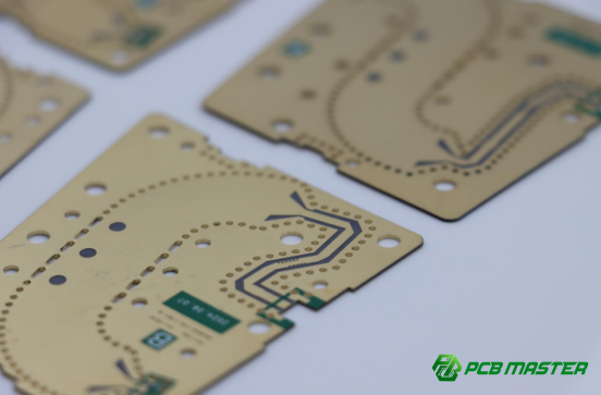
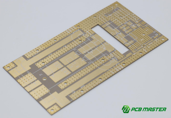
Back drilling is a process in PCB manufacturing where holes (vias) are drilled from the backside of the PCB to remove excess copper that is not part of the signal path. This copper is typically leftover from vias that connect different layers of the PCB. In high-frequency or high-speed designs, any excess copper can act as an antenna or cause unwanted interference.
Deep control refers to the precise management of the drilling depth. The goal is to ensure that only the unnecessary copper is removed, leaving the essential parts of the PCB intact. This controlled depth helps to fine-tune the electrical characteristics of the PCB, which is critical for high-speed signals. Deep control ensures that the holes are drilled accurately without damaging the board or affecting the performance of the circuit.
The Process: Step-by-Step Overview of How Back Drilling Works
1. Design Phase: Engineers identify which vias need back drilling based on the PCB design, particularly those that could impact signal integrity due to excess copper.
2. Drilling Setup: Special equipment is set up to drill from the backside of the board. The depth and diameter of the drill are carefully controlled to remove only the unwanted copper.
3. Drilling Execution: The machine drills the vias, ensuring that only the excess copper is removed and the desired depth is maintained.
4. Inspection and Quality Control: After drilling, the PCB undergoes inspection, often using methods like X-ray to confirm that the drill depth is correct and no damage has occurred to the board.
This step-by-step process ensures that the PCB performs at its best by removing interference-causing materials without compromising its structural integrity.
Why is Back Drill Deep Control Necessary?
Back drill deep control is crucial for improving the performance of PCBs, especially in high-frequency and high-speed applications. Here's why:
The Role of Back Drilling in High-Frequency PCB Designs
In high-frequency PCBs, such as those used in telecommunications or advanced computing, signals travel at very high speeds. Even small amounts of interference, such as those from excess copper in vias, can significantly degrade signal quality. Back drilling helps to remove this excess copper, ensuring that signals flow smoothly without distortion. By removing unwanted conductive material, back drilling ensures that the PCB operates effectively in high-speed environments.
How Deep Control Prevents Unwanted Signal Reflections and Loss
When there is excess copper in vias, it can create unwanted electrical paths or reflections. These reflections occur when signals bounce off the copper, causing delays or distortions. By controlling the depth of back drilling, manufacturers ensure that only the necessary copper is left intact. This prevents signal loss, reflections, and the creation of unwanted paths that can interfere with the proper transmission of signals. In essence, deep control enhances the overall signal integrity by ensuring the via only supports the intended signal route.
For example, in high-speed digital circuits used in modern computers or smartphones, signal integrity is critical to prevent data errors. Back drill deep control ensures that signals do not encounter unexpected obstacles, resulting in faster, more reliable data transmission.
By applying back drill deep control, manufacturers can enhance the performance and longevity of PCBs, ensuring that electronic devices function reliably in demanding applications.
How Does Back Drill Deep Control Enhance Signal Integrity?
Back drill deep control enhances signal integrity by removing excess copper and unwanted vias from the PCB, preventing interference, signal reflections, and electromagnetic noise, leading to clearer and more reliable signal transmission.
The Importance of Signal Integrity in High-Speed PCBs
Signal integrity refers to the quality of the electrical signals as they travel through a PCB. In high-speed PCBs, which are commonly used in modern electronics like smartphones, computers, and communication devices, signal integrity is crucial because even tiny disruptions in the signal can cause big problems. When signals lose their clarity or strength, data can be corrupted, leading to errors, delays, or even system failures.
Poor signal integrity can result in several issues, including data loss or signal distortion, where the signal doesn't reach its destination correctly. In high-speed circuits, these problems are even more pronounced, as signals travel faster and are more prone to interference. For instance, in digital circuits, a corrupted signal can lead to incorrect data being processed, causing software crashes or malfunctions.
Therefore, ensuring signal integrity is a top priority when designing and manufacturing high-speed PCBs. Back drill deep control plays a critical role in achieving this by removing sources of interference and ensuring that signals pass through the board with minimal degradation.
How Back Drill Deep Control Improves Signal Integrity
Back drill deep control improves signal integrity by removing unwanted vias and excess copper traces that could otherwise cause signal degradation. These unwanted features act as obstacles to the signal, creating unwanted pathways or electrical noise that can interfere with the proper transmission of signals.
The process of back drilling involves drilling from the backside of the PCB to precisely remove the excess copper around the vias. This helps to eliminate the unwanted electrical paths that could distort or reflect the signal, leading to clearer, more reliable data transmission.
Additionally, back drill deep control helps prevent electromagnetic interference (EMI) and crosstalk. EMI is caused by electrical signals interfering with nearby components or traces, while crosstalk occurs when signals from one trace leak into adjacent traces. By removing excess copper, back drilling reduces the chance of these interferences, allowing signals to travel more freely without distortion.
Practical Examples of Signal Improvement Using Back Drill Deep Control
A real-world example of the benefits of back drill deep control can be seen in high-speed communication systems. In these systems, back drilling is used to remove excess copper from the vias, which significantly improves the quality of the signals traveling through the PCB. With the unwanted copper removed, the signals experience fewer delays and less distortion, leading to faster and more reliable communication.
For instance, in a PCB designed for a 5G mobile device, back drill deep control can be applied to minimize the interference caused by excess copper in vias. This results in clearer, faster data transfer with fewer errors, enhancing the overall performance of the device. Without back drilling, the excess copper could cause unwanted signal reflections, reducing the quality of the 5G signal and slowing down data transfer.
To further illustrate, let’s compare two PCBs—one with back drilling and one without. The PCB with back drilling shows a significant reduction in signal distortion, resulting in more accurate data transmission and faster processing times. In contrast, the PCB without back drilling experiences more signal loss and reflections, causing data errors and slower speeds. This comparison demonstrates the clear benefits of back drill deep control in maintaining signal integrity.
How Does Back Drill Deep Control Reduce Crosstalk in Multi-layer PCBs?
Back drill deep control reduces crosstalk in multi-layer PCBs by removing excess copper around vias, preventing unwanted capacitive and inductive coupling between layers and minimizing signal interference.
What is Crosstalk and How Does it Affect PCB Performance?
Crosstalk refers to the unwanted transfer of signals between adjacent traces or circuits within a PCB. This happens when the electromagnetic fields from one signal path induce a signal in a nearby path, causing interference. In high-speed or high-frequency PCBs, crosstalk leads to signal degradation, where the intended signal gets distorted or weakened due to interference from nearby signals. This can result in data errors, slower speeds, or complete malfunction in electronic systems.
In multi-layer PCBs, where many layers of circuits are stacked, crosstalk is particularly problematic. It occurs due to unwanted coupling between the layers. As the signals travel through these layers, the electromagnetic fields from one layer can affect the adjacent layers, causing interference. This is especially problematic in high-speed designs, where even the smallest amount of interference can lead to significant performance issues.
Back Drilling and Crosstalk Reduction
Back drilling plays a critical role in reducing crosstalk in multi-layer PCBs by removing excess copper around vias that could contribute to unwanted coupling. Vias are used to connect different layers of a PCB, but if not properly managed, they can create paths for interference. Excess copper around the via creates a conductive surface that can act as an antenna, picking up and transferring signals between nearby traces or layers.
By using back drill deep control, the unwanted copper around the via is precisely removed, leaving only the necessary portions intact. This reduces the chances of capacitive and inductive coupling between layers. Capacitive coupling occurs when the electric fields of adjacent traces interfere with each other, while inductive coupling happens when magnetic fields induce unwanted signals in nearby traces. By reducing the copper around the vias, back drilling minimizes both forms of coupling, improving overall signal integrity and reducing crosstalk.
Real-World Examples of Crosstalk Reduction
A practical example of how back drill deep control reduces crosstalk can be observed in high-speed digital systems, such as 5G communication devices. In these devices, back drilling is used to eliminate the excess copper from vias that could otherwise cause interference between signal paths. This results in clearer, faster data transmission with significantly fewer errors.
To illustrate, let’s compare two PCBs: one with back drilling and one without. The PCB without back drilling exhibits high levels of crosstalk, which leads to signal distortion and slower data transfer rates. In contrast, the PCB with back drilling shows dramatically reduced crosstalk, allowing signals to travel more freely and with higher accuracy. This comparison highlights the real-world benefits of back drilling in minimizing interference and improving the performance of high-speed, multi-layer PCBs.
Conclusion
In today's electronics industry, ensuring high signal integrity and minimizing crosstalk are crucial for the performance of high-speed, multi-layer PCBs. Through techniques like back drill deep control, manufacturers can precisely remove excess copper, improving signal quality and reducing unwanted interference. This process is essential for optimizing the performance of PCBs, especially in demanding applications like telecommunications and high-frequency devices.
As a trusted PCB supplier, PCBMASTER understands the importance of maintaining high standards in PCB manufacturing. With years of expertise, PCBMASTER employs strict processes to ensure effective back drill deep control, resulting in high-quality PCBs that guarantee superior signal integrity and minimal interference. By focusing on these advanced manufacturing techniques, PCBMASTER is committed to providing reliable solutions that meet the needs of its customers, ensuring optimal performance for a wide range of electronic applications.
FAQs
What is the difference between back drilling and traditional PCB drilling methods?
Here is a table summarizing the difference between back drilling and traditional PCB drilling methods:
| Aspect | Traditional PCB Drilling | Back Drilling |
| Purpose | To create holes (vias) that connect different layers of the PCB. | To remove excess copper from vias to improve signal integrity. |
| Drilling Process | Vias are drilled completely through the PCB, leaving copper intact. | Drilling from the backside to remove unwanted copper around the via. |
| Result | Forms a continuous electrical connection between layers. | Removes excess copper that could interfere with signal transmission. |
| Primary Focus | Creating electrical connectivity between layers. | Enhancing signal integrity and reducing interference (EMI and crosstalk). |
| Impact on Signal Integrity | May lead to signal degradation or interference, especially in high-speed applications. | Improves signal integrity by eliminating unwanted copper. |
| Applications | Suitable for general PCB designs. | Crucial for high-speed or high-frequency designs. |
| Benefit | Provides basic connectivity, but may cause signal issues in complex designs. | Improves electrical performance by reducing EMI and crosstalk. |
Can back drill deep control be applied to all types of PCBs?
Yes, back drill deep control can be applied to various types of PCBs, but its application and benefits depend on the specific design and complexity of the board.
l Rigid PCBs: These are the most common type, where back drilling is frequently used in high-speed designs. In rigid PCBs, back drill deep control helps optimize signal integrity by removing excess copper around vias, making it ideal for applications in telecommunications, computers, and consumer electronics.
l Flexible PCBs: While back drilling is possible in flexible PCBs, it’s less commonly used. The unique nature of flexible PCBs (which bend and twist) may complicate the back drilling process, as the flexibility needs to be accounted for in the drilling depth. However, for high-performance flexible PCBs used in wearables or medical devices, back drilling may still be beneficial.
l Multi-layer PCBs: Back drilling is especially effective in multi-layer PCBs, where multiple signal layers are stacked on top of each other. By carefully removing excess copper from vias that pass through several layers, back drill deep control helps reduce crosstalk and ensures that high-frequency signals travel efficiently without interference.
Thus, while back drill deep control is compatible with different PCB types, its impact is most profound in high-frequency, multi-layer, and high-performance applications.
What are the potential risks of improper back drilling in PCB manufacturing?
Improper back drilling in PCB manufacturing can lead to several potential issues:
l PCB Damage: If the drilling depth is not carefully controlled, it can result in physical damage to the PCB. Drilling too deep or unevenly could cause layer separation or damage to critical traces, resulting in a non-functional or weakened board.
l Poor Signal Integrity: Back drilling aims to remove excess copper that could affect the signal. However, improper back drilling can leave some copper behind or create uneven vias, leading to signal reflections and delayed signal propagation. This could negatively impact the performance, especially in high-speed or high-frequency designs.
l Crosstalk: Incorrect back drilling may not eliminate enough copper from vias, allowing for crosstalk—where signals from adjacent traces interfere with each other. This interference can cause errors in data transmission, reduced performance, or complete system failure.
l Increased Production Costs: Incorrect back drilling can result in rework or scrapped boards, leading to increased production costs and delays. The need for extra inspection, testing, or re-manufacturing will raise the overall cost of production.
Ensuring precise depth control and using the right tools and methods is critical to avoid these risks.
How does back drill deep control impact the cost of PCB manufacturing?
Back drill deep control can impact the cost of PCB manufacturing in several ways:
l Equipment Costs: The specialized equipment required for back drilling, such as high-precision drilling machines and automated depth control systems, may be more expensive than standard drilling machines. These machines need to be capable of accurately drilling from the backside of the PCB to the required depth without damaging the layers.
l Labor Costs: Back drilling requires skilled operators who can set up, monitor, and fine-tune the process to ensure precision. The need for skilled labor and more precise techniques often increases the overall manufacturing cost.
l Time: Back drilling takes more time than traditional drilling due to the need for careful setup, depth verification, and inspection after the drilling process. The time required for these additional steps can lead to longer production cycles and increased labor costs.
l Quality Assurance: The additional steps involved in verifying the depth and quality of back drilling (e.g., X-ray inspections or laser scanning) add to the overall cost of the PCB. However, these steps are necessary to ensure that the back drilling is done correctly and that the PCB performs as expected.
While back drill deep control increases manufacturing costs, it provides significant benefits in terms of improved signal integrity, reduced interference, and better overall PCB performance, which are crucial for high-performance electronics.
What is the role of software in controlling back drill depth?
Software plays a critical role in controlling back drill depth with high precision and consistency. Advanced CAD (Computer-Aided Design) and CAM (Computer-Aided Manufacturing) software tools are used to design the PCB and plan the exact drilling paths and depths for back drilling.
l Drill Path Calculation: Software allows engineers to specify the exact depth and location of each back drill hole. The software ensures that the drill heads follow the precise paths to remove excess copper around the vias without damaging other layers of the PCB.
l Depth Control: Specialized depth control software is used to monitor and adjust the depth during the back drilling process. These tools ensure that each via is drilled to the correct depth, avoiding the risks of over-drilling or under-drilling.
l Automated Adjustments: Modern software tools can automatically adjust drilling parameters based on the specific requirements of the PCB, making the process more efficient and reducing the risk of human error. The software also helps in adjusting for variables like board thickness or material properties.
By integrating software tools with precision machinery, manufacturers can achieve consistent and accurate back drill deep control, ensuring high-quality PCBs with minimal risk of defects.
Author Bio
Hi, I'm Carol, the Overseas Marketing Manager at PCBMASTER, where I focus on expanding international markets and researching PCB and PCBA solutions. Since 2020, I've been deeply involved in helping our company collaborate with global clients, addressing their technical and production needs in the PCB and PCBA sectors. Over these years, I've gained extensive experience and developed a deeper understanding of industry trends, challenges, and technological innovations.
Outside of work, I'm passionate about writing and enjoy sharing industry insights, market developments, and practical tips through my blog. I hope my posts can help you better understand the PCB and PCBA industries and maybe even offer some valuable takeaways. Of course, if you have any thoughts or questions, feel free to leave a comment below—I'd love to hear from you and discuss further!


