


What Are the Different PCB Shaping Methods? A Comprehensive Guide to Choosing the Right One
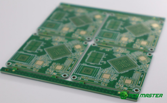
PCB shaping, also known as PCB routing or PCB cutting, is the final step in the PCB manufacturing process. Its main purpose is to separate individual PCBs from a larger panel, which contains multiple connected PCBs. This process plays a vital role in increasing production efficiency and reducing costs. By ensuring precise separation, PCB shaping ensures that each board is ready for its specific use in electronic devices.
There are two main methods of PCB shaping: mechanical processing and laser cutting. Mechanical processing typically includes methods like CNC routing and V-CUT, where a tool or blade physically cuts through the material. On the other hand, laser cutting uses high-powered lasers to vaporize material, offering more precision for intricate designs.
In the following sections, we'll dive deeper into both mechanical and laser shaping methods, explaining how to choose the best method based on the shape of your PCB, production volume, and material type. Whether you’re working with simple, rectangular designs or complex, custom shapes, understanding these methods is key to optimizing production and achieving high-quality results.
Specific Types of Mechanical PCB Shaping Methods
Mechanical shaping methods for PCBs include CNC shaping, V-CUT, stamping, and perforation, each suited to different production volumes, design complexities, and material types for efficient board separation.
CNC Shaping
How does CNC shaping work?
CNC (Computer Numerical Control) shaping uses high-speed rotating tools made from hard alloys to precisely cut PCBs. The tool follows a programmed path, allowing for intricate designs with high accuracy. CNC machines can use various tool sizes to cut different shapes, providing flexibility for various PCB requirements.
When should CNC shaping be used?
CNC shaping is ideal for medium to large production runs where high precision is required. It’s especially useful for PCBs with complex or irregular shapes, such as those with curved edges or inner cutouts. It’s also the go-to method for thick or rigid materials like metal-based or heavy copper boards.
What are the pros and cons of CNC shaping?
l Pros: CNC shaping delivers high precision and smooth edges, ensuring excellent quality and fine detail in complex designs.
l Cons: The process tends to be slower compared to other methods and can be costly due to the machinery and time involved.
V-CUT
How does V-CUT shaping work?
V-CUT shaping uses a V-shaped blade to cut a groove into both the top and bottom surfaces of the PCB. The depth of the cut is controlled, leaving a thin layer of material to hold the boards together. These boards are then separated manually or with a machine by breaking them at the weakened section.
When should V-CUT be used?
V-CUT is best suited for rectangular or regular-shaped PCBs. It works well when the connection between boards is straight, making it ideal for high-volume, standard designs where speed is key.
What are the pros and cons of V-CUT shaping?
l Pros: V-CUT is efficient for standard rectangular boards, offering high-speed production and low costs.
l Cons: It’s not suitable for irregular or curved shapes, or for boards that have components placed near the edges, as these could be damaged during the breaking process.
Stamping (Die-Cutting)
How does stamping work?
Stamping, or die-cutting, involves using a high-precision steel mold to stamp out PCB shapes from a larger panel. The die is pressed into the PCB using a stamping machine, cutting through the material in a single, high-speed action.
When should stamping be used?
Stamping is best for extremely large production runs, where the PCB shapes are simple and standardized. It's especially effective when the design is consistent and has a long lifecycle, as the cost of creating the die can be amortized over time.
What are the pros and cons of stamping?
l Pros: It’s a fast and efficient method for high-volume production, providing consistent results with minimal human error.
l Cons: The initial cost of creating the die is high, and the method is only suitable for simple designs with minimal variation. It's not ideal for low-volume production.
Perforation (Stamp Hole)
How does perforation work?
Perforation involves drilling a series of small holes along the edges of the PCB panel, making it easier to break the boards apart manually or with basic tools. This method weakens the connection between the PCBs at the drilled holes.
When should perforation be used?
Perforation is most suitable for low-volume production, particularly when the cost is a major concern. It’s commonly used for prototypes or simple designs where a manual separation of the boards is acceptable.
What are the pros and cons of perforation?
l Pros: Perforation is very cost-effective and is ideal for small batches or prototypes. It’s also simple and doesn’t require expensive machinery.
l Cons: This method is slow, prone to rough edges, and unsuitable for large-scale production due to its manual nature.
Each of these mechanical shaping methods provides specific advantages, depending on the production volume, design complexity, and material properties. Understanding which method suits your needs will help optimize both cost and quality in your PCB manufacturing process.
Specific Applications of Laser Processing Methods
Laser processing methods, particularly laser cutting, are used for high-precision, complex PCB shapes, including flexible and rigid-flex boards, as well as thin or delicate materials like ceramics and glass.
Laser Cutting for PCB Shaping
How does laser cutting work for PCB shaping?
Laser cutting uses high-powered lasers to precisely cut PCB materials. The laser beam vaporizes the material at specific points, creating clean, accurate cuts without physical contact. This method offers high precision and is particularly useful for intricate designs that would be challenging for traditional cutting methods.
When should laser cutting be used?
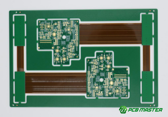
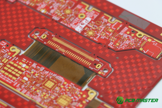
Laser cutting is ideal for producing PCBs with very small, complex shapes that require extreme precision. It's especially useful for flexible circuit boards (FPC) and rigid-flex boards, as well as materials that are thin or fragile, such as ceramic and glass-based substrates. If the PCB design involves fine details, tight tolerances, or delicate materials, laser cutting is a go-to option.
What are the pros and cons of laser cutting?
l Pros: Laser cutting provides excellent precision and eliminates mechanical stress during the cutting process, which is crucial for sensitive materials. It is perfect for designs with fine details or complex shapes that traditional methods may struggle with.
l Cons: The primary downside is the high equipment cost, making it less cost-effective for large-volume production. Additionally, the process tends to be slower compared to other methods like V-CUT or stamping.
Laser cutting is a powerful solution for high-precision, complex PCB designs, but its cost and slower speed should be considered when choosing the appropriate shaping method.
How to Choose the Right Shaping Method Based on Specific Needs?
To choose the right PCB shaping method, consider factors like the PCB shape (complex vs. standard), production volume (high vs. low), material type (hard, flexible, or standard), and any special requirements such as precision or cost sensitivity.
How to Choose the Shaping Method Based on PCB Shape?
Complex, Irregular Shapes
For PCBs with complex or irregular shapes, such as those with curves, non-rectangular outlines, or intricate cutouts, CNC milling or laser cutting is the best choice. These methods provide the flexibility needed for non-standard designs and can handle intricate patterns with high precision.
Standard Rectangular Shapes
For standard rectangular PCBs, V-CUT or stamping are commonly used. These methods are efficient for large quantities and straightforward designs, offering quick and cost-effective production for panels with a regular shape.
Curved or Special Shapes
If the PCB design includes curves or special shapes, CNC milling or laser cutting should be prioritized. These methods offer the flexibility and precision required to handle the unique contours that cannot be easily achieved with other shaping methods like V-CUT.
How to Choose the Shaping Method Based on Production Volume?
High-Volume Production
For large-scale production runs where cost efficiency and speed are critical, V-CUT or stamping are ideal choices. These methods are designed for high throughput, making them perfect for standardized designs produced in bulk.
Medium to Small Production
For medium to small batches, CNC milling is a reliable option. While slower than V-CUT or stamping, CNC milling provides the flexibility to handle a variety of designs with high precision, making it suitable for more customized or smaller production volumes.
Massive Production Volumes
For extremely high-volume production, stamping is the most efficient choice. It offers incredibly fast cutting times once the mold is created, making it the best option for manufacturers producing millions of PCBs with fixed designs.
How to Choose the Shaping Method Based on PCB Materials?
Hard Materials (e.g., Metal Substrates)
For harder materials like metal-based PCBs or thick copper boards, CNC milling or laser cutting are the best methods. These techniques provide the precision required to cut through tough, durable materials while maintaining the integrity of the board.
Flexible Materials (e.g., FPC)
For flexible circuit boards (FPC), laser cutting is the preferred method. Laser cutting allows for precise cuts without damaging the sensitive, thin layers of flexible materials. It ensures smooth edges and avoids mechanical stress, which could compromise the flexibility of the board.
Standard FR-4 Materials
For standard FR-4 PCBs, V-CUT or stamping are the most cost-effective methods. These materials are easier to cut, and V-CUT or stamping can produce high-quality results quickly and at a lower cost for standard designs.
How to Choose the Shaping Method Based on Special Requirements?
High Precision or Fine Detailing
If your design requires high precision or fine detailing, laser cutting is the best choice. Laser cutting delivers exceptional accuracy with minimal heat distortion, making it ideal for intricate patterns or tiny components on the PCB.
Smooth Edges and High Accuracy
If you require smooth edges and high accuracy, CNC milling is the go-to option. CNC milling ensures that the edges of the PCB are clean and smooth, making it perfect for high-quality, high-precision applications where edge quality is critical.
Cost-Sensitive or Low-Volume Production
For low-volume or cost-sensitive production, perforation (stamp hole) or manual cutting is a practical option. These methods are inexpensive and can be performed without high-tech equipment, making them ideal for prototyping or small batches where cost is the primary concern.
Conclusion
Choosing the right PCB shaping method involves understanding the characteristics of each available technique. CNC milling, V-CUT, stamping, and laser cutting each have their unique strengths and limitations. CNC milling is ideal for complex shapes and thicker materials, while V-CUT is perfect for standard, high-volume rectangular designs. Stamping works best for very large productions, and laser cutting is the go-to method for intricate, high-precision designs.
When making your decision, it’s important to consider four key factors: the shape of your PCB (complex or simple), the production volume (high or low), the material (hard, flexible, or standard), and any specific requirements like precision or cost. Each factor plays a critical role in determining which method will best meet your needs while maintaining cost-efficiency.
For tailored advice, consulting an experienced PCB supplier like PCBMASTER can provide you with expert guidance. As a seasoned PCB manufacturer, we can recommend the most suitable shaping methods based on your specific requirements and help optimize both production and quality for your projects.
FAQs
Why is V-CUT Not Suitable for PCBs with Components on the Edges?
V-CUT is not ideal for PCBs with components placed near the edges because the cutting process can weaken the board's structural integrity. The V-CUT method involves cutting a groove along the PCB's edges, leaving a thin layer of material to hold the panels together. If there are components on the edges, this groove could damage the components or cause them to become dislodged during the separation process. Additionally, the physical stress of separating the boards can lead to potential damage or even breakage of the PCB near these components.
What is the "Stress" Issue in PCB Shaping?
The "stress" issue in PCB shaping refers to the mechanical and thermal stresses that can be applied to the PCB during the shaping process. Mechanical stress occurs when cutting tools exert force on the material, potentially causing warping, bending, or cracking. Thermal stress, on the other hand, is generated by the heat produced during methods like laser cutting, which can cause the material to expand and contract, leading to delamination or distortion. Both types of stress can affect the functionality of the PCB and may lead to failure in the final product, especially in sensitive electronic applications.
How to Choose the Right Shaping Method for Small Batch Production?
For small batch production, flexibility and precision are key. Methods like CNC milling are well-suited for these needs as they provide high accuracy and can easily handle customized, small-volume orders. CNC milling allows for detailed designs, which is essential for prototypes or unique PCB shapes. Laser cutting is also a good choice for small batches, especially for designs requiring fine details or delicate materials. Both methods, while slower and more expensive than high-volume options, offer the flexibility needed for medium and small quantities.
Which is Better for Large-Scale Production: Stamping or Laser Cutting?
For large-scale production, stamping is the better choice. Stamping is extremely efficient when producing high volumes of PCBs with standard shapes. Once the die is created, the process is fast and cost-effective, making it ideal for mass production. On the other hand, laser cutting offers precision and flexibility, but it is slower and more expensive per unit compared to stamping. While laser cutting is great for intricate or small runs, it’s not as cost-efficient for large volumes of standardized PCBs.
Can Multiple Shaping Methods Be Combined?
Yes, combining different shaping methods is often a practical solution to meet specific production needs. For example, CNC milling can be used for the primary cutting of the PCB, while V-CUT can be used for simpler separation when needed. Combining laser cutting with CNC milling can be ideal for designs that require both high precision and the ability to cut complex shapes. This approach allows manufacturers to take advantage of the strengths of each method, optimizing both cost and quality. It’s a flexible solution that can be tailored based on design complexity and production volume.
Author Bio
Hi, I'm Carol, the Overseas Marketing Manager at PCBMASTER, where I focus on expanding international markets and researching PCB and PCBA solutions. Since 2020, I've been deeply involved in helping our company collaborate with global clients, addressing their technical and production needs in the PCB and PCBA sectors. Over these years, I've gained extensive experience and developed a deeper understanding of industry trends, challenges, and technological innovations.
Outside of work, I'm passionate about writing and enjoy sharing industry insights, market developments, and practical tips through my blog. I hope my posts can help you better understand the PCB and PCBA industries and maybe even offer some valuable takeaways. Of course, if you have any thoughts or questions, feel free to leave a comment below—I'd love to hear from you and discuss further!


