


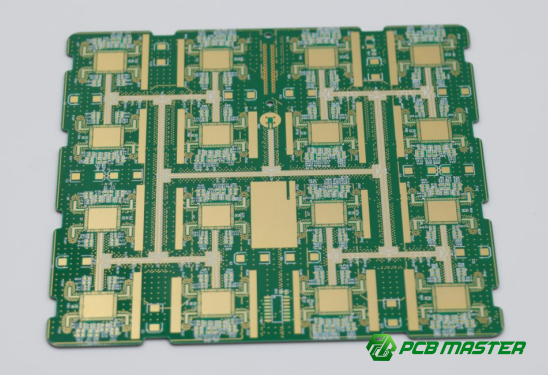
PCB Pad Design Guide: Types, Dimensions, and Best Practices for PCB Manufacturing
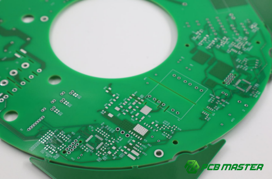
Every electronic device relies on small but critical features called PCB pads. A PCB pad is a conductive copper area on a printed circuit board where electronic components are soldered and electrically connected. Although pads occupy only a small portion of a PCB layout, they play a major role in ensuring stable electrical performance and strong mechanical connections.
Proper PCB pad design directly affects both manufacturability and assembly reliability. Pads that are too small may create weak solder joints, while oversized pads can lead to solder bridging or component misalignment. For example, an incorrectly designed pad for a surface-mount resistor can cause tombstoning during reflow soldering, reducing production yield and increasing rework costs.
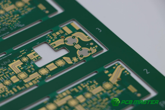
Understanding PCB pad design requires looking at several key factors, including PCB pad types, pad dimensions, and design best practices. Different applications may require through-hole pads, surface-mount pads, thermal pads, or test pads, each serving a specific purpose. Selecting the right pad size, shape, and layout helps improve solderability, manufacturing efficiency, and long-term product reliability. The following sections explain how PCB pads work, how their dimensions are determined, and which design practices help achieve consistent, high-quality PCB manufacturing results.
What Are the Main Types of PCB Pads?
The main types of PCB pads are through-hole pads, surface mount (SMD) pads, thermal pads, test pads, and custom/special-purpose pads used for different electrical, mechanical, thermal, and testing requirements in PCB design and manufacturing.
Through-Hole Pads – Structure, Function, and Applications
Through-hole pads are plated holes in a PCB that allow component leads to pass through the board and create strong electrical and mechanical connections.
Through-hole pads are made by drilling a hole in the PCB and plating it with copper. This creates a solid connection between layers and allows component leads to go through the board.
Key characteristics
· Uses drilled and copper-plated holes for connection
· Provides strong mechanical strength for heavy components
· Suitable for wave soldering or selective soldering in PCB assembly
Functions
· Provides electrical connection between PCB layers
· Offers mechanical support for high-stress components
· Improves reliability in vibration-heavy environments
Typical applications
· Power connectors and DC jacks
· Transformers and inductors
· Industrial control boards
Example: In industrial PCB manufacturing, through-hole pads are used for large electrolytic capacitors because they must stay firmly attached under vibration and high current load.
Surface Mount Pads (SMD Pads) – Structure, Function, and Applications
Surface mount pads are flat copper areas on the PCB surface used to solder components directly without drilling holes.
SMD pads are widely used in modern SMT PCB assembly and pad design. Components are placed directly on the PCB surface and soldered using reflow processes.
Key characteristics
· No drilling required, reducing manufacturing cost
· Supports very small components (e.g., 0402, 0201)
· Enables high-speed automated assembly
Functions
· Provides electrical connection for compact components
· Supports high-density PCB layout design
· Enables efficient mass production in SMT lines
Typical applications
· Smartphones and tablets
· Laptop motherboards
· IoT and wearable devices
Example: In smartphone PCB design, thousands of SMD pads are used for ICs and passive components to achieve compact and high-performance circuits.
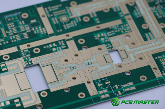
Thermal Pads – Structure, Function, and Applications
Thermal pads are large copper areas designed to transfer heat away from high-power components and improve thermal performance.
Thermal pads are used in high-power PCB design and thermal management systems. They are often placed under power ICs or MOSFETs.
Key characteristics
· Large copper area for heat spreading
· Often connected to thermal vias and inner copper layers
· Requires careful solder paste design to reduce voiding
Functions
· Transfers heat from components into the PCB structure
· Improves thermal stability of electronic circuits
· Extends component lifetime under high temperature
Typical applications
· Power ICs and voltage regulators
· MOSFET switching circuits
· LED driver and power modules
Example: In a DC-DC converter, thermal pads under the power chip help spread heat into internal copper layers, preventing overheating during continuous operation.
Test Pads – Structure, Function, and Applications
Test pads are exposed copper points used for electrical testing, debugging, and quality control during PCB manufacturing.
Test pads are designed for easy access during PCB testing and quality inspection processes.
Key characteristics
· Exposed copper surface for probe contact
· Used during testing, not final product function
· Placed on key signals like power, ground, and data lines
Functions
· Enables ICT (In-Circuit Testing) and electrical checks
· Supports debugging during product development
· Improves manufacturing yield and defect detection
Typical applications
· Production testing in PCBA factories
· Debug interfaces for engineers
· Quality inspection points in mass production
Example: In PCB assembly lines, test pads are used to quickly check whether voltage rails like 3.3V and 5V are stable before final product shipment.
Custom and Special-Purpose Pads – Structure, Function, and Applications
Custom pads are specially designed PCB pads created for unique electrical, mechanical, or high-frequency design requirements.
Custom pads are used when standard pad libraries cannot meet advanced PCB layout or signal integrity requirements.
Key characteristics
· Fully customized size, shape, and structure
· Requires close coordination with PCB manufacturers
· Needs strict DFM (Design for Manufacturability) review
Functions
· Supports RF impedance control and signal integrity optimization
· Enables mechanical integration for special connectors
· Adapts to high-speed or non-standard component designs
Typical applications
· RF antennas and communication modules
· Aerospace and automotive electronics
· High-speed digital circuit boards
Example: In RF antenna modules, custom-shaped pads are designed to control impedance and reduce signal reflection, ensuring stable high-frequency performance.
Summary Comparison
Different PCB pad types serve different roles in mechanical strength, electrical performance, thermal management, and testing functions.
| PCB Pad Type | Primary Purpose | Key Strength | Key Limitation | Typical Applications | Engineering Focus |
| Through-Hole Pads | Mechanical + electrical connection | Very high mechanical reliability | Slower manufacturing due to drilling | Power connectors, industrial boards | Structural reliability |
| Surface Mount Pads | Compact electrical mounting | High-density design and automation | Lower mechanical strength | Consumer electronics, IC boards | Miniaturization and SMT efficiency |
| Thermal Pads | Heat dissipation | Strong thermal performance | Risk of solder voiding | Power ICs, MOSFETs | Thermal management |
| Test Pads | Testing and debugging access | Easy probe access | Not part of final function | PCB testing and QA | Manufacturing efficiency |
| Custom Pads | Specialized design needs | Highly optimized performance | High design complexity | RF, aerospace, high-speed systems | Signal integrity and customization |
This classification helps engineers choose the correct PCB pad type during PCB design and manufacturing, improving yield, reliability, and production efficiency.
How Are PCB Pad Dimensions Determined?
PCB pad dimensions in PCB pad design for manufacturing (DFM) are determined by component geometry, manufacturing limits, assembly process needs, and IPC standards. The goal is to ensure good soldering, reliable electrical connection, and high production yield.
Core Pad Dimension Parameters
Core PCB pad dimension parameters define the basic size and shape of a pad, including length, width, diameter, and annular ring width.
PCB pad sizing starts with four key measurements. These parameters directly affect solder joint quality and assembly reliability in PCB land pattern design.
Pad Length
Pad length is the longer side of a rectangular pad used mainly in SMD components. It determines how much solder contact area is available along the component lead.
· Longer pad length increases solder strength
· Too long may cause solder bridging in fine-pitch ICs
· Common in SMD resistor and capacitor design
Example: In 0603 resistor pads, slightly extended pad length helps improve solder wetting during reflow soldering.
Pad Width
Pad width is the shorter side of a rectangular pad. It controls lateral solder contact and spacing between adjacent pads.
· Wider pads improve solder adhesion
· Too wide reduces spacing and increases short risk
· Critical in fine-pitch QFP and SOIC designs
Example: In QFP ICs, reducing pad width prevents solder bridging between adjacent pins.
Pad Diameter
Pad diameter applies mainly to circular pads used in through-hole designs. It defines the copper area around the drilled hole.
· Larger diameter improves mechanical strength
· Must match drill size and component lead diameter
· Important for through-hole reliability
Example: A connector pin may use a 1.6 mm pad diameter with a 0.8 mm drill hole for strong mechanical support.
Annular Ring Width
Annular ring is the copper area surrounding a drilled hole in through-hole pads. It ensures reliable electrical connection after drilling.
· Wider annular ring increases manufacturing tolerance
· Too small ring risks breakout defects
· Critical for high-reliability PCB manufacturing
Example: Industrial PCBs often require a minimum annular ring to ensure the drill does not break the copper connection.
Factors That Influence Pad Dimensions
PCB pad dimensions are influenced by component shape, manufacturing tolerances, and assembly process requirements.
Pad design is not fixed; it must be adjusted based on real-world constraints in PCB assembly and fabrication processes.
Component Package Geometry
Component package geometry defines the physical shape and pin layout of the component.
· Different packages (SMD, QFP, BGA) require different pad shapes
· Lead pitch determines spacing between pads
· Package datasheets usually define recommended land patterns
Example: A QFN package requires exposed thermal pad design, while a resistor only needs two simple rectangular pads.
Manufacturing Tolerance
Manufacturing tolerance refers to allowable variation in drilling, etching, and alignment during PCB fabrication.
· Etching can slightly reduce pad size
· Drill position may shift slightly
· Pads must be designed with safety margins
Example: PCB manufacturers often recommend adding extra margin to annular rings to avoid breakout after drilling.
Assembly Process Requirements
Assembly process requirements depend on whether SMT, wave soldering, or selective soldering is used.
· SMT requires precise pad spacing for reflow soldering
· Through-hole requires stronger mechanical clearance
· Automated assembly prefers standardized pad sizes
Example: In SMT production, tighter pad control reduces solder bridging during high-speed reflow.
IPC Guidelines for Pad Sizing
IPC guidelines provide standardized recommendations for PCB pad dimensions to ensure manufacturability and reliability.
IPC standards (such as IPC-7351) define recommended land patterns for components.
· Ensures consistent PCB pad design across manufacturers
· Improves solder joint reliability
· Reduces design errors and rework
Example: IPC guidelines define standard pad dimensions for 0603 resistors to ensure proper solder fillet formation during reflow.
Recommended Pad Dimensions for Common Packages
Recommended PCB pad sizes vary by component type to ensure proper soldering, reliability, and assembly yield.
These values are commonly used in standard PCB pad design practice, but final values depend on manufacturer rules.
0402 and 0603 Components
· Very small SMD passive components
· Require tight pad spacing and precise alignment
· Used in smartphones and compact electronics
Key point: Pads must be small enough to prevent bridging but large enough for reliable solder wetting.
SOIC Packages
· Medium-pitch IC packages
· Common in analog and power circuits
· Easier to assemble than fine-pitch ICs
Key point: Pad spacing must match lead pitch to avoid solder shorts.
QFP Packages
· Fine-pitch ICs with gull-wing leads
· Used in microcontrollers and processors
· Requires high precision PCB pad layout
Key point: Narrow pad width is critical to prevent solder bridging.
QFN Packages
· Leadless IC packages
· Require both perimeter pads and central thermal pad
· Used in high-performance compact designs
Key point: Thermal pad design is essential for heat dissipation and solder reliability.
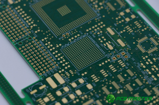
BGA Packages
· Ball Grid Array with solder balls under the chip
· Used in CPUs, GPUs, and high-speed processors
· Requires precise pad array matching
Key point: Pad size must align with solder ball diameter and reflow behavior.
Risks of Incorrect Pad Dimensions
Incorrect PCB pad dimensions can cause soldering defects, electrical failures, and reduced product reliability.
Poor pad design is one of the most common causes of PCB assembly failure in SMT and through-hole manufacturing.
· Solder bridging: Pads too close in fine-pitch ICs
· Tombstoning: Uneven pad size in small components
· Weak solder joints: Pads too small for proper wetting
· Thermal failure: Poor heat dissipation in power devices
· Assembly misalignment: Incorrect pad spacing during reflow
Example: In QFP packages, overly wide pads can cause solder to flow between pins, resulting in short circuits during SMT reflow soldering.
How Does PCB Pad Design Affect Solder Joint Reliability?
PCB pad design has a direct impact on solder joint reliability in PCB assembly, because pad geometry controls how solder spreads, bonds, and holds components over time. Poor pad design is one of the most common root causes of SMT and through-hole solder failures.
Relationship Between Pad Geometry and Solder Wetting
PCB pad geometry controls how molten solder spreads and attaches to the pad and component lead during reflow soldering.
Pad geometry (shape, size, and spacing) determines solder wetting behavior, which is how solder flows and sticks during SMT reflow soldering. Good PCB pad design for manufacturability ensures smooth and balanced wetting.
· Larger pad area improves solder spreading
· Uneven pad sizes can pull components out of position
· Correct spacing prevents solder bridging in fine-pitch designs
Example: In 0402 resistors, if one pad is larger than the other, the component may “tombstone” because solder pulls unevenly during reflow.
Effects on Joint Strength
Proper PCB pad design increases solder joint strength by maximizing contact area and ensuring balanced mechanical stress distribution.
Solder joint strength depends on how well the pad supports the solder fillet and distributes mechanical load.
· Larger pads increase bonding surface area
· Through-hole pads provide stronger mechanical anchoring than SMD pads
· Balanced pad geometry reduces stress concentration
Example: In industrial connectors, through-hole pads are used because they provide stronger pull resistance compared to surface mount pads.
Effects on Thermal Performance
PCB pad design affects how heat flows through the solder joint and into the PCB, especially in power components.
Thermal performance is critical in high-power PCB pad design, where solder joints must conduct heat away from components.
· Large copper pads help spread heat
· Thermal pads reduce hot spots under ICs
· Poor pad design traps heat, increasing failure risk
Example: In a MOSFET circuit, a well-designed thermal pad helps transfer heat into inner copper layers, preventing overheating during continuous operation.
Effects on Long-Term Reliability
Good PCB pad design improves long-term reliability by reducing mechanical fatigue, thermal stress, and solder degradation over time.
Over time, solder joints face vibration, temperature cycling, and electrical load. Pad design influences how well joints survive these stresses.
· Balanced pads reduce thermal expansion stress
· Proper copper distribution prevents cracking over time
· IPC-compliant pad design improves product lifespan
Example: Automotive PCBs use optimized pad layouts because constant vibration and temperature changes can easily crack weak solder joints.
Common Reliability Issues
Most solder joint reliability problems come from improper PCB pad size, spacing, or thermal imbalance during design.
Poor PCB pad design can directly cause assembly defects and field failures.
Insufficient Solder
Insufficient solder occurs when the pad is too small or poorly shaped, preventing enough solder from forming a strong joint.
· Weak electrical connection
· Low mechanical strength
· High risk of early failure
Example: In fine-pitch QFP ICs, small pads with poor solder paste coverage can lead to open circuits.
Excessive Solder
Excessive solder happens when pads are too large or too close, causing solder to spread too much and create bridging risks.
· Risk of short circuits
· Uncontrolled solder flow in SMT reflow
· Poor appearance and inconsistent joints
Example: In SMD resistor arrays, oversized pads can cause solder to connect adjacent pins, leading to PCB short failures.
Cracked Joints
Cracked joints occur when thermal or mechanical stress breaks the solder connection due to poor pad stress distribution.
· Caused by thermal cycling expansion mismatch
· Weak pad design increases stress concentration
· Common in automotive and industrial environments
Example: Power boards exposed to heating and cooling cycles often develop cracked solder joints if pad layout is not optimized.
Weak Mechanical Bonds
Weak mechanical bonds happen when pad design does not provide enough anchoring strength for the component.
· Components may loosen under vibration
· Common in connectors and heavy parts
· Poor through-hole or pad sizing is a key cause
Example: A poorly designed DC connector pad may loosen after repeated plugging cycles, causing intermittent connection failure.
What Are the Most Common PCB Pad Design Defects?
PCB pad design defects are manufacturing or assembly problems caused by incorrect PCB pad layout, size, spacing, or thermal structure. These defects directly affect SMT assembly yield, solder joint quality, and long-term reliability.
Tombstoning
Tombstoning is when a small component lifts on one side during reflow soldering due to uneven solder forces on PCB pads.
Tombstoning (also called “Manhattan effect”) is a common PCB pad design defect in SMT assembly, especially for small components like 0201 or 0402 resistors.
· One pad melts faster than the other during reflow
· Surface tension pulls the component upright
· Electrical connection is broken on one side
Example: In a 0402 resistor, if one pad is slightly larger or heats faster, the component stands vertically instead of lying flat, causing an open circuit.
Solder Bridging
Solder bridging happens when excess solder connects two adjacent pads, creating an unintended short circuit.
Solder bridging is a critical failure in fine-pitch PCB pad design, especially in QFP, SOIC, and high-density SMT layouts.
· Pads are too close together
· Excess solder paste spreads during reflow
· Poor solder mask design increases risk
Example: In a QFP microcontroller, incorrect pad spacing can cause solder to connect two pins, leading to IC short circuit failure.
Component Shift
Component shift is the movement of a component from its correct position due to unbalanced solder tension on PCB pads during reflow.
Component shift occurs when solder forces are not balanced between pads in PCB pad layout design.
· Unequal pad size or paste volume causes pulling force imbalance
· Component moves away from intended position
· May still be electrically connected but mechanically unstable
Example: In SMD capacitor placement, if one pad has more solder paste than the other, the capacitor shifts slightly, affecting signal stability in high-frequency circuits.
Non-Wetting
Non-wetting occurs when solder fails to properly stick to the PCB pad surface, leaving weak or open solder joints.
Non-wetting is a solder adhesion failure in PCB pad surface treatment or contamination issues.
· Poor pad surface finish (oxidation or contamination)
· Incorrect solder temperature or flux activity
· Poor PCB pad material quality
Example: A PCB stored in a humid environment may develop oxidized pads, causing solder to bead up instead of spreading evenly.
Thermal Pad Voiding
Thermal pad voiding is the formation of air gaps inside solder joints on thermal pads, reducing heat transfer efficiency.
Voiding is common in thermal pad PCB design for power components like QFN or power ICs.
· Large copper area traps air during reflow
· Poor solder paste pattern design
· Insufficient via or venting structure
Example: In a QFN power IC, large voids under the thermal pad reduce heat dissipation, causing the chip to overheat under load.
Root Causes of PCB Pad-Related Defects
Most PCB pad defects are caused by poor pad geometry, incorrect spacing, or improper thermal and solder paste design.
In PCB pad design for manufacturability (DFM), defects usually come from design-stage mistakes.
· Incorrect pad size or asymmetry
· Poor solder mask and paste mask alignment
· Insufficient thermal balance between pads
· Ignoring IPC design standards
Example: A mismatched pad pair in SMD resistors often leads to tombstoning or uneven solder joints during reflow.
Preventive Design Measures
PCB pad defects can be prevented by following IPC guidelines, balancing pad geometry, and optimizing solder paste and thermal design.
Good PCB pad design best practices significantly reduce SMT failure rates.
· Use IPC-7351 recommended pad libraries
· Keep pad pairs symmetrical for SMT components
· Optimize solder paste aperture design
· Improve thermal balance for small components
· Add proper solder mask spacing to avoid bridging
· Use DFM checks before PCB fabrication
Example: In smartphone PCB design, engineers carefully balance pad size and solder paste to prevent tombstoning in thousands of small passive components.
How Should Thermal Pads Be Designed for Effective Heat Dissipation?
Thermal pad design in PCB pad design for power electronics is focused on efficiently moving heat away from high-power components and spreading it across the PCB structure. A good thermal pad design improves device stability, reliability, and lifespan.
Purpose of Thermal Pads
Thermal pads are used to transfer heat from high-power electronic components into the PCB to prevent overheating and improve reliability.
Thermal pads are large copper areas placed under power devices such as ICs, MOSFETs, and voltage regulators. In thermal management PCB design, they act as a heat bridge between the component and the board.
· Transfer heat from chip to PCB copper layers
· Reduce junction temperature of components
· Improve long-term stability and performance
Example: In a DC-DC converter, the power IC generates heat continuously. A thermal pad helps spread this heat into inner copper layers, preventing thermal shutdown.
Thermal Pad Layout Principles
Thermal pad layout must balance heat spreading, solder support, and electrical performance to ensure stable operation.
A good thermal pad PCB layout design follows simple but critical rules:
· Use a large copper area directly under the component
· Keep thermal pad centered under the device
· Avoid sharp copper edges that block heat flow
· Ensure symmetrical design for uniform heat distribution
Example: In QFN packages, a centered thermal pad ensures even heat spreading, reducing hot spots under the chip.
Thermal Via Integration
Thermal vias are small plated holes inside thermal pads that move heat from the top layer to inner or bottom copper layers.
Thermal vias are a key part of advanced PCB thermal pad design. They improve vertical heat transfer.
· Connect top thermal pad to inner copper layers
· Increase heat dissipation efficiency
· Must be evenly distributed under the pad
Example: A power MOSFET uses multiple thermal vias under its pad to transfer heat into a large ground plane, reducing surface temperature significantly.
Solder Paste Window Design
Solder paste window design controls how solder is applied to thermal pads to ensure proper bonding and reduce defects.
In SMT thermal pad design, full solder coverage can trap air and cause issues. Therefore, paste openings are optimized.
· Use segmented or windowed paste patterns
· Avoid full solid paste coverage for large pads
· Balance solder volume to prevent overflow
Example: In QFN packages, the thermal pad is often divided into small paste windows to ensure uniform solder distribution during reflow.
Void Reduction Strategies
Void reduction strategies are methods used to minimize air pockets trapped under thermal pads during soldering.
Voids reduce heat transfer efficiency, so PCB thermal pad reliability design focuses on controlling them.
· Use via-in-pad with proper venting
· Apply step stencil printing techniques
· Optimize reflow temperature profile
· Use smaller paste apertures instead of one large area
Example: In LED driver boards, reducing voids under thermal pads improves heat transfer and prevents premature LED failure.
Example Thermal Pad Design for Power Devices
A good thermal pad design for power devices combines large copper areas, thermal vias, and optimized solder paste patterns for maximum heat dissipation.
A typical power IC thermal pad PCB design example includes:
Step 1: Copper Area Design
· Large square or rectangular copper pad under IC
· Connected to ground or thermal plane
Step 2: Thermal Via Placement
· Multiple vias evenly distributed under pad
· Connects top layer to internal copper layers
Step 3: Solder Paste Optimization
· Segmented paste pattern to reduce voids
· Balanced solder volume for stable mounting
Step 4: Heat Flow Path
· Heat moves from chip → thermal pad → vias → inner copper layers
Real example: In a laptop power management IC, this structure allows continuous operation without overheating, even under high CPU load.
What Are the Best Practices for PCB Pad Design?
Best practices for PCB pad design for manufacturability (DFM) ensure strong solder joints, high assembly yield, and long-term reliability. These rules help prevent common SMT and through-hole defects while improving production consistency.
Use IPC-Compliant Land Patterns
IPC-compliant land patterns ensure PCB pad dimensions follow standardized guidelines for reliable soldering and manufacturing consistency.
Using IPC standards (such as IPC-7351) means the pad size and shape follow proven industry rules. This reduces design errors and improves compatibility with PCB manufacturers.
· Ensures correct pad geometry for each component package
· Improves solder joint reliability and consistency
· Reduces risk of assembly defects and rework
Example: A 0603 resistor designed with IPC standard pads will solder more reliably than a custom-sized pad without standards.
Maintain Proper Solder Mask Clearance
Solder mask clearance ensures the solder mask does not cover the PCB pad and allows proper solder wetting during assembly.
Solder mask defines where solder can and cannot flow. Proper clearance prevents solder defects.
· Prevents solder mask from overlapping pads
· Improves solder wetting during reflow soldering
· Reduces risk of poor electrical contact
Example: If solder mask overlaps a QFP pad, it can block solder flow and cause weak or open connections.
Optimize Paste Mask Apertures
Paste mask apertures control how much solder paste is applied to each PCB pad during SMT printing.
Correct stencil design is critical in PCB pad assembly quality control.
· Controls solder paste volume per pad
· Prevents excessive solder or insufficient solder
· Improves balance between paired pads
Example: In 0402 components, reducing paste size slightly helps prevent tombstoning during reflow.
Ensure Consistent Pad Spacing
Consistent pad spacing ensures uniform solder behavior and prevents short circuits or component misalignment.
Pad spacing is especially important in fine-pitch and high-density designs.
· Prevents solder bridging between adjacent pads
· Ensures balanced solder tension during reflow
· Improves assembly accuracy in SMT production
Example: In QFP ICs, inconsistent spacing can easily lead to solder shorts between pins.
Consider Fabrication Tolerances
Fabrication tolerances must be considered to ensure PCB pads remain functional despite small manufacturing variations.
PCB manufacturing is not 100% perfect, so design must allow margin.
· Copper etching may slightly shrink pad size
· Drilling may shift hole position slightly
· Alignment errors must be accounted for
Example: In through-hole designs, annular ring size must be large enough to avoid breakout after drilling shifts.
Design for Automated Assembly
PCB pad design should support automated SMT and through-hole assembly to improve production speed and reduce errors.
Modern PCB production uses automated machines, so pad design must match machine requirements.
· Supports pick-and-place accuracy
· Ensures stable solder paste printing
· Reduces manual soldering requirements
Example: Symmetrical SMD pads allow robots to place components accurately without misalignment during high-speed assembly.
Balance Manufacturability and Reliability
Good PCB pad design balances easy manufacturing with strong long-term reliability in real-world operating conditions.
Designers must avoid over-optimization in one direction.
· Too small pads → weak solder joints
· Too large pads → solder bridging risks
· Balanced design improves yield and durability
Example: In automotive PCBs, pad design is slightly conservative to ensure reliability under vibration and temperature cycling.
How Can PCB Pad Designs Be Verified Before Manufacturing?
PCB pad design verification ensures that PCB pad layouts are manufacturable, reliable, and free of SMT assembly risks before fabrication. This step reduces defects, lowers cost, and improves first-pass yield in PCB production.
Design Rule Check (DRC)
Design Rule Check (DRC) is an automated check that verifies PCB pad design rules such as spacing, size, and clearance before manufacturing.
DRC is the first and most basic step in PCB pad design verification for manufacturing (DFM). It is usually performed inside PCB design software.
· Checks pad spacing and clearance between components
· Verifies minimum trace-to-pad and pad-to-pad distances
· Detects overlapping or incorrectly sized pads
Example: If two SMD pads are too close in a QFP IC layout, DRC will flag a possible short circuit risk before fabrication.
Design for Manufacturability (DFM) Review
DFM review evaluates whether PCB pad designs can be reliably manufactured using standard PCB fabrication and assembly processes.
DFM is a more advanced review compared to DRC. It is often performed by PCB manufacturers.
· Checks if pad sizes match fabrication capabilities
· Evaluates solder mask and paste mask compatibility
· Identifies risk of solder defects like bridging or tombstoning
Example: A manufacturer may adjust overly small thermal pad openings to improve solder flow and reduce voiding.
Assembly Simulation and Validation
Assembly simulation tests how PCB pads behave during soldering, placement, and reflow processes before actual production.
This step simulates SMT PCB assembly behavior to detect potential issues early.
· Simulates solder paste melting and flow
· Predicts component alignment during reflow
· Identifies imbalance in pad design
Example: In 0402 resistors, simulation may show uneven solder pull causing tombstoning risk if pad sizes are not balanced.
Prototype Evaluation
Prototype evaluation is the physical testing of a small batch PCB to verify real-world pad performance before mass production.
This step validates PCB pad design reliability under real manufacturing conditions.
· Checks solder joint quality under microscope
· Tests electrical performance of pads
· Identifies unexpected manufacturing defects
Example: A prototype run of a power PCB may reveal thermal pad voiding issues that were not visible in simulation.
Manufacturer Feedback and Optimization
Manufacturer feedback helps refine PCB pad design based on real fabrication experience and production constraints.
PCB manufacturers provide practical insights based on real production data and yield performance.
· Suggest adjustments to pad size or spacing
· Recommend solder mask or stencil improvements
· Identify high-risk assembly areas
Example: A PCB factory may recommend increasing annular ring size to prevent drill breakout in through-hole pads.
PCB Pad Design Verification Checklist
A verification checklist ensures all critical PCB pad design aspects are reviewed before manufacturing release.
This checklist is used in final PCB pad design validation for manufacturing readiness.
Dimension Review
· Checks pad length, width, and spacing accuracy
· Ensures compliance with IPC standards
· Prevents oversize or undersize pad issues
Example: Ensuring QFN pads match recommended land pattern reduces soldering defects.
Mask Review
· Verifies solder mask opening alignment
· Ensures no mask overlaps on pads
· Checks for proper solder flow clearance
Example: Incorrect mask alignment can block solder wetting on fine-pitch IC pads.
Thermal Review
· Evaluates heat dissipation paths
· Checks thermal pad and via design
· Prevents overheating in power components
Example: Poor thermal pad design in MOSFET circuits can lead to thermal failure under load.
Assembly Readiness Review
· Confirms suitability for SMT or through-hole assembly
· Checks stencil compatibility for solder paste printing
· Ensures robotic pick-and-place compatibility
Example: Symmetrical pad design ensures stable placement of small SMD components during automated assembly.
Conclusion
PCB pad design is a fundamental part of reliable PCB manufacturing because it directly affects how components are soldered, connected, and cooled. Understanding PCB pad fundamentals helps engineers build a stable foundation for both simple and complex electronic designs.
Different PCB pad types and dimension considerations, such as through-hole, SMD, thermal, and test pads, must be selected based on component structure and assembly requirements. Small changes in pad size, spacing, or shape can significantly influence production results.
More importantly, PCB pad design has a direct impact on solder joint reliability, including wetting behavior, mechanical strength, and long-term stability under heat and vibration. This is why even minor design mistakes can lead to defects like bridging, tombstoning, or weak solder joints.
To avoid these issues, defect prevention and DFM verification are essential before manufacturing. Design rule checks, manufacturer feedback, and prototype validation help ensure that PCB pad layouts are production-ready and stable in real-world conditions.
Finally, applying PCB pad design best practices—such as IPC-compliant land patterns, proper mask control, and balanced thermal design—ensures high manufacturing yield and consistent quality. For companies seeking more stable and scalable PCB and PCBA production, working with an experienced manufacturer like PCBMASTER can further reduce risks and improve overall product reliability from design to mass production.
FAQs
Can PCB pad dimensions be customized beyond IPC recommendations?
Yes, PCB pad dimensions can be customized beyond IPC recommendations, but only when there is a clear engineering reason and manufacturing validation.
IPC standards (such as IPC-7351) provide safe default land patterns, but they are not mandatory rules. Engineers sometimes adjust pad sizes for high-frequency design, space constraints, or thermal performance optimization.
However, customization must be carefully validated because:
· Smaller pads may reduce solder joint strength
· Larger pads may increase solder bridging risk
· Non-standard designs may require DFM approval from the PCB manufacturer
Example: In RF PCB design, pad shapes may be modified to control impedance, even if they differ from standard IPC footprints.
What is the minimum annular ring size for reliable manufacturing?
The minimum annular ring size is typically defined by IPC standards and must be large enough to prevent drill breakout and ensure reliable electrical connection.
In through-hole PCB pad design, the annular ring is the copper area around the drilled hole.
General industry guidance:
· Minimum annular ring is often around 0.05 mm to 0.1 mm (after drilling tolerance)
· High-reliability designs use larger rings for safety margin
· Critical for multilayer and industrial PCBs
Key risk if too small:
· Drill misalignment can break copper connection (called breakout failure)
· Reduced long-term mechanical reliability
Example: Industrial control boards use larger annular rings to ensure stable performance under vibration and thermal cycling.
Why do thermal pads require segmented solder paste openings?
Thermal pads require segmented solder paste openings to reduce voiding and improve solder reliability under large copper areas.
A full solid solder paste layer traps air during reflow, leading to thermal pad voiding, which reduces heat transfer efficiency.
Segmented openings help by:
· Allowing air and flux to escape during reflow
· Controlling solder volume more precisely
· Improving heat dissipation consistency
Example: In QFN packages, the thermal pad is divided into multiple small paste windows instead of one large block to ensure uniform solder distribution and reduce air pockets.
How do PCB pads influence SMT yield?
PCB pads directly influence SMT yield by controlling solder accuracy, component alignment, and defect rates during reflow assembly.
Poor pad design can lead to:
· Tombstoning due to unbalanced pad geometry
· Solder bridging in fine-pitch ICs
· Insufficient solder joints or weak bonding
Good pad design improves:
· Placement accuracy during pick-and-place
· Stable solder wetting during reflow
· Consistent mass production quality
Example: Balanced SMD pad sizes in 0402 resistors significantly reduce tombstoning defects in high-volume smartphone production lines.
Which PCB pad parameters are most important during DFM review?
The most important PCB pad parameters during DFM review are pad size, spacing, solder mask clearance, paste mask design, and thermal structure.
Key review points include:
· Pad dimensions: ensure compliance with component requirements and manufacturability
· Pad spacing: prevent solder bridging in fine-pitch designs
· Solder mask clearance: ensure proper solder wetting and insulation
· Paste mask aperture: control solder volume during SMT printing
· Thermal pad design: ensure heat dissipation and reduce voiding risk
Example: In a QFN IC design, DFM review often focuses on thermal pad segmentation and via placement to ensure reliable soldering and heat control.

