


PCB Layer Count Guide: How to Choose the Right PCB Layers for Your Design
Choosing the correct PCB layer count is one of the most important decisions in PCB design. The number of layers directly affects signal integrity, routing density, electromagnetic compatibility (EMC), thermal performance, manufacturing cost, and product reliability. From simple 1-layer PCBs used in LED lighting to advanced HDI multilayer boards found in automotive electronics, AI servers, and telecommunications equipment, each application requires a carefully optimized layer structure. This guide explains PCB layer counts, common layer configurations, selection criteria, and practical engineering considerations to help designers choose the right PCB layers for their projects.
What Is PCB Layer Count?
PCB layer count refers to the number of conductive copper layers contained within a printed circuit board. These copper layers are laminated together using insulating materials to form a complete PCB structure.
Each layer can perform different functions:
· Signal routing
· Power distribution
· Ground referencing
· EMI suppression
· Thermal management
As electronic products become more compact and complex, higher PCB layer counts are increasingly required to support advanced functionality and higher-speed signals.
Common PCB Layer Configurations
Different applications require different PCB layer counts.
| PCB Type | Layer Count | Typical Applications |
| Single-Sided PCB | 1 Layer | LED lighting, power supplies, calculators |
| Double-Sided PCB | 2 Layers | Consumer electronics, home appliances |
| Multilayer PCB | 4 Layers | IoT devices, industrial control systems |
| Advanced Multilayer PCB | 6–8 Layers | Automotive electronics, networking equipment |
| High-Layer PCB | 10–20+ Layers | Telecommunications, servers, aerospace |
| HDI PCB | 6–30+ Layers | Smartphones, AI hardware, wearable devices |
The optimal layer count depends on electrical requirements, design complexity, and production budget.
Why PCB Layer Count Matters
The number of PCB layers significantly impacts product performance.
Signal Integrity
Additional layers allow dedicated ground and power planes, reducing signal interference and maintaining controlled impedance.
Routing Density
Modern electronics often contain hundreds or thousands of connections that cannot fit efficiently on a simple two-layer board.
Electromagnetic Compatibility (EMC)
Proper layer stackups help reduce electromagnetic emissions and improve compliance with international standards.
Thermal Management
Multilayer boards distribute heat more effectively, improving reliability in high-power applications.
Manufacturing Cost
Higher layer counts increase fabrication complexity, but they often reduce design risks and improve long-term performance.
Understanding Different PCB Layer Structures
1-Layer PCB
A single-layer PCB contains one copper layer.
Advantages:
· Lowest manufacturing cost
· Fastest production cycle
· Simplified design process
Typical applications:
· LED modules
· Basic consumer products
· Power adapters
2-Layer PCB
Double-sided PCBs contain copper on both sides of the substrate.
Advantages:
· Increased routing flexibility
· Better component density
· Cost-effective for medium-complexity circuits
Typical applications:
· Industrial controls
· Security systems
· Consumer electronics
4-Layer PCB
A typical 4-layer stackup consists of:
1. Signal Layer
2. Ground Plane
3. Power Plane
4. Signal Layer
Advantages:
· Improved signal integrity
· Better EMI performance
· Enhanced power distribution
Typical applications:
· IoT devices
· Embedded systems
· Medical electronics
6-Layer and 8-Layer PCB
As circuit complexity increases, additional signal and reference layers become necessary.
Advantages:
· Improved routing density
· Better impedance control
· Reduced crosstalk
· Enhanced thermal performance
Typical applications:
· Automotive electronics
· Industrial automation
· Telecommunications equipment
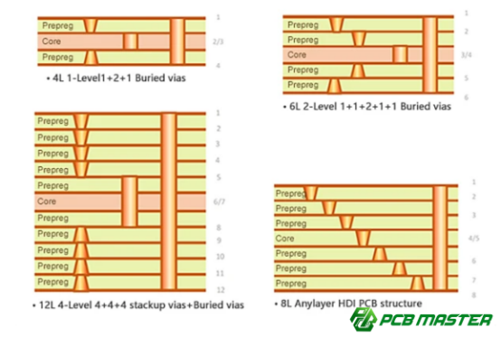
HDI PCB
High Density Interconnect (HDI) PCBs use advanced technologies such as:
· Blind vias
· Buried vias
· Microvias
· Sequential lamination
Benefits include:
· Smaller product size
· Faster signal transmission
· Higher component density
· Improved electrical performance
HDI technology is commonly used in smartphones, networking equipment, AI hardware, and advanced automotive systems.
How to Choose the Right PCB Layer Count
Selecting the right PCB layer count requires balancing performance, manufacturability, and cost.
Step 1: Evaluate Circuit Complexity
Simple circuits with limited components often require only one or two layers.
More complex products containing:
· Microprocessors
· BGAs
· FPGAs
· Dense connectors
typically require four layers or more.
Step 2: Consider Signal Speed
High-speed interfaces often require additional reference planes.
Examples include:
· PCIe
· DDR Memory
· USB 4.0
· Ethernet
· RF circuits
For these applications, 4-layer, 6-layer, or higher stackups are generally recommended.
Step 3: Assess EMI Requirements
Products requiring EMC certification benefit from dedicated ground planes and optimized stackups.
Additional layers can significantly reduce electromagnetic interference.
Step 4: Evaluate Thermal Requirements
Power electronics, industrial equipment, and automotive systems often generate substantial heat.
Multilayer boards can improve heat distribution and increase system reliability.
Step 5: Balance Cost and Performance
Choosing the lowest possible layer count may reduce fabrication costs but can increase engineering complexity and redesign risks.
A properly optimized multilayer design often reduces total project cost over the product lifecycle.
Recommended PCB Layer Count by Application
The following table provides general recommendations for common electronic products.
| Application | Recommended Layer Count |
| LED Lighting | 1 Layer |
| Power Supplies | 1–2 Layers |
| Consumer Electronics | 2–4 Layers |
| IoT Devices | 4 Layers |
| Medical Equipment | 4–6 Layers |
| Industrial Control Systems | 4–6 Layers |
| Automotive Electronics | 6–10 Layers |
| Telecommunications Equipment | 8–16 Layers |
| AI Servers | 12–30+ Layers |
| Aerospace Systems | 10–20+ Layers |
Common PCB Layer Count Mistakes
Choosing Too Few Layers
Insufficient layers can result in:
· Routing congestion
· Signal integrity issues
· Increased EMI
· Longer development cycles
Overengineering the Design
Excessive layer counts may lead to:
· Higher manufacturing costs
· Increased fabrication complexity
· Longer production lead times
Ignoring Stackup Planning
Stackup design should be considered at the beginning of PCB development rather than after routing has been completed.
Neglecting Manufacturer Feedback
Early collaboration with PCB manufacturers can prevent design issues related to:
· Via structures
· Trace width limitations
· Copper balancing
· Lamination requirements
PCBMASTER's Industry Practice and PCB Layer Solutions
As a professional PCB and PCBA manufacturer serving global industries, PCBMASTER provides comprehensive support for PCB fabrication, assembly, component sourcing, and engineering optimization.
Leveraging internationally recognized certifications including IATF 16949, ISO 9001, UL, and RoHS, PCBMASTER helps customers develop reliable PCB solutions for applications ranging from consumer electronics to automotive and industrial systems.
Core Manufacturing Capabilities
Product Type Monthly Capacity Quick-Turn PCB Prototype 1–4 Layers High Frequency PCB 50,000 pcs HDI PCB 100,000㎡ Rigid-Flex PCB 50,000㎡ FPC 6,000–10,000㎡ Metal Core PCB 20,000㎡
| Product Type | Monthly Capacity |
| Quick-Turn PCB Prototype | 1–4 Layers |
| High Frequency PCB | 50,000 pcs |
| HDI PCB | 100,000㎡ |
| Rigid-Flex PCB | 50,000㎡ |
| FPC | 6,000–10,000㎡ |
| Metal Core PCB | 20,000㎡ |
Why Engineers Choose PCBMASTER
· Free engineering file review
· 24-hour rapid prototyping
· 99.59% on-time delivery rate
· 99.5% product yield rate
· Advanced AOI inspection
· Three-stage quality control process
· Transparent pricing with no hidden costs
· One-on-one engineering support
· Self-owned 80,000㎡ manufacturing facility
Practical Example
A telecommunications customer developing a high-speed networking product initially planned a 10-layer PCB design. After PCBMASTER's engineering review and stackup optimization, the project was redesigned as an 8-layer PCB while maintaining signal integrity and EMC performance. The result was reduced manufacturing costs, simplified production, and faster product launch.
Future Trends in PCB Layer Technology
Several emerging technologies are driving demand for higher PCB layer counts:
· Artificial Intelligence infrastructure
· Automotive electronics and EV systems
· 5G and next-generation communications
· Industrial automation
· Edge computing
· Data centers and cloud infrastructure
As electronic products continue to require greater functionality within smaller footprints, multilayer and HDI PCB technologies will play an increasingly critical role in product development.
Conclusion
Selecting the correct PCB layer count is essential for achieving the right balance between performance, reliability, manufacturability, and cost. Understanding the requirements of your application—including circuit complexity, signal speed, EMC compliance, and thermal management—can help determine the most suitable PCB stackup.
By working with experienced manufacturing partners such as PCBMASTER, engineers can optimize PCB layer structures early in the design process, reduce development risks, and accelerate time-to-market while maintaining the highest quality standards.
Tags:
#PCBLayerCount #PCBLayers #PCBDesign #PCBStackup #MultilayerPCB #HDIPCB #PCBManufacturing #PCBA #SMT #PCBMASTER #ElectronicsEngineering #IndustryInsights.

