






Through-Hole PCB vs. HDI PCB: Is the Stack-Up Design Logic Fundamentally Different?
While both through-hole PCBs and HDI (High-Density Interconnect) PCBs aim to achieve signal integrity, power integrity, manufacturability, and mechanical reliability, their stack-up design logic differs significantly due to the type of vias and manufacturing processes involved .
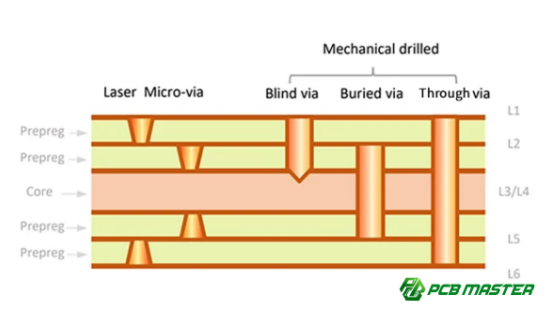
Traditional through-hole boards are built around p lated through hole s (PTH) that connect all layers in a single drilling process, making stack-up planning relatively straightforward and cost-effective. HDI boards, by contrast, rely on laser-drilled microvias, blind vias, buried vias, and sequential lamination , requiring designers to consider routing density, via hierarchy, layer build-up strategy, and manufacturing complexity from the earliest design stage.
For modern electronics utilizing fine-pitch BGAs, DDR memory, high-speed interfaces, or aggressive miniaturization targets, HDI stack-up architecture becomes a critical factor in achieving both electrical performance and physical routing feasibility.
Understanding the Fundamental Difference
The primary distinction between through-hole and HDI PCBs lies in how electrical connections are established between layers.
| Feature | Through-Hole PCB | HDI PCB |
| Via Type | Plated Through Hole (PTH) | Microvia, Blind Via, Buried Via |
| Drilling Method | Mechanical Drilling | Laser Drilling + Mechanical Drilling |
| Lamination Process | Single Lamination | Sequential Lamination |
| Routing Density | Moderate | Very High |
| PCB Size Optimization | Limited | Excellent |
| Manufacturing Complexity | Low | High |
| Cost | Lower | Higher |
| Typical Applications | Industrial Control, Consumer Electronics, Power Systems | Smartphones, Automotive Electronics, Networking, Medical Devices |
The stack-up architecture of each PCB technology evolves from these manufacturing realities.
Stack-Up Design Logic of Through-Hole PCBs
Structural Characteristics
A through-hole PCB contains vias that penetrate the entire board thickness, connecting multiple layers simultaneously.
A typical 4-layer stack-up consists of:
Top Signal LayerGround PlanePower PlaneBottom Signal Layer
Because every through-hole occupies space on all layers, routing channels become increasingly restricted as component density rises.
Design Priorities
For conventional through-hole boards, stack-up planning focuses primarily on:
- Signal integrity
- Power distribution
- EMI suppression
- Manufacturing simplicity
- Cost optimization
Typical Advantages
- Mature fabrication process
- Lower production cost
- High manufacturing yield
- Suitable for most industrial and consumer applications
- Easier engineering review and troubleshooting
For projects using component pitches larger than 0.5 mm and moderate signal speeds, through-hole stack-ups often provide the best balance between performance and cost.
Stack-Up Design Logic of HDI PCBs
Structural Characteristics
HDI technology introduces laser-drilled microvias that connect only adjacent layers.
Because microvias cannot penetrate thick laminates, HDI boards are manufactured through sequential lamination cycles , creating a layer-by-layer build-up structure.
This fundamentally changes stack-up planning.
Common HDI Structures
1-N-1 HDI
The most widely used entry-level HDI configuration.
Example:
Build-up LayerCore LayersBuild-up Layer
A 6-layer 1-N-1 design can be viewed as:
1 Build-up Layer4-Layer Through-Hole Core1 Build-up Layer
Characteristics:
- Surface microvias
- Internal mechanical vias
- Moderate cost increase
- Significant routing improvement
2-N-2 HDI
Two sequential build-up layers are added to each side.
Two common microvia approaches exist:
Staggered Microvias
- Lower manufacturing cost
- Better reliability
- Preferred for many commercial products
Stacked Microvias
- Requires copper filling and planarization
- Higher cost
- Maximizes routing density
- Common in advanced mobile devices
Any-Layer HDI
The most advanced HDI architecture.
Features:
- All interconnections achieved through laser microvias
- Maximum routing freedom
- Exceptional miniaturization capability
- Significantly higher fabrication cost
Often used in:
- Smartphones
- Wearable devices
- Aerospace systems
- Advanced automotive electronics
The Three Core Principles Behind Stack-Up Design
1. Electrical Performance
Electrical requirements drive both through-hole and HDI stack-up decisions.
Impedance Control
Controlled impedance requires careful management of:
- Dielectric thickness
- Trace width
- Copper thickness
- Material dielectric constant (Dk)
Typical impedance tolerance targets remain within ±10%.
Signal Integrity
High-speed signals should be routed:
- Adjacent to solid reference planes
- Preferably on inner layers
- With minimized return path discontinuities
HDI technology provides shorter via stubs and reduced signal reflection, making it particularly beneficial for:
- DDR memory
- PCIe
- USB4
- High-speed Ethernet
- RF applications
2. Manufacturability and Cost
Symmetrical Stack-Up
A fundamental rule applies to both technologies:
The stack-up must remain mechanically balanced.
Balance considerations include:
- Copper weight
- Dielectric thickness
- Residual copper distribution
- Layer symmetry
If one side contains significantly more copper than the other, thermal expansion mismatch can cause:
- Board warpage
- Twisting
- SMT assembly defects
- Reliability failures
This requirement becomes especially critical in automotive and mission-critical electronics.
Via Cost Impact
| Via Technology | Relative Cost |
| Standard Through Hole | Low |
| Blind Via | Medium |
| Buried Via | Medium-High |
| Staggered Microvia | High |
| Stacked Microvia | Very High |
| Any-Layer HDI | Highest |
As HDI build-up levels increase, manufacturing costs often rise exponentially.
3. Space Utilization and Layout Density
The strongest justification for HDI technology is routing density.
BGA Fan-Out Requirements
| BGA Pitch | Recommended Technology |
| ≥0.8 mm | Through-Hole PCB |
| 0.65 mm | Through-Hole or 1-N-1 HDI |
| 0.5 mm | HDI Preferred |
| ≤0.4 mm | HDI Required |
When BGA pitch reaches 0.4 mm or below, conventional through-hole routing becomes impractical.
Product Density Examples
| Product Type | Typical PCB Structure |
| Industrial Controller | 4–6 Layer Through-Hole |
| Consumer Electronics | 6–8 Layer Through-Hole / HDI |
| Automotive ADAS | 8–12 Layer HDI |
| Smartphone | 8-Layer 1-N-1 to 10-Layer 2-N-2 HDI |
Mechanical Stress Balance: The Hidden Rule of PCB Reliability
During lamination, resin flows under high temperature and pressure.
As the board cools, materials shrink at different rates, creating internal stress.
Best Practices
✔ Copper distribution should be balanced.
✔ Dielectric thickness should be symmetrical.
✔ Layer construction should mirror across the center line.
Avoid configurations such as:
- Heavy copper on one side only
- Large copper pours on one side and sparse routing on the opposite side
- Uneven dielectric build-up
Failure to maintain balance can result in:
- Board warpage
- BGA solder joint cracking
- SMT placement issues
- Reduced long-term reliability
For automotive-grade products manufactured under IATF 16949 requirements, these factors are closely monitored throughout production.
Manufacturing Limits: The Physical Reality Behind Stack-Up Design
Through-Hole Aspect Ratio
Aspect ratio is defined as:
Board Thickness ÷ Hole Diameter
A typical manufacturing limit is:
10:1
Example:
1.6 mm Board Thickness0.2 mm Drill DiameterAspect Ratio = 8:1
As aspect ratio increases:
- Drilling becomes more difficult
- Copper plating uniformity decreases
- Yield drops
Why HDI Requires Sequential Lamination
Laser-drilled microvias typically penetrate only:
70–100 μm dielectric thickness
Because microvias cannot pass through thick laminates, HDI structures must be built incrementally through multiple lamination cycles.
This physical limitation is the fundamental reason HDI stack-up strategy differs from conventional through-hole PCB design.
PCBMASTER's Engineering Perspective on Stack-Up Design
As a manufacturer specializing in PCB fabrication, PCB assembly, and SMT services, PCBMASTER supports everything from rapid-turn prototypes to advanced HDI production.
With certifications including ISO 9001, IATF 16949, UL, and RoHS , PCBMASTER applies rigorous engineering reviews before production to ensure stack-up feasibility, signal performance, and manufacturing efficiency.
Key Engineering Advantages
- Free stack-up and manufacturing review
- More than 50 professional engineers providing one-on-one support
- Advanced AOI inspection and three-stage quality control
- 99.5% product yield rate
- 99.59% on-time delivery rate
- 24-hour PCB prototype capability
- Support for HDI, Rigid-Flex, FPC, High-Frequency, and Metal-Core PCB technologies
For customers developing high-speed, space-constrained electronic products, PCBMASTER engineers frequently recommend evaluating stack-up architecture before component placement to avoid costly redesign cycles later in the project.
Conclusion
Although through-hole PCBs and HDI PCBs share common objectives such as signal integrity, reliability, and manufacturability, their stack-up design philosophies are fundamentally different .
Through-hole designs prioritize simplicity, cost efficiency, and proven manufacturability. HDI designs prioritize routing density, miniaturization, and high-speed performance through the strategic use of microvias and sequential lamination.
Choose Through-Hole PCB When:
- Cost is the primary concern
- Component pitch exceeds 0.5 mm
- Routing density is moderate
- Signal speeds are relatively low
Choose HDI PCB When:
- PCB size reduction is critical
- BGA fan-out becomes challenging
- DDR, PCIe, USB4, or RF signals require optimized routing
- Product competitiveness depends on high integration and compact form factors
As electronics continue toward higher speeds and smaller footprints, HDI technology is increasingly becoming a necessity rather than an option for next-generation product development.
Tags: #PCB #HDIPCB #PCBStackup #PCBDesign #PCBA #SMT #SignalIntegrity #HighSpeedPCB #PCBMASTER #ElectronicsManufacturing#IndustryInsights
About the Author

Carol Luo
PCB Design EngineerI'm Carol, a PCB Engineer at PCBMASTER with experience in PCB design and manufacturing engineering since 2018. I focus on translating engineering requirements into reliable PCB solutions, with expertise in stack-up design, material selection, and design-for-manufacturing (DFM). I share practical engineering insights from real-world PCB design and production experience.
Visit Carol Luo's Profile