


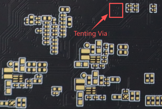
What is Tenting Via in PCB Design? A Complete Guide for Beginners
Imagine a circuit board where vias are left exposed: not only does it risk solder contamination and mechanical weakness, but it can also cause signal integrity issues. Tenting, on the other hand, helps you avoid these pitfalls, ensuring your designs are both robust and reliable. Whether you're just starting or refining your skills, mastering this simple yet essential process is key to creating PCBs that stand the test of time.
What is Tenting in PCB Design?
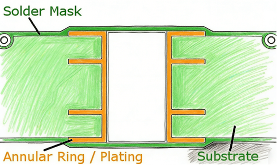
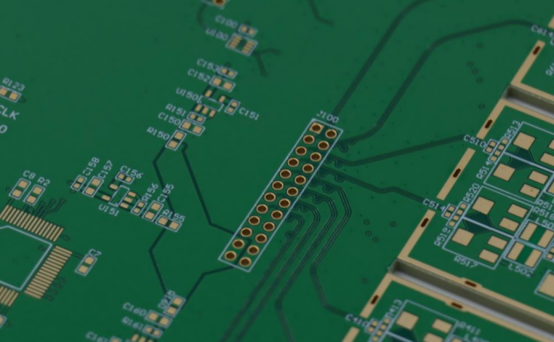
Tenting in PCB design refers to the process of covering or sealing the top of vias (small holes in the PCB that connect different layers) with a protective layer, typically a solder mask or epoxy coating. The purpose of tenting is to prevent solder, debris, or moisture from entering the via, which could lead to electrical or mechanical issues.
In a printed circuit board, vias are often drilled to allow electrical connections between different layers of the board. However, these vias, if left uncovered or exposed, can cause problems during manufacturing or use. Tenting helps address these issues by protecting the via from contaminants that could affect the performance of the PCB.
For example, if a via remains open and exposed, during soldering, excess solder could accumulate inside the via, causing a short circuit or unreliable electrical connections. Tenting prevents this by sealing the via's opening, ensuring that the board maintains its electrical integrity and physical strength.
Why is Tenting Via Important in PCB Design?
Tenting via is crucial in PCB design because it prevents a range of problems that could affect the functionality and durability of the circuit board. By covering the via openings with a protective layer, tenting ensures that no external elements, like solder, moisture, or debris, can enter the via. This simple but essential process helps to maintain the board’s electrical integrity, mechanical strength, and reliability over time.
When vias are exposed without tenting, they can attract unwanted materials that may lead to solder buildup, corrosion, or contamination. These issues can create poor connections, signal interference, and mechanical weaknesses in the board. As a result, tenting vias is a key practice to ensure that PCBs perform well and last longer, especially in sensitive applications like consumer electronics, automotive devices, or medical equipment.
What Problems Does Tenting Via Solve in PCB Manufacturing?
Preventing Solder Buildup in Vias
Exposed vias can cause solder buildup during the soldering process. When vias are not covered, excess solder may flow into the holes, causing shorts or unreliable electrical connections. By applying tenting, you can effectively seal off the vias, preventing solder from entering and ensuring clean, controlled soldering around the board.
For example, in multi-layer PCBs, which contain multiple stacked layers of circuitry, controlling solder flow into vias is essential to avoid connection errors between the layers. Tenting vias ensures that excess solder doesn’t affect the function of these layers, keeping the design intact and the connections reliable.
Avoiding Contamination in PCB Vias
Another issue addressed by tenting vias is contamination. Exposed vias are prone to collecting dirt, moisture, and flux residue during the PCB manufacturing process. This contamination can lead to corrosion and poor electrical conductivity, ultimately compromising the performance of the board.
For instance, moisture entering an exposed via could cause electrochemical corrosion over time, leading to weak or failed electrical connections. Tenting the via helps protect it from these external elements, ensuring that the PCB remains clean and functional throughout its lifecycle.
Improving Reliability and Longevity of PCBs
Tenting vias is directly tied to the reliability and longevity of a PCB. By preventing solder buildup and contamination, tenting reduces the likelihood of failures during the board’s use. For applications in high-reliability fields like medical devices or automotive electronics, where device failure can have serious consequences, ensuring the integrity of vias is critical. Tenting enhances the durability of the PCB, keeping it functioning properly for longer periods, even in harsh conditions.
How Does Tenting Affect the Electrical and Mechanical Performance?
Impact on Signal Integrity and Thermal Dissipation
Tenting vias has a positive impact on signal integrity and thermal dissipation. When vias are exposed, they can create unwanted electrical noise or capacitance that may interfere with the flow of signals, especially in high-frequency PCBs. Tenting via helps mitigate these issues by reducing the chance of signal distortion caused by debris or contaminants entering the vias.
In addition, the proper sealing of vias can help with thermal dissipation. When a via is covered and free from solder or contaminants, heat is less likely to build up in the via itself, allowing the PCB to dissipate heat more effectively. This is particularly important in high-power or high-performance PCBs, where temperature control is critical to maintaining optimal performance.
Contribution to Board Strength and Durability
Tenting vias also contributes to the mechanical strength and durability of the PCB. Exposed vias are more likely to experience wear or damage during handling or usage, especially in flexible PCBs. By sealing the vias, tenting adds an extra layer of protection, preventing mechanical failure that could compromise the entire board. This is particularly important in flexible or rigid-flex PCBs, where flexibility and durability are key design considerations.
For example, in the automotive industry, PCBs must withstand vibration, shock, and temperature fluctuations. Tenting vias helps ensure that the board maintains its mechanical integrity over time, even under challenging conditions.
How Does Tenting Via Work in PCB Design?
Tenting via works by sealing the top of vias, preventing contamination and protecting the vias from external elements that could compromise the PCB's performance. Vias are small holes drilled into the PCB that allow electrical connections between different layers of the board. When vias are left exposed, they become vulnerable to problems such as solder buildup, debris accumulation, and moisture infiltration, all of which can interfere with the board’s functionality.
Tenting involves covering the via’s opening with a thin layer of material, typically soldermask or epoxy. This prevents unwanted substances from entering the via while ensuring the surface remains clean and smooth for further assembly processes, like soldering components. Tenting improves the mechanical integrity of the PCB by preventing the vias from weakening over time due to exposure to contaminants.
For example, in high-performance devices like smartphones, where every millimeter counts and reliability is key, tenting vias ensures that the board remains free from any interference or degradation, allowing it to operate at peak performance.
What Materials are Used for Tenting Via?
Soldermask and epoxy are the most common materials used for tenting vias in PCB design. Both materials serve as effective barriers against contamination, ensuring that the vias remain clean and functional throughout the PCB’s lifecycle.
Soldermask
Soldermask is the most commonly used material for covering vias. It’s a green or other-colored polymer coating applied over the PCB surface to protect the copper traces and vias. Soldermask is known for its durability, chemical resistance, and ease of application. It effectively prevents solder from flowing into the vias during the soldering process, which could cause shorts or poor connections.
Properties of Soldermask:
Heat Resistance: Soldermask can withstand the heat used during soldering without deforming or losing its protective qualities.
Chemical Protection: It protects the vias from chemicals used in the manufacturing process, such as flux or cleaning agents.
Electrical Insulation: It provides electrical insulation, preventing shorts between the via and surrounding traces.
Epoxy
Epoxy is another material used for tenting vias, especially when a more robust seal is required. Epoxy is a strong adhesive that creates a solid, durable coating over the via. Unlike soldermask, which is applied in a thin layer, epoxy can create a thicker and more rigid seal.
Properties of Epoxy:
Stronger Seal: Epoxy provides a stronger and more durable barrier than soldermask, making it ideal for applications requiring additional mechanical strength.
Better Moisture Resistance: Epoxy provides a more waterproof seal, which is especially important in environments exposed to high moisture levels.
Electrical Insulation: Like soldermask, epoxy provides excellent electrical insulation, preventing any interference from contaminants.
In most cases, the choice between soldermask and epoxy depends on the specific requirements of the PCB, such as the need for strength, moisture resistance, or ease of manufacturing.
How is Tenting Via Applied During PCB Fabrication?
The application of tenting vias occurs during the PCB manufacturing process, typically after the vias have been drilled and plated. The process involves several critical steps, including drilling, plating, and coating. Precision at each stage is crucial to ensure the final product is of high quality and free from defects.
1. Drilling
The process starts with drilling the vias, which are small holes made in the PCB to connect different layers. Vias can be through-holes, blind vias, or buried vias, depending on the board’s design. Precision drilling is vital to ensure the vias are correctly positioned and sized.
2. Plating
After drilling, the vias are plated with a thin layer of copper. This process ensures electrical conductivity between the layers of the PCB. The plating process also prepares the vias for the next step—coating.
3. Coating (Tenting)
Once the vias are drilled and plated, the tenting process begins. The via openings are covered with soldermask or epoxy to seal them. During this step, the material is carefully applied to ensure that the vias are fully covered, without any gaps or exposed areas. This is a delicate step, as improper application could leave parts of the via unsealed, allowing contamination or solder buildup to occur.
Precision is key during the tenting step. For example, if the soldermask is applied too thickly, it may interfere with the surrounding traces and create unwanted gaps. Similarly, if the epoxy layer is too thin, it may not offer sufficient protection. The tenting process must be carefully controlled to ensure the right thickness and consistency.
Importance of Precision
Precision during the tenting step is essential to ensure that the vias are adequately sealed and the PCB performs as intended. A poorly applied tenting layer can lead to manufacturing defects, such as exposed vias or inconsistent soldering. As a result, the tenting process directly impacts the reliability and functionality of the PCB, especially in high-performance applications.
In summary, tenting vias involves applying a protective coating to vias after drilling and plating. This ensures that the vias remain free from contaminants and solder buildup, helping to maintain the PCB’s performance and longevity. Proper execution of the tenting process is crucial for high-quality PCBs, requiring careful attention to detail and precision.
Types of Tenting in PCB Design
In PCB design, tenting refers to the process of covering vias to prevent issues like contamination, solder buildup, or moisture infiltration. There are two main types of tenting methods used in PCB design: Full Tenting and Partial Tenting. Each method has its advantages, applications, and use cases depending on the design requirements.
What are the Different Types of Tenting Methods?
Full Tenting
Full tenting involves completely covering the via with a protective layer (typically soldermask or epoxy). This method seals the entire opening of the via, ensuring that no contaminants or solder can enter the hole. Full tenting is often used in situations where protection and cleanliness are essential.
Advantages of Full Tenting:
Complete protection: Prevents solder, debris, and moisture from entering the via.
Better reliability: Ensures no contamination that could lead to corrosion or signal interference.
Clean appearance: Provides a smooth, uniform surface, especially important for high-precision applications.
Use Cases for Full Tenting:
Full tenting is ideal for applications requiring high durability and cleanliness, such as medical devices, high-frequency circuits, and automotive electronics, where reliability is critical.
Partial Tenting
Partial tenting involves covering only the top of the via, leaving the rest of the hole exposed. This method is often used when the via needs to be accessible for later processes, like through-hole soldering, or when the via serves a specific purpose like thermal dissipation.
Advantages of Partial Tenting:
Cost-effective: Requires less material and time to apply, which can lower manufacturing costs.
Allows for specific functions: Leaves the via open to be used for purposes like thermal management or via-in-pad designs.
Flexibility: It provides flexibility for designs where access to the via is necessary.
Use Cases for Partial Tenting:
Partial tenting is commonly used in applications where access to the via is needed after fabrication, like in high-density interconnect (HDI) boards, or when the vias need to serve as heat sinks in power electronics.
When is Full Tenting Preferred Over Partial Tenting?
Full tenting is preferred over partial tenting in certain situations where complete protection is essential. One key example is in high-frequency circuits, where any interference, even from small contaminants in an exposed via, could affect the performance of the device. In these cases, a fully sealed via prevents signal degradation caused by debris or unwanted flux.
For example, mobile devices or high-speed communication systems rely on full tenting to avoid interference that could compromise data transmission. In these devices, vias are often used to connect multiple layers of circuitry, and even a small amount of solder buildup or contamination can create unwanted noise, leading to signal integrity problems.
When to Use Full Tenting:
High-frequency designs where signal interference must be minimized.
Critical applications such as medical, aerospace, or automotive PCBs, where failure is not an option.
Multi-layer PCBs where preventing any potential contamination inside vias is important for long-term reliability.
Pros and Cons of Each Approach
| Tenting Type | Pros | Cons |
| Full Tenting | - Provides maximum protection against contamination, moisture, and solder buildup. - Ensures stronger electrical and mechanical integrity, as the via is completely sealed off from external elements. - Creates a cleaner surface, reducing the risk of solder-related issues during assembly. | - Slightly more expensive than partial tenting due to extra material and time required. - Can limit access to vias that may be needed for post-fabrication processes (e.g., through-hole components or heat dissipation). |
| Partial Tenting | - Cost-effective, requiring less material and reducing manufacturing time. - Flexible for designs that require open vias for thermal management or component mounting. - Useful when vias are intended to serve a specific function (e.g., heat sinks or thermal vias in power supply circuits). | - Offers less protection for the via, potentially allowing contamination, solder buildup, or moisture to enter the hole. - May cause long-term reliability issues, especially in environments subject to high temperatures or moisture. |
Best Practices for Tenting Via in PCB Design
Tenting via is an essential step in ensuring the quality and reliability of a PCB. By following best practices, designers can avoid common issues and ensure that the vias are well-protected and function as intended. Let’s look at key considerations and tips for effective tenting via in PCB design.
What Are the Key Considerations for Effective Tenting Via?
Proper Via Size and Placement to Avoid Complications
The size and placement of vias are critical factors in the effectiveness of the tenting process. If vias are too small, they may be difficult to tent properly, especially in high-density designs. On the other hand, oversized vias can lead to excessive material usage, complicating the tenting process and increasing manufacturing costs.
To avoid complications, it’s important to follow the recommended via size guidelines for your PCB design. These guidelines vary depending on the PCB’s layer count and complexity. For instance, a high-density interconnect (HDI) PCB may require smaller vias to save space, but these need to be precisely placed and tented to prevent issues like contamination.
Placement is also important. Vias should be placed in areas where they won't interfere with the PCB’s functionality or structural integrity. Proper spacing between vias allows for cleaner tenting, reducing the risk of overlapping coatings or gaps in the tenting layer.
Importance of Selecting the Right Coating Material
Choosing the appropriate coating material is essential for effective tenting. Soldermask and epoxy are the most common materials, but each has its advantages and limitations.
Soldermask is ideal for standard PCB designs because it’s easy to apply and offers good protection against contamination and solder buildup. However, it may not be suitable for applications that require stronger or more durable protection.
Epoxy is more durable and offers better moisture resistance, making it the better choice for harsh environments or designs exposed to extreme conditions like high temperatures or humidity.
Selecting the right material depends on your design's environmental factors and the level of protection needed for the vias. For example, in automotive electronics, epoxy might be preferred due to its enhanced mechanical strength and resistance to temperature fluctuations.
How to Avoid Common Tenting Issues in PCB Design?
Problems like Incomplete Coverage, Exposure to External Contaminants, and Via Corrosion
One of the most common issues in tenting is incomplete coverage. This happens when the coating material does not fully cover the via, leaving parts exposed. Incomplete coverage can lead to solder contamination during the soldering process or moisture infiltration, which can cause corrosion over time.
Another issue is exposure to external contaminants. If the via is not properly sealed, debris, flux residue, or other contaminants can enter the via during manufacturing. This can result in poor electrical performance, leading to failures or unreliable connections.
Via corrosion is another significant problem, especially in high-humidity environments. When vias are exposed, moisture can enter and react with the copper inside the via, causing oxidation and weakening the connection between layers.
How to Resolve These Issues During the Design Phase
To resolve these issues during the design phase, ensure that the following best practices are followed:
Ensure Complete Coverage: When designing the PCB, use simulation software to check for any gaps in the tenting material. Conduct a DFM (Design for Manufacturability) check to ensure that the vias are properly tented without any incomplete areas.
Proper Cleaning and Preparation: Before applying the tenting material, ensure that the PCB is thoroughly cleaned to remove any flux, oils, or contaminants that could interfere with the coating's adhesion.
Select Appropriate Coating Material: Choose the correct coating material based on the application needs. If your design will be exposed to high humidity or extreme temperatures, opt for epoxy instead of soldermask for better protection. Ensure that the coating is applied evenly, covering the entire via without leaving gaps.
Use the Right Via Placement and Size: Avoid placing vias too close together or in locations where tenting may be compromised. Larger vias should be used with caution, as they may require additional material for proper coverage.
By addressing these issues during the design and fabrication phases, designers can ensure that the vias are properly protected, reducing the risk of electrical failures and improving the overall reliability of the PCB.
How Does Tenting Via Impact the Cost of PCB Manufacturing?
Tenting via adds an extra layer of complexity to the PCB manufacturing process, which can impact overall costs. However, the increased expense often brings significant benefits in terms of reliability, performance, and longevity of the PCB. Understanding how tenting affects cost is essential for designers to make informed decisions about when and where to apply it.
Does Tenting Via Increase the Manufacturing Cost?
Cost Comparison Between Tented and Non-Tented Vias
Yes, tenting vias does increase the manufacturing cost compared to non-tented vias. This cost increase primarily comes from the additional materials and labor involved in applying the tenting layer. The process requires a coating (typically soldermask or epoxy) to cover the vias, which requires both time and resources to apply properly.
Non-tented vias, on the other hand, do not require this extra step, resulting in lower material usage and less labor. While non-tented vias are simpler to manufacture, they leave vias exposed, potentially leading to issues like solder contamination, signal interference, or moisture infiltration, which could result in long-term reliability issues or failures.
For example, in low-cost consumer electronics where board performance is less critical, manufacturers may choose non-tented vias to save on production costs. However, in high-performance applications such as medical devices or aerospace electronics, the cost of tenting vias is considered a necessary investment for ensuring the board’s reliability and function.
Influence on Time, Material Usage, and Labor
The application of tenting vias increases both production time and material usage. Tenting requires additional steps, including coating the vias, curing the coating, and performing quality checks to ensure proper coverage. This can add to the manufacturing timeline, especially if there are issues with applying an even coat or if the vias are located in hard-to-reach areas of the board.
The materials used in tenting, such as soldermask and epoxy, also add to the overall cost. Soldermask is relatively inexpensive, but the extra layers of epoxy or other more specialized materials can increase costs further, especially in cases where high durability or moisture resistance is needed.
How to Balance Cost and Functionality in Tenting Via?
When to Invest in Tenting for Functionality vs. Cost-Saving Measures
When deciding whether to invest in tenting vias, it's important to consider the functionality of the board and its intended use. For low-cost consumer products, where performance and durability are less critical, cost-saving measures like non-tented vias may be appropriate. This allows manufacturers to keep the price of the board low while still meeting the basic requirements.
However, for applications that demand high reliability and long-term durability, such as medical devices, automotive electronics, or aerospace systems, the investment in tenting is crucial. In these cases, the cost of tenting is justified by the need to protect the vias from contaminants and ensure the PCB’s longevity under harsh conditions.
Strategies for Optimizing the Cost-Effectiveness of Tenting
1. Selective Tenting
One cost-saving strategy is selective tenting, where only certain vias that are critical to the board’s performance are tented, while others are left exposed. This can help reduce the overall material and labor costs while still providing adequate protection where necessary.
For instance, in high-speed signal processing circuits, tenting vias connected to the signal layer can ensure optimal signal integrity, while vias in non-critical areas may remain untented to reduce costs.
2. Use of High-Quality Soldermask
Opt for high-quality soldermask materials that provide excellent protection at a lower cost compared to epoxy. High-quality soldermask can offer better moisture resistance and solder protection without the need for more expensive epoxy layers.
3. Automated Tenting Application
Using automated machines for the tenting process can also reduce costs by increasing the speed and precision of application. Automation helps to ensure consistent, high-quality coverage without requiring excessive manual labor, which can drive up costs.
4. Design Optimization
Optimizing the via design (size, placement, and quantity) can also reduce the need for excessive tenting. By strategically placing vias and choosing appropriate sizes, designers can minimize the number of vias that need to be tented, thus saving on material and labor costs.
Real-World Applications of Tenting Via in PCB Design
Tenting vias are critical in various industries where PCB reliability, durability, and performance are paramount. By covering the vias to prevent contamination, moisture, or solder buildup, tenting ensures the PCB maintains its integrity throughout its lifecycle. Let’s explore which industries benefit most from this process and how different types of PCBs require customized tenting approaches.
What Industries Benefit Most from Tenting in PCB Design?
Consumer Electronics
In the world of consumer electronics, such as smartphones, laptops, and wearable devices, tenting vias is crucial for ensuring long-lasting performance. These devices undergo frequent handling, exposure to moisture, and varying temperatures. Tenting helps prevent corrosion, contamination, and solder buildup, all of which could lead to failures or performance degradation over time. For instance, smartphones often have multi-layered PCBs with vias that must be fully sealed to prevent failure in high-stress environments.
Automotive
The automotive industry requires PCBs that can withstand high temperatures and vibration while remaining reliable for years. Tenting vias in automotive PCBs helps protect them from dust, moisture, and other contaminants that could interfere with the board’s functionality. In electric vehicles (EVs) and autonomous driving systems, where PCBs control critical systems like sensors, power management, and communication, tenting is a necessary step to prevent signal interference and ensure longevity.
Medical Devices
In medical devices, PCBs are often required to function reliably under extreme conditions, such as high humidity or prolonged exposure to liquids. Tenting vias prevents contamination and corrosion, ensuring that the medical equipment, like heart monitors or implantable devices, operates safely and without malfunctions. Given the critical nature of these devices, tenting is essential to protect the vias from causing electrical failures that could jeopardize patient safety.
Telecommunications
Telecommunications equipment, such as base stations and network routers, relies on highly reliable PCBs to transmit data without disruption. Tenting vias is vital for minimizing the risks of contamination or solder buildup, which could impact signal integrity or cause intermittent connection issues. For 5G infrastructure, where performance is crucial, the quality of the PCB’s vias—protected by tenting—ensures seamless connectivity and minimal downtime.
How Do Different PCB Types Require Different Tenting Approaches?
Rigid PCBs
Rigid PCBs are the most common type of PCB, found in products ranging from consumer electronics to automotive components. Tenting via on rigid boards is straightforward because the board itself does not bend or flex. The primary concern is ensuring the vias are well-protected from contaminants and solder buildup, which could lead to electrical shorts or poor performance. For most rigid PCBs, soldermask is used to cover the vias, providing sufficient protection in standard applications like smartphones or TV circuits.
Example: In home appliances like washing machines or refrigerators, rigid PCBs are used to control motors and sensors. Tenting the vias ensures that these devices continue working reliably, even in humid environments.
Flexible PCBs
Flexible PCBs are used in applications where the board needs to bend or conform to specific shapes, such as in wearable devices or foldable smartphones. Tenting vias on flexible boards requires special attention because the flexibility of the board can affect the coating's adhesion. Epoxy or polyimide coatings may be used for flexible PCBs to ensure that the tenting layer stays intact even under repeated bending or flexing. Tenting on flexible PCBs also prevents moisture and contamination from seeping into the vias, which could affect the electrical connections between layers.
Example: A fitness tracker uses a flexible PCB that bends around the wrist. Tenting the vias ensures the board remains durable, maintaining its performance even after extended use.
Rigid-Flex PCBs
Rigid-flex PCBs combine the advantages of both rigid and flexible boards, allowing them to bend in some areas while staying rigid in others. These PCBs are often used in applications like medical devices and aerospace systems, where both flexibility and durability are crucial. Tenting vias on rigid-flex PCBs requires careful planning, as the coating needs to accommodate both the rigid and flexible parts of the board. Selective tenting may be used, where only the vias in the rigid areas are fully covered, while the flexible parts are treated differently.
Example: In an aerospace system with a rigid-flex PCB, tenting is applied to the rigid sections that are exposed to harsh conditions, while flexible areas may have different treatment to allow for movement without compromising the vias’ protection.
Troubleshooting Tenting Via Problems in PCB Design
Tenting vias is an essential part of ensuring that a PCB performs reliably over time. However, problems can occur during the design or manufacturing process, which may affect the effectiveness of the tenting and the overall quality of the PCB. By understanding common tenting issues and how to test for them, you can ensure that your PCB functions as intended.
What Are Common Tenting Via Issues and How to Fix Them?
1. Misalignment of Tenting Layer
Problem:
Misalignment occurs when the tenting layer (usually soldermask or epoxy) does not perfectly cover the via hole. This can happen if the via is poorly positioned or if there’s a mistake during the photolithography process used to apply the tenting material. Misalignment leaves portions of the via exposed, leading to potential contamination or solder buildup.
Solution:
To fix this, you need to verify the via positioning during the design phase using software like DFM (Design for Manufacturability) tools. Ensure that vias are placed with sufficient spacing and that the tenting layer is correctly aligned. During manufacturing, accurate mask alignment and high-quality photolithography will help reduce misalignment.
Real-World Example:
A smartphone PCB with poorly aligned vias could lead to soldering issues, with excess solder spilling into the vias, potentially causing electrical shorts. This is avoided by ensuring tight alignment control during the design and fabrication process.
2. Incomplete Tenting Coverage
Problem:
Incomplete tenting coverage happens when the tenting layer doesn’t fully cover the entire via, leaving small gaps or portions of the via exposed. This issue is often caused by an insufficient coating thickness or defective application of the tenting material, which can lead to moisture ingress, contamination, or solder buildup inside the via.
Solution:
Ensure that DFM checks are carried out to validate the tenting coverage during the design phase. During manufacturing, consistent coating thickness and proper curing of the tenting material are essential. Additionally, regular quality checks like automated optical inspection (AOI) during production can help identify areas where coverage may be incomplete.
Real-World Example:
In medical devices where PCB reliability is critical, incomplete tenting could result in circuit failure due to contamination. To avoid this, manufacturers use soldermask with precise application methods to ensure full coverage.
3. Overlapping Tenting Layers
Problem:
Overlapping tenting layers occur when the coating material extends beyond the via’s opening and onto surrounding traces or pads. This could affect soldering and may cause short circuits or poor electrical connections during the PCB assembly process.
Solution:
Carefully control the application of the tenting material, making sure it’s applied only to the via opening and not over the surrounding areas. Automated dispensing systems and screen printing can help control material application and avoid overlaps.
Real-World Example:
In high-frequency RF PCBs, overlapping tenting layers could cause signal degradation. To prevent this, precision coating techniques are used to ensure tenting material only covers the via and not the surrounding pads.
How to Test Tented Vias for Quality Assurance?
1. X-Ray Analysis
What It Is:
X-ray inspection is a non-destructive testing method used to look inside the PCB and examine whether the tenting layer covers the vias correctly. X-ray technology can reveal if there are any gaps, voids, or solder buildup inside the via that isn’t visible on the surface.
How It Helps:
X-ray analysis is particularly useful for detecting issues with hidden vias or those inside multi-layer PCBs, where traditional visual inspection won’t suffice. It allows for a thorough check of via coverage without damaging the board.
Example:
For a medical implantable device PCB, using X-ray analysis ensures that all vias are properly sealed, preventing contamination and ensuring the device functions safely inside the human body.
2. Optical Inspection (AOI)
What It Is:
Automated Optical Inspection (AOI) uses high-resolution cameras and software to scan the PCB surface for defects. This method visually inspects the tenting layer to check for alignment issues, incomplete coverage, or unwanted overlaps.
How It Helps:
AOI is quick and effective at detecting surface issues like misalignment, incomplete coverage, and overlapping layers. It’s often used during the production process to catch problems early before moving forward with assembly.
Example:
In consumer electronics, such as laptops, AOI can be used to inspect each board during the manufacturing process. Any vias with poor tenting coverage are flagged, preventing defective boards from reaching assembly.
3. Electrical Testing (ICT and Flying Probe Testing)
What It Is:
In-circuit testing (ICT) and flying probe testing are methods used to test the electrical performance of the PCB by checking for shorts or open circuits. These tests help detect any issues that might arise from improperly tented vias, such as poor connections or unintended shorts.
How It Helps:
By checking the electrical integrity of vias and traces, these tests can confirm whether the tenting process has successfully protected the vias from contamination or interference. If any issues are detected, corrective actions can be taken before the board is sent for final assembly.
Example:
In automotive PCBs, where electrical reliability is essential for safety systems like airbag sensors or anti-lock braking systems, ICT and flying probe testing help ensure all vias are properly sealed and conductive.
Conclusion: The Role of Tenting Via in PCB Design
Tenting vias is essential for ensuring PCB durability and performance. It protects vias from contamination, moisture, and solder buildup, preventing electrical failures and corrosion. Whether in consumer electronics or critical applications like medical devices, tenting improves the reliability of multi-layer PCBs.
By using the right materials and precise techniques, designers can optimize PCB quality and longevity. PCBMASTER, a trusted PCB supplier, specializes in high-quality PCBs with advanced processes like tenting via. We deliver reliable and durable boards tailored to your needs. Contact us for your next PCB project and experience top-tier manufacturing.
FAQs
Why is Tenting Via Necessary for PCB Design?
Tenting via is crucial for PCB design as it offers several functional benefits that improve the overall reliability of the board. One of the primary advantages is preventing solder contamination. Without tenting, solder can enter the via during the soldering process, leading to short circuits or poor electrical connections. Tenting the via with a protective coating like soldermask ensures that the via remains clean and free from contaminants.
Tenting also improves mechanical integrity. Exposed vias can weaken the structure of the PCB, making it more prone to damage from stress, vibration, or handling. By sealing the via, tenting ensures the PCB retains its strength and durability, especially in high-reliability applications like automotive, medical devices, or aerospace.
Can Tenting Via Impact PCB Signal Integrity?
Yes, tenting vias can influence PCB signal integrity, but it depends on the materials used and the application process. In general, soldermask is often used for tenting, and it can help improve signal integrity by preventing contamination that might affect the quality of the signals transmitted through the board.
However, if the tenting process is not executed correctly—such as when the material is improperly applied or too thick—it can cause issues. For example, excessive tenting material could lead to signal distortion or impedance mismatch, particularly in high-frequency applications like RF circuits. Therefore, it's essential to ensure that tenting is applied precisely to prevent any negative impact on the board’s performance.
Is Tenting Via Expensive to Implement in PCB Manufacturing?
Tenting vias does add to the cost of PCB manufacturing, but the increase is typically minimal compared to the benefits it offers in reliability and durability. The primary cost factors include the materials (like soldermask or epoxy), the extra manufacturing steps required to apply and cure the coating, and the labor involved in ensuring the tenting process is properly executed.
For instance, using epoxy or specialized coatings for higher protection in demanding environments like automotive or medical devices can raise costs slightly. However, this cost is often justified by the reliability and long-term performance improvements, which are critical for safety and functionality in high-stakes industries. In general, tenting vias are a cost-effective investment for mission-critical applications where long-term board performance is essential.
What Happens If Tenting Via Is Not Applied in PCB Design?
If tenting is not applied to vias in PCB design, several potential issues can arise:
Contamination: Exposed vias are susceptible to moisture, dust, and chemical contamination, which can result in corrosion and electrical shorts. Contaminants can enter the via and interfere with the electrical paths inside the PCB, causing long-term reliability issues.
Soldering Problems: Without tenting, solder can seep into the via during assembly, creating unwanted bridges or unpredictable solder joints, which could affect the PCB’s signal integrity and mechanical reliability.
Mechanical Weaknesses: Unsealed vias make the board structurally weaker. When vias are exposed, they can cause stress points on the PCB, increasing the risk of cracks, especially under thermal expansion or physical pressure. This is a serious concern in high-performance or mobile devices.
Thus, the absence of tenting can compromise the functionality and long-term durability of the PCB, making it vulnerable to failures.
Can Tenting Via Be Applied to All Types of Vias?
Tenting via can be applied to most types of vias, but the process varies depending on the via type. Common vias include through-hole vias, blind vias, and buried vias.
Through-Hole Vias: These are the most common and are typically suited for tenting. Since they extend all the way through the PCB, applying tenting helps prevent contamination on both sides of the board, which is particularly important in multi-layer PCBs.
Blind Vias: Blind vias connect an outer layer to one or more inner layers but do not go all the way through the board. Tenting is often applied to blind vias to prevent contamination or solder buildup from the outer layers.
Buried Vias: Buried vias connect the inner layers of the PCB and are typically not exposed to the external environment. While tenting is not required for most buried vias, some designs may still apply tenting to prevent issues like moisture ingress from internal layers, especially if the vias are near components susceptible to environmental damage.
In summary, tenting can be applied to most via types, but its necessity and approach depend on the specific via type and the design’s requirements.
Author Bio
Hi, I'm Carol, the Overseas Marketing Manager at PCBMASTER, where I focus on expanding international markets and researching PCB and PCBA solutions. Since 2020, I've been deeply involved in helping our company collaborate with global clients, addressing their technical and production needs in the PCB and PCBA sectors. Over these years, I've gained extensive experience and developed a deeper understanding of industry trends, challenges, and technological innovations.
Outside of work, I'm passionate about writing and enjoy sharing industry insights, market developments, and practical tips through my blog. I hope my posts can help you better understand the PCB and PCBA industries and maybe even offer some valuable takeaways. Of course, if you have any thoughts or questions, feel free to leave a comment below—I'd love to hear from you and discuss further!

