


What is Step Trenches in PCB? Uses, Manufacturing Process & Benefits Explained
PCB manufacturing has always been about pushing the limits of space and efficiency. As technology demands smaller, faster, and more powerful devices, designers face growing challenges in fitting high-density components onto ever-thinner boards. This is where the concept of step trenches, or controlled-depth slots, comes in—an advanced technique that allows manufacturers to create precise recesses within the layers of a PCB without cutting through the entire board. By carefully controlling the depth, step trenches offer unique solutions to problems like reducing assembly height, enhancing heat dissipation, and even improving signal integrity. Yet, while they open up new possibilities, these slots also come with their own set of challenges. Understanding the intricacies of step trench design and manufacturing can make all the difference in creating cutting-edge, high-performance PCBs for industries like consumer electronics, aerospace, and communications.
What are Step Trenches?
Step trenches are a type of controlled-depth slot created within a PCB, where material is removed layer by layer without piercing through the entire board. These trenches are commonly used to solve complex design challenges, such as reducing height in multi-layer boards or improving signal integrity. They allow for precise manipulation of the board's structure, enabling manufacturers to design compact, high-performance electronics.
Understanding Step Trenches
What is a Step Trench?
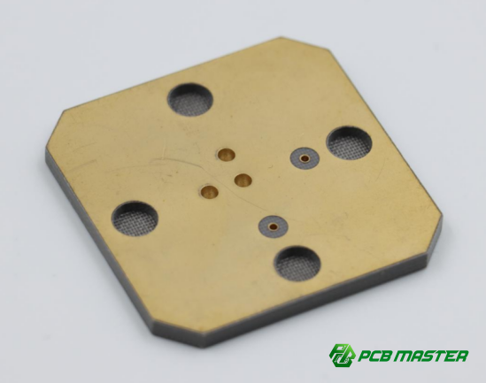
A step trench, also known as a controlled-depth slot, is an indentation made in specific layers of a PCB. Unlike regular through-holes or V-CUTs, which cut all the way through the board, a step trench only removes material from certain layers. This results in a "stepped" profile, similar to a multi-floor building, where each layer is processed independently. The depth of the trench is precisely controlled to avoid damaging other layers.
Key Concept – "Floors" in Step Trenches:
The "floors" in step trenches refer to the specific layers within a multi-layer PCB where material is removed. Think of it as cutting into the middle of a layered cake, but only scooping out a portion of one layer without disturbing the other layers. The depth of the trench is adjusted to precisely match the needs of the design, often to accommodate components, improve heat dissipation, or facilitate signal routing.
Step Trenches vs. Standard V-CUTs or Through-Holes
| Feature | Step Trench | V-CUT (Stamp Hole) | Through-Hole |
| Penetration | Does not go through the entire PCB | Typically cuts through the entire board | Fully penetrates through the board |
| Control Depth | Depth is controlled and specific to layers | Depth is uniform throughout the board | Depth is fixed based on drill size |
| Usage | Used for space-saving and high-density designs | Common in multi-board connections | For component mounting or electrical connection |
| Advantages | Allows more precision and flexibility in design | Simple and low-cost manufacturing | Strong, reliable connection |
Step trenches provide more precise control over which layers are affected, unlike V-CUTs, which are often used to create separations or connections through the entire board. This control is key for complex designs requiring different depths and features.
Key Features of Step Trenches
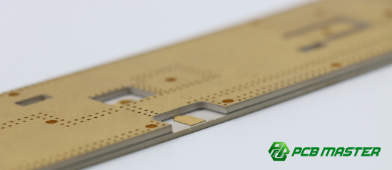
1. Non-Penetrative Design:
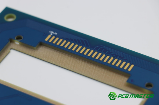
One of the defining features of a step trench is that it is non-penetrative. This means that the slot does not cut through the full thickness of the PCB, preserving the integrity of the other layers. This is a major advantage when working with complex multi-layer boards where only specific layers need adjustments. For example, in high-density interconnect (HDI) boards used in smartphones, the trenches are often used to create space for components like chips or connectors without compromising the surrounding layers.
2. Controlled Depth:
Step trenches offer high precision in depth control, ensuring that the material removal is limited to only the necessary layers. For example, if a trench is needed only to accommodate a component on the second layer of a PCB, the depth can be precisely controlled to match that requirement, without affecting the other layers above or below. This level of control is critical for applications where signal integrity or thermal management is important, such as in high-speed digital circuits or power electronics.
3. Wall Metallization (or Non-Metallization):
The sidewalls of step trenches can either be left non-metalized or metallized with copper. Metallization is often used to provide electrical continuity between different layers of the PCB, especially in cases where the step trench serves as a pathway for signals or power. On the other hand, non-metalized sidewalls are often used to create physical separations or reduce interference between components.
4. Manufacturing Complexity:
While the precision and customization offered by step trenches provide significant advantages, the process is more complex compared to regular drilling or V-CUT techniques. The controlled depth, sidewall treatment, and need for high precision require advanced machinery and careful process monitoring. This makes manufacturing step trenches more expensive and technically demanding. For instance, precision-controlled milling machines or laser cutters are typically required to achieve the exact depth and finish.
What Are the Classifications and Standards for Step Trenches?
Step trenches are classified based on their design characteristics, especially the level of metallization and the depth of the slot. There are three primary classifications that differentiate how these trenches are created and their applications in PCB manufacturing. Additionally, specific industry standards, such as IPC-6012F, help ensure that the step trenches meet the necessary quality requirements for functionality and reliability.
What Are the Classifications of Step Trenches?
Step trenches are divided into three types, based on the level of metallization on their sidewalls and bottoms. These classifications are important because they influence both the manufacturing process and the application of the step trench.
Type 1 Step Trenches
Type 1 step trenches have no metallization on the bottom or sidewalls of the trench. This means the trench is purely a physical indentation, typically used when no electrical connection is required between the PCB layers. These are often used for space-saving purposes or to make room for components that do not require electrical contact. For instance, in a wearable device, a Type 1 step trench could be used to reduce the height of a component without affecting the overall functionality of the PCB.
Type 2 Step Trenches
Type 2 step trenches feature metallization on the bottom of the trench, but not on the sidewalls. The metallization allows for electrical continuity between different PCB layers through the trench's bottom, making it suitable for connecting power or ground layers. However, the absence of sidewall metallization limits its use for more complex signal paths. This type is often used in medium-density applications like certain communications equipment, where you need some electrical connections but don’t need full sidewall conductivity.
Type 3 Step Trenches
Type 3 step trenches have metallization on both the bottom and the sidewalls of the trench. This is the most advanced type, offering complete electrical continuity through the trench from layer to layer. Type 3 trenches are typically used in high-speed or high-frequency PCBs where a continuous electrical path is necessary between multiple layers of the PCB. This type is common in high-performance electronics such as RF devices and high-frequency circuit boards, where electrical signal integrity is critical.
What Are the IPC-6012F Inspection Standards for Step Trenches?
The IPC-6012F standard provides specific inspection and quality requirements for step trenches to ensure they meet the necessary design and performance criteria. These standards focus on several key factors, including size, surface coating, and the quality of the metallization process.
Size Requirements
The size of the step trench—its length, width, and depth—must adhere to strict design specifications outlined in the IPC-6012F standards. These dimensions must be accurate to ensure proper functionality and to avoid any interference with other layers or components on the PCB. For example, the trench depth must be controlled precisely to ensure that the PCB's integrity is maintained without damaging other layers or components. Failure to meet the size specifications can result in structural weaknesses or electrical problems.
Surface Coating and Void Limits
The standard also specifies how the surface coating on the step trench should be applied, particularly regarding the presence of voids or gaps in the coating. Voids on the sidewalls of the trench, particularly in Type 2 and Type 3 trenches, can create weak points or gaps in electrical continuity. For example, in Type 2 trenches, the void size should not exceed a certain percentage of the sidewall area. Similarly, the coating on the bottom of the trench in Type 3 must be smooth and free of defects to ensure reliable electrical conductivity. The specific limits for voids are defined in the IPC-6012F guidelines to maintain the performance and reliability of the PCB.
Exposed Fiber and Plating Requirements
The IPC-6012F standard also defines the tolerance for exposed fiber and the quality of the plating used in the step trench. Exposed fiber refers to instances where the base material of the PCB is visible in the trench, which can happen if the plating process is incomplete. This could lead to issues like signal interference or weak spots in the trench. The standard specifies that exposed fiber should be minimal, and if present, it should not interfere with the trench’s functionality. Additionally, the plating (copper or other metals) must meet strict thickness and uniformity requirements to ensure the trench performs as intended without introducing defects.
What Are the Main Applications of Step Trenches?
Step trenches in PCB manufacturing are used to solve various design challenges. From saving space and improving component integration to optimizing heat dissipation and shielding, step trenches provide flexibility and precision. Below are some of the primary applications of step trenches in modern PCB design.
How Are Step Trenches Used in Component Embedding?
Step trenches allow for the embedding of components within a PCB, reducing overall assembly height and creating a more compact design.
Reducing Assembly Height:
Step trenches enable the placement of components below the surface of the PCB, effectively lowering the overall height of the assembly. This is particularly useful in products where space is limited, such as smartphones, wearables, and IoT devices. By carving out a trench in the PCB, components like chips, capacitors, or connectors can be "buried" within the board, leaving the surface level for other components.
Applicable Products:
This technique is commonly applied in high-density electronic devices where maintaining a slim profile is essential. For example, in mobile phones, the use of step trenches allows for better utilization of limited space while maintaining functionality, ensuring the design is both compact and efficient.
What Are the Advantages of Step Trenches in Connector/Module Installation?
Step trenches provide a unique solution for integrating connectors or modules in PCBs, offering advantages in terms of mechanical stability and compact design.
Connector Insertion Advantage:
By using a step trench, connectors or modules can be inserted directly into the PCB, reducing the need for bulky, external connectors. This is especially useful for applications that require a more permanent, stable connection between boards, like in multi-board systems or when connecting a PCB to a flexible circuit (FPC).
Sturdier, More Compact Design:
Inserting connectors into the step trench enhances the mechanical stability of the PCB, as it provides a more secure fit compared to traditional surface-mount connectors. This method also saves space, allowing for more compact designs without sacrificing functionality. For instance, high-density connectors used in medical devices or wearables benefit from this approach, as it ensures durability while reducing the overall footprint.
How Do Step Trenches Help with Heat Dissipation?
Efficient heat dissipation is critical for high-power components. Step trenches can improve thermal management by providing more direct contact with heat sinks or heat dissipation materials.
Optimizing Heat Pathways:
Step trenches can be used to create a direct path for heat to flow from the component to the PCB surface, which can then be connected to a heat sink or other thermal dissipation solutions. The trench allows for better placement of thermal pads or conductive materials that can effectively transfer heat away from sensitive components.
High-Power Components:
This technique is especially useful for high-power components, such as power transistors or processors, which generate a lot of heat during operation. In products like gaming computers or power supply units, step trenches provide a way to manage thermal load more efficiently, preventing overheating and ensuring the longevity of the device.
How Do Step Trenches Improve Electromagnetic Shielding?
Step trenches play a role in enhancing electromagnetic compatibility (EMC) by improving shielding effectiveness and reducing interference.
Improving Shielding Performance:
Step trenches can be used to create a path for electromagnetic shielding within the PCB. By incorporating a shielding structure or enclosure into the trench, it’s possible to isolate sensitive components from external electromagnetic interference (EMI). This is critical for devices that operate in environments with high levels of electromagnetic noise, such as in communication systems or medical equipment.
Practical Application in Shielding Enclosures:
For instance, in a radio frequency (RF) PCB, the use of step trenches helps form a continuous shielding enclosure around the RF components. This minimizes the impact of external signals on the device, enhancing signal integrity and reducing the potential for interference. This application is crucial for products like wireless communication devices, where shielding is key to maintaining stable performance.
How Do Step Trenches Prevent Component Interference?
Step trenches can also help prevent interference between components by creating space for taller components or adjusting for physical constraints in multi-layer PCBs.
Avoiding Interference on the PCB Surface:
When components on one side of the PCB need to be taller, step trenches can be used on the opposite side to create space for these components. This helps avoid mechanical interference and ensures that the components do not physically clash, particularly in complex designs with multiple layers or components placed in tight spaces.
Optimizing Multi-Layer Structure:
In multi-layer PCBs, step trenches are used to create space between layers and prevent component interference. For example, in automotive electronics, where components need to be closely packed, step trenches help avoid conflicts between components on different layers. This space optimization is critical for maintaining signal integrity and reducing the risk of shorts or failures due to physical interference.
How Are Step Trenches Manufactured?
The manufacturing process of step trenches in PCB design is a highly precise and multi-step procedure. It involves several stages, each requiring specialized equipment and methods to ensure that the trench is formed to the correct depth and quality. Below are the key steps in the manufacturing process of step trenches.
What Is the Manufacturing Process for Step Trenches?
The creation of step trenches involves several important steps, from the initial PCB lamination to the final surface treatments. Each step ensures that the trench is accurately formed and the board is ready for assembly.
PCB Lamination and Through-Hole Creation
The first step in manufacturing a PCB with step trenches is the lamination of the PCB layers. This involves bonding multiple thin layers of copper and insulating materials (such as FR-4) together to form a multi-layer PCB. After lamination, through-holes are drilled in the PCB, which will later be used to establish electrical connections between layers. The quality and accuracy of the lamination process are crucial, as any misalignment can affect the depth and positioning of the step trenches.
CNC Milling and Calibration
Once the PCB layers are laminated and through-holes are created, the PCB is placed in a CNC (Computer Numerical Control) milling machine. The CNC machine is used to precisely position the PCB and ensure that the milling process is aligned with the design. Calibration ensures the board is correctly fixed and that the depth of the trench will be accurately controlled throughout the milling process.
Controlled-Depth Milling Process
During the milling process, a specially designed cutting tool is used to remove material from specific layers of the PCB. The key to creating a step trench is the "controlled-depth" milling, which ensures that only the intended layers are affected. For example, if a trench is needed to accommodate a component on the second layer, the tool will precisely remove material from the top layers until the desired depth is reached, without affecting the underlying layers. The precision of this process is essential to avoid over-cutting or under-cutting.
Cleaning and Deburring
Once the milling process is complete, the PCB is cleaned to remove any remaining debris, dust, or copper particles from the trenches. This is typically done using high-pressure water jets, brushes, or plasma cleaning. The cleaning process ensures that the trench is free of contaminants that could cause shorts or other electrical issues. Additionally, any burrs or sharp edges around the trench are carefully removed during the deburring process to avoid damaging components or causing reliability issues.
Subsequent Processes and Surface Treatments
After cleaning, the PCB undergoes a series of surface treatments. This includes applying a protective coating or solder mask to ensure that the exposed copper in the trench does not oxidize or cause reliability issues. Depending on the design, the trench may also undergo plating, such as copper plating, to ensure that the trench is electrically conductive where needed. Surface treatments are crucial to the overall durability and performance of the PCB.
What Are the Technical Challenges in Step Trench Manufacturing?
Manufacturing step trenches presents several technical challenges, primarily due to the precision required in the process. These challenges involve maintaining strict depth control, removing all debris, and dealing with the complexity of the manufacturing steps.
Precision Control and Depth Accuracy
One of the biggest challenges in creating step trenches is controlling the depth of the cut. Since the trench must only affect certain layers and not others, achieving precise depth control is critical. Even slight variations in depth can cause problems such as layer misalignment or electrical shorts. Advanced CNC milling machines with high-precision tools are necessary to ensure that each trench is cut to the exact specifications outlined in the design.
Removing Debris and Post-Processing
Another challenge is ensuring that all debris and particles from the milling process are completely removed. Any leftover material in the trench can lead to electrical issues such as shorts or interference between layers. Cleaning and deburring must be done thoroughly to avoid such risks. Often, post-processing steps like plasma cleaning are used to ensure that the trenches are free from any contaminants that could affect the integrity of the PCB.
Manufacturing Complexity and Cost
The overall complexity of manufacturing step trenches can drive up the cost of production. The need for precise milling, advanced machinery, and specialized surface treatments all add to the cost compared to traditional PCB manufacturing. Additionally, step trench designs require careful planning and communication with PCB manufacturers to ensure that the trenches are designed within the constraints of the PCB production process. As a result, while step trenches offer excellent design flexibility, they come at a higher cost and complexity.
What Are the Advantages and Disadvantages of Step Trenches?
Step trenches offer significant benefits in PCB design, but they also come with some challenges. Below are the key advantages and disadvantages of using step trenches in modern PCB manufacturing.
What Are the Advantages of Step Trenches?
Step trenches provide several key benefits that enhance the design and performance of PCBs. These advantages are particularly valuable in high-density and compact electronics.
Space Saving and High-Density Assembly
Step trenches allow for more efficient use of space within the PCB. By embedding components within the PCB layers rather than placing them on the surface, designers can reduce the overall height of the assembly. This is particularly useful for devices with limited space, such as smartphones, wearables, and other compact electronics. Step trenches enable high-density component placement without compromising functionality, which is essential for modern, miniaturized designs.
Enhanced Mechanical Stability
When components are embedded within the PCB using step trenches, they are more securely fixed compared to surface-mounted components. This increases the mechanical stability of the PCB, especially in applications where vibration, shock, or other mechanical stresses are present. For example, in automotive electronics or rugged industrial devices, step trenches help secure components firmly within the PCB, reducing the risk of component failure due to physical forces.
Optimized Heat Dissipation and Shielding
Step trenches can be used to optimize heat dissipation by providing a direct path for heat to reach heat sinks or thermal management materials. This is critical for high-power components, such as processors and power transistors, which generate significant heat. Additionally, step trenches can improve electromagnetic shielding by providing a dedicated path for conductive materials that shield sensitive components from external interference. This makes step trenches valuable in applications like RF devices or high-frequency circuits, where heat management and shielding are crucial for performance.
Increased Design Flexibility
The use of step trenches allows for more creative and flexible PCB designs. Designers can place components in locations that would otherwise be inaccessible or difficult to mount, enabling more compact and efficient designs. Additionally, step trenches can help address mechanical interference issues by providing more space for taller components without affecting the PCB's overall structure. This design flexibility is especially useful in highly complex applications, such as aerospace and medical electronics, where space constraints and performance requirements are often very strict.
What Are the Disadvantages and Challenges of Step Trenches?
While step trenches offer many benefits, there are also several drawbacks and challenges that come with their use. These need to be carefully considered during the design and manufacturing process.
High Cost and Complex Manufacturing Process
One of the main disadvantages of step trenches is their higher cost compared to traditional PCB manufacturing techniques. The process of creating step trenches requires specialized equipment, such as CNC milling machines, and additional steps like precision cleaning and plating. These steps add to the overall manufacturing time and cost. For high-volume products, this can be a significant factor, making step trenches less cost-effective than simpler alternatives. For example, consumer-grade products may avoid step trenches to keep production costs low.
Difficulty in Precision Control
The precise control required to create accurate step trenches is a major challenge. The depth and positioning of the trench must be extremely accurate to avoid damaging the underlying layers or creating alignment issues. Even small deviations in the trench's depth can result in electrical shorts, weak mechanical connections, or component misalignment. Achieving such precision requires advanced machinery and skilled operators, making the process more complex and prone to human error.
Residual Debris and Lamination Separation Risks
During the milling process, small debris and copper particles can accumulate in the trenches, which may lead to electrical issues if not properly cleaned. Incomplete cleaning or deburring can cause short circuits or signal interference. Additionally, the process of cutting step trenches can sometimes compromise the integrity of the PCB layers, especially if the lamination is not well-bonded. This can lead to risks of layer separation under thermal stress or during long-term use, which can affect the reliability of the board.
Stress Concentration and Design Complexity
The creation of step trenches can introduce stress concentrations, particularly at the sharp edges or corners of the trench. These stress points can weaken the PCB, making it more susceptible to mechanical failure, especially in devices that undergo frequent movement or temperature fluctuations. Additionally, the design of step trenches adds complexity to the overall PCB layout. Designers must account for the precise depth, placement, and other factors to ensure the trenches do not interfere with other components or layers. This increased design complexity can make the development process longer and more difficult.
Conclusion
Step trenches are an invaluable tool in modern PCB design, offering enhanced space efficiency, mechanical stability, heat dissipation, and design flexibility. However, the challenges related to precision, cost, and manufacturing complexity should not be overlooked. As the demand for advanced, high-performance electronics grows, the need for high-quality, reliable PCBs becomes even more critical.
For businesses seeking to harness the full potential of step trenches and other advanced PCB technologies, working with a trusted supplier is essential. PCBMASTER, a seasoned leader in PCB and PCBA solutions, is committed to delivering top-notch products that meet the highest industry standards. With years of expertise and a focus on quality, PCBMASTER ensures that your designs are in safe hands, providing reliable, efficient solutions for all your PCB needs.
FAQs
What Is the Difference Between Step Trenches and V-CUT?
Here's a table summarizing the differences between Step Trenches and V-CUT:
| Aspect | Step Trenches | V-CUT |
| Purpose | Used for embedding components, managing heat dissipation, or optimizing space. | Used for separating or scoring PCBs for easy breaking during assembly. |
| Cutting Depth | Precise, controlled-depth grooves, typically not penetrating through all PCB layers. | Creates a "V" shaped groove, usually going through part of the PCB thickness. |
| Manufacturing Complexity | More complex, requiring precise depth control and specialized equipment. | Simpler process, often used for physical separation of PCBs. |
| Application | Suitable for complex designs, such as those requiring embedded components or thermal management. | Primarily used for separating PCBs into smaller units. |
| Cutting Geometry | Typically straight or step-shaped grooves, with a focus on controlled depth. | "V" shaped groove along the edge of the PCB. |
| Use Case | Complex design needs like high-density or multi-layer PCBs. | Used for easy handling and assembly of PCBs. |
How Do You Control the Milling Depth of Step Trenches?
To ensure precise depth control during the milling of step trenches, advanced technologies and techniques are employed.
Techniques for Ensuring Depth Precision:
CNC (Computer Numerical Control) machines are used to mill the step trench to exact depths, which are pre-programmed based on the design specifications. Laser sensors or probes are often used to measure the height of the PCB surface and adjust the milling depth accordingly. The tool path is continuously monitored and adjusted for accuracy, preventing over-cutting or under-cutting. Multiple passes with fine-tuned depth adjustments may be required to ensure that the trench is made to the correct depth while preserving the integrity of the underlying layers.
Can Step Trenches Be Used for High-Frequency Signal Boards?
Step trenches can be used in high-frequency signal boards, but special considerations must be made for signal integrity and electromagnetic interference (EMI).
Impact on Signal Integrity and EMI:
The depth and precision of step trenches can influence the performance of high-frequency signals by potentially introducing signal losses or distortions if not carefully designed. The sharp edges of the trench and the materials used can cause scattering or reflections of high-frequency signals, affecting the integrity of the signal. To mitigate these issues, it’s essential to ensure that the trenches are designed to minimize signal disruption, such as by controlling their geometry and ensuring proper shielding. In high-frequency applications, such as RF circuits or antennas, step trenches may require special materials or coatings to reduce EMI and maintain signal clarity.
How Can You Reduce the Cost and Risks Associated with Step Trenches?
Managing the complexity and costs of step trench manufacturing involves optimizing both design and production processes.
Optimizing Design and Manufacturing Processes:
To reduce the costs associated with step trenches, designers can ensure that the trench dimensions and locations are accurately planned from the beginning, minimizing waste and rework. Choosing appropriate materials that are easier to mill can also reduce processing time and cost. In production, implementing automated CNC machines with high precision can help reduce human error and improve efficiency, lowering the risk of defects. Additionally, using advanced cleaning and deburring technologies to ensure a clean finish in the trenches can reduce the risks of shorts or electrical failures, thus increasing overall reliability and reducing post-production failures. By working closely with manufacturers to streamline these processes, overall costs and risks can be kept under control while maintaining high quality.
Author Bio
Hi, I'm Carol, the Overseas Marketing Manager at PCBMASTER, where I focus on expanding international markets and researching PCB and PCBA solutions. Since 2020, I've been deeply involved in helping our company collaborate with global clients, addressing their technical and production needs in the PCB and PCBA sectors. Over these years, I've gained extensive experience and developed a deeper understanding of industry trends, challenges, and technological innovations.
Outside of work, I'm passionate about writing and enjoy sharing industry insights, market developments, and practical tips through my blog. I hope my posts can help you better understand the PCB and PCBA industries and maybe even offer some valuable takeaways. Of course, if you have any thoughts or questions, feel free to leave a comment below—I'd love to hear from you and discuss further!

