


Segmented Gold Fingers PCB Production Process and Quality Control Guide – PCBMASTER
Segmented gold fingers are key to achieving reliable, high-performance PCBs. They not only enable selective contact along the same board edge but also help save valuable materials. As electronic devices demand higher speeds and denser layouts, understanding the manufacturing processes and quality control measures for these connectors becomes increasingly important. From traditional masking techniques to laser technology and selective plating, each method seeks the optimal balance of precision, efficiency, and cost. PCBMASTER leverages these advanced technologies to ensure that every board—whether for prototype development or mass production—meets strict quality standards.
So, how can the quality and performance of segmented gold fingers be ensured during PCB production? Drawing on years of practical experience, PCBMASTER will walk through the key manufacturing processes, quality control measures, and industry best practices for producing high-quality segmented gold fingers.
What Are Segmented Gold Fingers and Their Role in PCBs?
Segmented gold fingers are specialized connectors on the edge of printed circuit boards (PCBs) that provide precise electrical connections. Unlike a continuous gold edge, segmented gold fingers divide the contact area into separate regions, allowing selective connection. They are crucial for high-performance electronics, improving reliability, saving material, and enabling complex circuit designs.
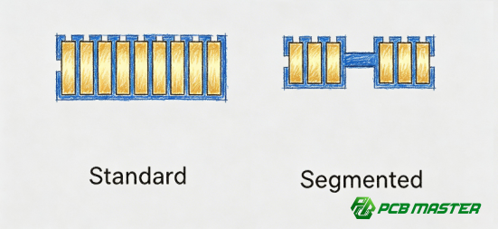
What Are the Definitions and Types of Segmented Gold Fingers?
Segmented gold fingers are edge connectors divided into different sections for selective contact. The main types are selective gold fingers and intermittent gold fingers.
l Selective Gold Fingers: These connectors have specific areas plated with gold where electrical contact is required. The non-plated areas remain bare or insulated, preventing unwanted connections. This type is common in high-precision applications like memory modules.
l Intermittent Gold Fingers: Also called “gap gold fingers,” these have repeated gold and non-gold sections along the same edge. The gaps control the sequence of electrical contact, which is useful for devices that need staged power-up or signal connections.
Example: Memory sticks use selective gold fingers to ensure power and data lines connect only in the correct positions, preventing short circuits or misalignment during installation.
What Role Do Segmented Gold Fingers Play in Circuit Connection and Function?
Segmented gold fingers control where and when a PCB connects to a device, ensuring reliable electrical performance and preventing damage.
l Precise Connection: By exposing only certain areas of the gold contacts, segmented gold fingers guide the exact points where electricity flows.
l Staged Contact: In complex devices, different segments can engage in a specific order. This allows circuits to power up sequentially, reducing current spikes.
l Signal Integrity: High-speed signals benefit from segmented gold fingers because controlled contact reduces interference and maintains consistent impedance.
Example: In a high-speed graphics card, segmented gold fingers ensure the video memory connects in a sequence that avoids data corruption during boot-up.
What Are Typical Applications of Segmented Gold Fingers?
Segmented gold fingers are used in devices that require precise, reliable PCB connections, especially where speed, density, or staged contacts matter.
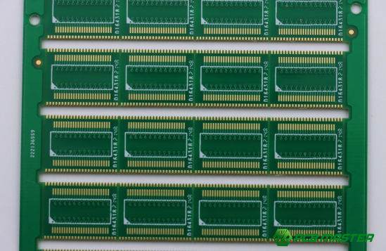
l Memory Modules (RAM): Enable selective contact for data and power pins, ensuring proper installation in motherboard slots.
l Graphics Cards: Control connections for high-speed signals and multiple power rails.
l High-Speed Communication Backplanes: Segmenting gold fingers prevents signal interference and supports complex routing for multiple channels.
l Test Sockets and Jigs: Allow staged connections for functional testing of chips or boards without damaging delicate components.
Case Study: A server-grade backplane uses segmented gold fingers to connect multiple daughter boards. The segmentation ensures that power lines engage first, followed by data lines, preventing damage and improving system reliability.
What Are the Main Manufacturing Methods for Segmented Gold Fingers?
Segmented gold fingers can be produced using several specialized methods. Each method balances precision, cost, and production volume differently. Choosing the right method depends on batch size, product complexity, and performance requirements.
Tape Masking Method (Tape Masking)
Tape masking uses adhesive tape to protect areas of the gold finger that should not be plated, making it simple and flexible for small batches.
Process Steps:
1. PCB Preparation: Complete standard PCB fabrication, including drilling, copper plating, and surface cleaning.
2. Tape Application: Skilled operators apply high-temperature, chemical-resistant tape over areas where gold is not needed.
3. Electroplating: The board is immersed in a plating solution, depositing gold only on exposed copper areas.
4. Tape Removal: Peel off the tape, revealing unplated sections.
5. Final Processing: Clean and perform any further finishing, such as tin spraying.
Advantages: Low cost for prototypes, flexible for complex patterns, easy to implement without specialized equipment.
Limitations: Precision is limited, labor-intensive, and risk of tape residue affecting quality.
Example: Small-scale memory module prototypes often use tape masking for selective gold plating.
Dry Film Masking (Dry Film Masking)
Dry film masking uses a photosensitive film to create precise plating patterns, ideal for medium to large batches.
Process Steps:
1. PCB Preparation: Complete standard PCB preparation up to copper surface readiness.
2. Film Lamination: Apply dry film over the PCB surface.
3. Exposure: Use a photomask to expose areas not requiring gold plating.
4. Development: Remove unexposed areas to expose copper for plating.
5. Gold Plating: Plate gold only on exposed copper.
6. Film Removal: Strip the remaining dry film to reveal protected areas.
Advantages: High precision, suitable for automated processes, consistent quality.
Limitations: Higher initial cost, longer setup, requires photomask.
Example: Mid-volume graphics card PCBs often use dry film masking to achieve clear segmented gold finger patterns.
Laser Ablation with Solder Mask
This method uses laser to remove solder mask precisely, allowing selective gold plating for high-reliability applications.
Process Steps:
1. PCB Base Prep: Standard copper plating and dry film exposure for circuit patterns.
2. Solder Mask Application: Cover entire board, including future gold finger areas.
3. Laser Ablation: UV or CO₂ laser removes solder mask from gold finger regions.
4. Surface Cleaning: Plasma or chemical cleaning removes carbonized residues.
5. Selective Gold Plating: Gold only deposits on exposed nickel areas.
6. Mask Removal: Strip remaining solder mask for final inspection.
Applications: Ideal for aerospace, medical devices, and high-speed backplanes.
Potential Defects & Control: Residue can cause defects; precise laser settings and thorough cleaning are essential.
Example: High-speed server backplanes use laser ablation to ensure smooth, reliable gold finger contacts.
Selective Plating with Mask (Lead Frame Masking)
This method uses a metal mask aligned over the gold finger area, enabling fast, high-precision plating for mass production.
Process Steps:
1. PCB Fixing: Secure board in production fixture.
2. Mask Alignment: Place custom metal mask over the gold finger area.
3. Electroplating: Spray or deposit gold through exposed areas only.
Advantages: Very fast, highly precise, minimal material waste.
Limitations: High initial cost, mask changes needed for new designs, suitable only for large batches.
Example: High-volume RAM production uses this method to save gold material and maintain consistent quality.
Etching Method (Plate-Then-Etch)
This method plates the entire finger and then etches away unwanted areas, useful for complex patterns.
Process Steps:
1. Full Gold Plating: Plate the whole edge with nickel and gold.
2. Photoresist Application: Protect desired gold areas using dry film or resist.
3. Etching: Chemically remove unprotected gold and nickel.
4. Resist Removal: Clean off the protective layer.
Advantages: Can produce complex patterns.
Limitations: High cost due to material waste, environmental concerns from etchants, risk of side etching affecting precision.
Example: Specialized test fixtures for chips may use this method for intricate gold finger layouts.
Comparison Table of Segmented Gold Finger Methods
Method Precision Batch Size Cost Advantages Limitations Typical Use Case Tape Masking Medium Small Low Flexible, simple Labor-intensive, residual tape Prototypes, small batches Dry Film Masking High Medium Medium Automated, precise Setup cost, photomask needed Mid-volume PCBs Laser Ablation Very High Medium-High High High reliability, fine pitch Residue, laser control required Aerospace, server backplanes Selective Plating Very High Large High initial Fast, efficient, minimal waste Mask cost, low flexibility Mass production RAM/graphics cards Etching (Plate-Then-Etch) High Small-Medium High Complex patterns Material waste, environmental impact Specialized test boards
| Method | Precision | Batch Size | Cost | Advantages | Limitations | Typical Use Case |
| Tape Masking | Medium | Small | Low | Flexible, simple | Labor-intensive, residual tape | Prototypes, small batches |
| Dry Film Masking | High | Medium | Medium | Automated, precise | Setup cost, photomask needed | Mid-volume PCBs |
| Laser Ablation | Very High | Medium-High | High | High reliability, fine pitch | Residue, laser control required | Aerospace, server backplanes |
| Selective Plating | Very High | Large | High initial | Fast, efficient, minimal waste | Mask cost, low flexibility | Mass production RAM/graphics cards |
| Etching (Plate-Then-Etch) | High | Small-Medium | High | Complex patterns | Material waste, environmental impact | Specialized test boards |
How to Control Quality and Precision in Segmented Gold Finger Production?
Maintaining high quality and precision in segmented gold fingers is essential to ensure reliable PCB performance. This involves careful control at every stage: from baseboard preparation to final testing.
How to Control Pre-Processing and Substrate Preparation?
Proper substrate preparation ensures the PCB surface is clean, flat, and ready for precise gold plating.
l Surface Cleaning: Remove dust, oils, and oxidation from copper surfaces using chemical cleaners or plasma treatment.
l Copper Thickness: Ensure consistent copper thickness across the gold finger area to support uniform plating.
l Planarity Check: Flat and smooth edges prevent uneven plating and poor electrical contact.
Example: For high-speed memory modules, a poorly prepared substrate can lead to uneven gold deposition, causing intermittent signal failure. Controlling substrate prep reduces defects from the start.
How to Manage Mask or Tape Placement Precision?
Accurate application of masks or tape ensures gold only plates the intended areas.
l Alignment Tools: Use fixtures or semi-automated tape applicators to position masking accurately.
l Edge Control: Check edges of the mask for gaps or overlaps that could allow unwanted plating.
l Operator Training: Skilled operators or automated machines reduce errors during tape or mask placement.
Example: In tape masking small batches, improper alignment can leave gold on insulated areas, leading to shorts. Using a jig can improve precision and repeatability.
How to Monitor Electroplating Parameters (Temperature, Current, Time)?
Controlling plating parameters ensures uniform thickness and high-quality gold deposition.
l Current Density: Too high can cause burning; too low leads to thin plating.
l Solution Temperature: Stable temperature avoids uneven plating or poor adhesion.
l Time Control: Over-plating wastes gold; under-plating reduces reliability.
Example: In selective plating for graphics cards, consistent current and time control ensure each gold finger segment has the same thickness, preventing uneven contact resistance.
How to Control Laser Removal and Surface Cleaning Quality?
Proper laser ablation and cleaning remove solder mask accurately without damaging the underlying nickel layer.
l Laser Calibration: Set proper power, focus, and speed to remove only the solder mask.
l Residue Removal: Use plasma or chemical cleaning to eliminate carbonized residue left by the laser.
l Inspection: Confirm exposed nickel surfaces are smooth and fully clean before plating.
Example: High-speed server backplanes use UV lasers to expose gold areas; residue left uncleaned can lead to poor adhesion or gold pitting.
How to Perform Post-Processing and Finished Product Inspection?
Final inspection ensures all gold finger segments meet mechanical and electrical standards.
l Optical Inspection: Check for plating gaps, misalignment, or surface defects using magnification or automated optical systems (AOI).
l Electrical Testing: Measure continuity and contact resistance to verify each segment works correctly.
l Final Cleaning: Remove any residues or contaminants from plating and masking steps.
Example: In high-reliability aerospace PCBs, AOI detects micro-defects that could otherwise cause intermittent failures during operation, and electrical testing confirms full connectivity before shipping.

What Are the Cost and Batch Strategy Considerations for Different Segmented Gold Finger Processes?
Selecting the right gold finger process depends on batch size, cost constraints, and production flexibility. Understanding which method fits your production scenario ensures efficiency, quality, and cost-effectiveness.
Which Processes Are Best for Small vs. Medium/Large Batches?
Some manufacturing methods are better suited for small prototypes, while others excel in high-volume production.
l Small Batches: Tape masking and etching (plate-then-etch) are ideal for small runs or prototypes. They require low initial investment and allow flexible changes in design. Manual or semi-automated methods work well here.
l Medium to Large Batches: Dry film masking, laser ablation, and selective plating are better for medium and large-scale production. These methods offer high precision, repeatability, and automated processes, reducing labor costs and improving consistency.
Example: A prototype RAM module may use tape masking for a batch of 50 units, while mass-produced graphics cards rely on selective plating with a metal mask for thousands of units.
How to Control Costs and Save Materials?
Choosing the right process and managing plating efficiency reduces material waste and production expenses.
l Selective Plating: Uses masks to deposit gold only where needed, minimizing gold waste.
l Process Optimization: Accurate control of plating time, current, and solution concentration ensures no over-plating.
l Batch Planning: Producing in larger, consistent batches reduces per-unit material and labor costs.
Example: In server backplane production, selective plating reduces gold consumption by up to 30% compared to full-edge plating, significantly lowering material costs.
How to Balance Investment, ROI, and Process Flexibility?
High-precision processes require more upfront investment but offer long-term savings and consistent quality.
l Investment vs. Volume: Methods like laser ablation or selective plating require expensive equipment, making them suitable for large-scale production with predictable demand.
l Return on Investment (ROI): The initial cost is offset by faster production, reduced waste, and higher yield rates.
l Flexibility Consideration: Tape masking or etching allows easy design changes, making them ideal for R&D and prototypes, but less cost-efficient for mass production.
Example: PCB manufacturers like PCBMASTER invest in selective plating for mass-produced RAM boards. While the upfront cost is high, ROI is achieved through material savings, speed, and uniform quality across thousands of units.
How Does PCBMASTER Provide High-Quality Segmented Gold Finger Solutions for Customers?
PCBMASTER ensures every segmented gold finger meets strict quality and performance standards. This is achieved through tailored process selection, automated production, and rigorous testing.
How Does PCBMASTER Select Processes and Offer Customer Customization?
PCBMASTER chooses the most suitable gold finger process for each project and provides flexible customization to meet client requirements.
l Process Selection: Depending on batch size, product complexity, and cost targets, PCBMASTER recommends tape masking, dry film masking, laser ablation, or selective plating.
l Customer Customization: PCBMASTER can adapt gold finger length, segment spacing, plating thickness, and layout patterns to match specific PCB designs.
l Design Consultation: Engineers review customer CAD files to optimize segment placement, avoid interference, and ensure compatibility with connectors or test fixtures.
Example: For a high-speed communication backplane, PCBMASTER may combine laser ablation with selective plating to achieve precise, dense gold finger segments that match the client’s signal integrity requirements.
How Does PCBMASTER Ensure Precision Through Automated Production?
Automated equipment and strict process control maintain high precision, consistency, and repeatability in segmented gold finger production.
l Automation: Use of CNC tape applicators, robotic plating fixtures, and laser ablation systems reduces human error.
l Process Monitoring: Real-time control of plating current, temperature, and time ensures uniform gold thickness across segments.
l Alignment and Inspection: Precision jigs and sensors guarantee mask alignment and segment placement meet design tolerances.
Example: In mass production of memory modules, automated selective plating reduces variability between boards, ensuring all gold fingers meet the required contact resistance and thickness specifications.
How Does PCBMASTER Test Finished Products and Ensure Reliability?
PCBMASTER performs thorough optical and electrical testing to guarantee gold finger quality and long-term reliability.
l Optical Inspection: Automated systems check for plating gaps, misalignment, surface defects, or over-plating.
l Electrical Testing: Continuity, contact resistance, and staged contact tests confirm every gold finger segment functions as designed.
l Reliability Assurance: Boards undergo environmental stress testing, including thermal cycling and humidity tests, to ensure performance under real-world conditions.
Example: For aerospace-grade PCBs, optical inspection combined with electrical verification ensures segmented gold fingers maintain consistent conductivity after hundreds of mating cycles, preventing system failures.

Conclusion
Segmented gold fingers are key to achieving reliable, high-performance PCBs. Precise process control, automated production, and rigorous testing ensure each gold finger delivers consistent electrical contact, durability, and efficient use of materials. Advanced techniques like laser ablation, selective plating, and dry film masking allow for both flexible prototyping and large-scale production. With years of experience, PCBMASTER applies these methods to help customers create PCBs that meet strict quality standards and perform flawlessly in memory modules, graphics cards, and high-speed backplanes.
FAQs
1. Does segmented gold finger affect PCB durability?
Segmented gold fingers do not reduce PCB durability if properly manufactured. Using precise plating, clean surface preparation, and controlled thickness ensures consistent electrical contact and mechanical strength. Advanced processes like selective plating or laser ablation maintain long-term reliability even under repeated insertion cycles.
2. Which segmented gold finger process is best for high-speed signal boards?
For high-speed signal PCBs, laser ablation with solder mask or dry film masking is ideal. These methods provide high precision, tight segment spacing, and uniform gold thickness, minimizing signal interference and maintaining low contact resistance critical for high-frequency performance.
3. How can precision be controlled in small-batch segmented gold finger production?
In small batches, tape masking or careful dry film masking is commonly used. Precision is ensured through skilled operator alignment, inspection of mask edges, and controlled plating parameters. Using fixtures or semi-automated tape applicators further reduces human error.
4. How to ensure gold plating quality after laser removal of solder mask?
After laser ablation, surface cleaning is critical. Techniques like plasma cleaning or mild chemical washes remove carbonized residue without damaging the underlying nickel. A fully clean and activated nickel surface ensures strong gold adhesion and prevents defects such as pitting or poor contact.
5. Which masking method is most cost-effective for large-scale production?
For large-volume production, selective plating with a metal mask is the most economical. Although initial tooling is expensive, it delivers high-speed plating, minimal material waste, and consistent segment quality, offering a strong return on investment for mass production.

