Common Issues in Second-Level HDI PCB Production and How to Overcome Them
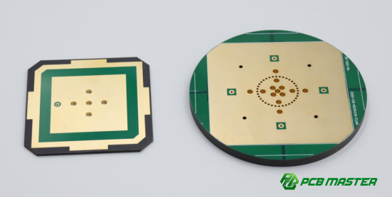
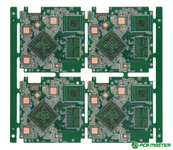
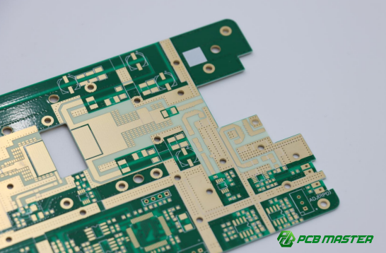
Second-level HDI (High-Density Interconnect) PCBs are crucial in today’s electronics, providing compact, high-performance solutions for devices such as smartphones, wearables, and advanced computing systems. These boards allow for more connections in a smaller space, enabling the miniaturization of circuits while maintaining functionality. However, the production of second-level HDI boards is highly complex. It involves multiple layers, precise drilling, and intricate connections, which can lead to various production challenges like alignment issues, laser drilling defects, and inconsistent plating. Ensuring reliability and performance across all these factors is critical to the final product’s success.
As an experienced PCB and PCBA supplier, PCBMASTER has developed deep expertise in tackling these challenges. Over the years, we’ve refined our processes to handle the complexities of second-level HDI production. With our advanced technology and a focus on quality control, we have successfully delivered high-performance, reliable HDI boards for a wide range of applications. In the following sections, we will explore the common issues encountered during the production of second-level HDI boards and how PCBMASTER’s solutions ensure the highest standards of quality and reliability.
Laser Drilling Common Issues and Solutions
Laser drilling common issues, such as conical or bell-shaped holes and misaligned blind vias, can be resolved by optimizing laser parameters, selecting suitable materials, ensuring clear alignment, and using high-precision drilling equipment.
Laser Hole Shape Defects: How to Improve Conical and Bell-Shaped Holes?
Issue Description:
In laser drilling, one common problem is poor hole shape, often resulting in conical (tapered) or bell-shaped holes. This defect can cause issues with plating, leading to uneven copper deposition, which in turn affects the PCB’s electrical performance and reliability.
Root Cause Analysis:
l Improper Laser Parameters: Incorrect energy settings, pulse frequency, or the number of pulses can cause irregular hole shapes.
l Material Issues: The type of PCB material, such as high-resin content or poor-quality copper, can cause uneven drilling.
l Unclear Alignment Markings: Misalignment of laser focus due to unclear or poor-quality alignment targets can cause the hole to deviate from the desired shape.
Improvement Solutions:
l Optimize Laser Parameters: Carefully adjust the laser’s energy, pulse frequency, and focus to match the material type (e.g., copper foil, resin layers). This optimization can significantly improve the hole shape and ensure consistent drilling results.
l Choose Suitable Materials: Use materials that are compatible with laser drilling, such as low-profile copper foils and resins that allow for more precise cuts.
l Ensure Clear Alignment Targets: Make sure alignment markers on the inner layers are clearly visible and placed in the correct position. This ensures the laser is focused correctly, avoiding deviations in hole shape.
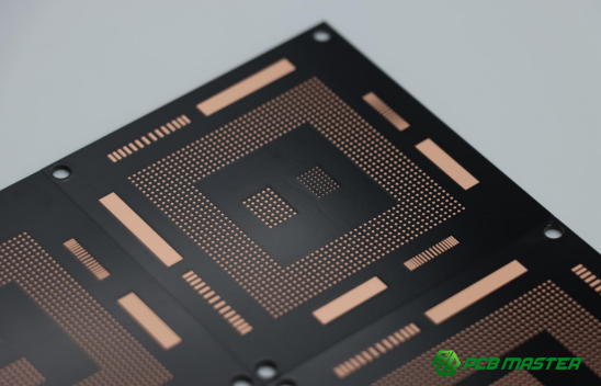
Blind Hole Alignment Issues: How to Reduce Staggered To Hole (STH) Errors?
Issue Description:
In HDI PCB manufacturing, one challenge is misalignment between the first and second-level blind vias. This misalignment can cause open circuits or poor electrical connections due to improper alignment, impacting the PCB’s functionality.
Root Cause Analysis:
l Layer Misalignment: During multi-layer lamination, inconsistent expansion or contraction of materials (e.g., prepregs and copper) leads to misalignment of the vias.
l Insufficient Drill Machine Precision: If the drilling machine lacks the necessary precision (e.g., more than ±25 microns), the alignment of blind vias across layers can be inaccurate.
l Substrate Warping: The substrate may warp or shift during the lamination process, further compounding the alignment issue.
Improvement Solutions:
l Strict Control of Material Shrinkage: Control the expansion and contraction of core materials and prepregs. Bake inner layers to reduce moisture content and pretest for shrinkage before lamination.
l Use High-Precision Laser Drilling Machines: Ensure that drilling machines have a high level of precision (e.g., ±15 microns) to guarantee proper alignment of vias across layers.
l Conformal Laser Ablation: Use conformal laser ablation to create vias on the surface before drilling, which helps maintain alignment accuracy and prevents misalignment between layers.
Electroplating and Hole Filling Common Issues and Solutions
Electroplating and hole filling issues, such as voids and copper cracking, can be solved by optimizing plating parameters, improving hole shape, using pulse plating, controlling electroplating solution purity, and selecting materials with better thermal expansion matching.
Electroplating Hole Filling Defects: How to Solve Voids and Depressions?
Issue Description:
When electroplating is performed on blind holes, sometimes the copper filling is incomplete, leaving voids or depressions in the hole. This issue affects heat dissipation and reduces the overall reliability of the PCB, especially in high-performance applications.
Root Cause Analysis:
l Electroplating Solution Issues: An imbalance in the additives (such as accelerators and suppressors) used in the electroplating solution can cause uneven copper deposition, leading to voids.
l Incorrect Electroplating Parameters: Poorly set plating parameters, like current density and waveform, can result in uneven plating that causes defects.
l Bad Hole Shape: If the hole shape is not ideal (e.g., cone-shaped or irregular), it can make it harder for the plating solution to evenly fill the hole, leading to voids or depressions.
Improvement Solutions:
l Optimize Electroplating Formulas and Parameters: Adjust the electroplating solution's additive ratio and optimize parameters such as current density and temperature to ensure uniform copper deposition.
l Strengthen Process Monitoring: Regularly monitor the electroplating process through methods like CVS (Cyclic Voltammetry Stripping) to ensure the additive concentrations remain balanced and consistent.
l Improve Hole Shape: Correcting the hole shape, ensuring it is cylindrical rather than tapered, helps in even distribution of the electroplating solution.
l Use Pulse Electroplating: Pulse plating, which alternates between current and rest phases, can improve the uniformity of copper deposition inside blind holes, reducing voids and improving filling consistency.
Copper Cracking in Vias: How to Improve Copper Reliability in Vias?
Issue Description:
Copper cracks in vias are a common issue, particularly after thermal stress tests like those involving soldering or thermal cycling. These cracks can significantly reduce the reliability of the PCB, causing failures in the electrical connection and compromising the overall performance.
Root Cause Analysis:
l Insufficient Copper Ductility: Copper that has been plated too quickly or under high current density can have poor ductility, making it more prone to cracking under thermal stress.
l Thermal Expansion Mismatch: The copper, resin, and fiberglass layers in the PCB expand and contract at different rates when exposed to heat. This mismatch in thermal expansion coefficients (CTE) can cause stress on the copper vias, leading to cracking.
Improvement Solutions:
l Control Electroplating Solution Purity: Ensure the electroplating solution is free from impurities that could reduce copper’s mechanical properties, and maintain appropriate filtration and treatment to improve the ductility of the copper.
l Optimize Electroplating Parameters: Adjust current density during electroplating to promote a smoother, more ductile copper layer. Slower deposition rates can help create a more resilient copper structure.
l Choose CTE-Compatible Materials: Select PCB materials with a better thermal expansion coefficient match between the copper and resin, reducing the stress that causes cracks in the vias. High-speed, low-loss materials often offer better thermal stability and resistance to cracking.
Lamination and Alignment Common Issues and Solutions
Lamination and alignment issues, such as delamination or misalignment, can be resolved by optimizing lamination parameters, ensuring a vacuum environment, controlling material shrinkage, using high-stability materials, and following standardized operating procedures.
Lamination Delamination or White Spots: How to Avoid Excess Resin Flow?
Issue Description:
After lamination, issues such as layer separation or excess resin flow can occur, leading to uneven layers within the PCB. This often results in weak bonding between layers or visible white spots on the board surface.
Root Cause Analysis:
l Improper Lamination Parameters: Incorrect temperature, pressure, or vacuum settings during the lamination process can cause resin to flow too much or not bond properly.
l Poor Surface Cleanliness: Contaminants or oxidation on the inner layers can prevent proper adhesion, leading to separation or inconsistent resin distribution.
l Inappropriate PP Film Selection: Using prepregs (PP film) with incorrect resin content or improper storage conditions can lead to excessive resin flow or uneven distribution during lamination.
Improvement Solutions:
l Optimize Lamination Process: Fine-tune the lamination parameters such as temperature, pressure, and time to ensure the resin flows evenly and solidifies properly, avoiding excessive resin movement.
l Ensure Vacuum Environment: Use a vacuum press to remove air pockets and contaminants from between layers, ensuring uniform resin flow and preventing separation.
l Strict Control of Incoming Materials and Storage: Properly store prepreg materials at low temperatures and monitor resin content to ensure compatibility during lamination. Pre-bake prepregs to remove excess moisture and ensure stable resin flow during lamination.
Alignment Accuracy Issues: How to Ensure Proper Alignment?
Issue Description:
Misalignment between layers can lead to inaccurate via connections or poor electrical performance. This is a critical issue, especially for HDI boards where precision is key.
Root Cause Analysis:
l Inconsistent Material Shrinkage: Different materials in the PCB, such as prepregs and core laminates, may shrink differently during the manufacturing process, leading to misalignment between layers.
l Process-Induced Stress: During the multiple stages of PCB production—such as drilling, electroplating, and lamination—stress can accumulate, affecting the precision of layer alignment.
Improvement Solutions:
l Data-Driven Shrinkage Management: Monitor and record material shrinkage across different batches of core materials and prepregs. Use this data to adjust for shrinkage compensation during the CAM (computer-aided manufacturing) process to ensure precise alignment.
l Use High-Stability Materials: Opt for core materials and prepregs with consistent shrinkage characteristics, ensuring better dimensional stability during the manufacturing process.
l Standardized Operating Procedures: Ensure that all handling, transport, and assembly of PCB layers follow strict guidelines to minimize mechanical stress and maintain alignment precision.
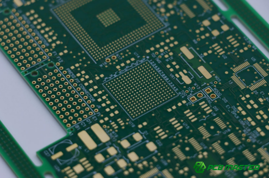
Fine Line Manufacturing Common Issues and Solutions
Fine line manufacturing issues, such as burrs and bridging, can be prevented by using MSAP or mSAP processes, upgrading exposure equipment, and optimizing etching parameters to ensure precise and accurate line production.
Challenges in Fine Line Manufacturing: How to Avoid Burrs and Bridging?
Issue Description:
When manufacturing fine lines with widths of ≤3/3mil, issues such as burrs (sharp edges) or bridging (short circuits between lines) may occur. These defects are especially problematic in high-density PCBs where precision is critical for functionality.
Root Cause Analysis:
l Low Exposure Precision: If the photolithography exposure process is not precise, it can result in misalignment, leading to gaps or bridges between lines.
l Poor Development or Etching Capability: Insufficient development or improper etching parameters can result in uneven material removal, leaving unwanted residues or creating gaps in the lines.
l Excessive Base Copper Thickness: When the base copper is too thick, it requires excessive etching to define the fine lines, increasing the likelihood of under-etching or over-etching, which can cause burrs or bridges.
Improvement Solutions:
l Adopt mSAP Processes: Using modified Semi-Additive Process (mSAP) allows for more precise control of copper thickness and the reduction of side-etching, improving the accuracy of fine lines and reducing defects like burrs and bridging.
l Upgrade Exposure Equipment: Invest in high-resolution exposure systems that can handle very fine line widths with high precision, reducing misalignment and defects.
l Optimize Etching Parameters: Adjust the etching process parameters, such as the etching time and chemical composition, to achieve more consistent and precise etching of fine lines, ensuring clear, uninterrupted circuit paths.
Comprehensive Solutions to Common Issues
Improving second-level HDI production efficiency and ensuring product consistency at PCBMASTER involves coordinated process management, precise quality control at each step, real-time monitoring, and continuous feedback to maintain high reliability and performance.
Collaborative Coordination in Second-Level HDI Production: How to Improve Overall Production Efficiency?
Improving overall production efficiency in second-level HDI manufacturing requires careful coordination across multiple stages of the process. Solving a single issue, such as laser drilling or plating defects, is not enough—each stage must work in harmony to ensure high-quality results.
Key Considerations:
l Integrated Process Management: Every step, from laser drilling to plating and lamination, must be carefully coordinated to prevent delays or errors. For example, optimizing the alignment during drilling ensures smoother lamination, reducing the risk of misalignment later in the process.
l Flow Control Between Stages: Ensuring smooth transitions between each stage can reduce bottlenecks. For example, post-drilling inspection should quickly confirm hole integrity before moving to plating, ensuring that no defects carry over to the next step.
l Cross-Department Collaboration: Close communication between departments, such as design, production, and quality control, is vital. Regular meetings and shared data can identify issues early, improving the overall production timeline and reducing errors.
By focusing on efficient coordination and cross-stage communication, manufacturers can enhance production flow and reduce the likelihood of defects that affect overall efficiency and product quality.
PCBMASTER’s Quality Control and Optimization: How to Ensure Consistency and High Reliability in Products?
At PCBMASTER, we ensure high reliability and consistency in second-level HDI production through strict quality control procedures and continuous process optimization. Each step of production is closely monitored to maintain the highest standards.
Key Quality Control Strategies:
l Precision Control at Every Step: PCBMASTER uses advanced equipment to ensure that every process—whether it's laser drilling, electroplating, or lamination—is performed with the highest precision. This ensures consistent results, reducing defects like misalignment or poor copper filling.
l Real-Time Quality Tracking: During production, PCBMASTER employs real-time monitoring tools to track the quality of each batch. This allows for immediate feedback, ensuring quick corrective actions if any deviations occur. For instance, if a plating issue is detected, the process can be adjusted before it impacts the final product.
l Continuous Feedback Loop: After production, products undergo rigorous testing and quality assessment. Feedback from these tests is integrated into the production process to further refine techniques and prevent recurring issues. This proactive approach helps maintain product consistency and reliability.
Through these meticulous quality control measures and continuous optimization, PCBMASTER ensures that every second-level HDI PCB meets the highest standards for performance and reliability.
Conclusion
The production of second-level HDI PCBs is a highly precise and challenging process that requires meticulous attention to detail and advanced technology. At PCBMASTER, we continuously optimize our techniques and processes to ensure that we provide our customers with high-quality products and exceptional service. By focusing on every stage of production, from laser drilling to plating and alignment, we guarantee reliable and consistent results. Our commitment to innovation and quality control allows us to meet the demands of the most complex PCB applications, helping our customers achieve their goals with confidence. Through ongoing improvements and a customer-centric approach, PCBMASTER stands as a trusted partner in the fast-evolving world of HDI PCB manufacturing.
FAQs
Why do conical or bell-shaped holes occur during laser drilling?
The main causes of conical or bell-shaped holes during laser drilling are improper laser parameters, mismatched material selection, and unclear alignment targets. When the laser parameters (such as energy, pulse frequency, or focus) are not optimized, it can lead to uneven hole shapes. Additionally, if the material is not suitable for laser drilling (e.g., high resin content or poor thermal conductivity), it can also result in distorted holes. Lastly, unclear or inaccurate alignment targets can cause misalignment in the drilling process, affecting hole quality and leading to these undesirable shapes.
How can the quality of electroplating hole filling be optimized?
The quality of electroplating hole filling can be improved by optimizing the electroplating formulation, adjusting the plating parameters, and employing pulse electroplating technology. By fine-tuning the additive concentrations in the electroplating solution (such as accelerators and suppressors), you can ensure more even copper deposition. Additionally, adjusting key parameters such as current density and waveform ensures better plating distribution. Using pulse electroplating helps to improve copper filling uniformity inside holes, reducing defects like voids or uneven plating.
How can interlayer alignment errors be reduced during production?
Interlayer alignment errors can be effectively reduced through digital shrinkage management, using high-stability materials, and optimizing operating procedures. By tracking material shrinkage data and compensating for it during the design and production phases, you can ensure better layer alignment. The use of stable, high-quality core materials, such as those with consistent thermal and dimensional properties, further reduces the risk of misalignment. Finally, standardized and well-documented handling and assembly processes help maintain precision across all stages, minimizing human error and mechanical stress that could affect alignment.
What are the common challenges in fine line manufacturing?
Common challenges in fine line manufacturing include poor exposure precision, side-etching during the etching process, and excessive base copper thickness. Low exposure precision can lead to misalignment or incomplete definition of the fine lines, while side-etching results from an inefficient etching process where material is removed from the sides of the lines, causing undesired gaps. Additionally, a thicker base copper layer requires excessive etching to define narrow lines, which increases the risk of under-etching or over-etching. These issues can be addressed by optimizing process parameters such as exposure, etching time, and copper thickness.
How does PCBMASTER address the challenges in second-level HDI board production?
PCBMASTER addresses the challenges in second-level HDI board production by maintaining precise process control, selecting suitable materials, and optimizing production workflows. Through advanced techniques like fine-tuned laser drilling, precise electroplating, and accurate alignment, PCBMASTER ensures the production of high-reliability HDI boards. We also continuously monitor and adjust our processes, ensuring that each step—from material preparation to final testing—meets strict quality standards. Our commitment to innovation and process improvement ensures the consistency and performance of every product we deliver to our clients.