


How to Become a PCB Design Engineer: Essential Guide for Beginners
Becoming a PCB Design Engineer opens doors to a dynamic and in-demand career in the world of electronics. As devices continue to get smaller and more advanced, the role of PCB design engineers becomes even more crucial in shaping the future of technology. From consumer gadgets to cutting-edge medical equipment, the work of a PCB designer is foundational to almost every electronic device we use today.
Whether you’re passionate about electronics or looking to pivot into a technical career, this guide will walk you through the essential steps to becoming a successful PCB Design Engineer. From the skills you'll need to the tools you should master, this article will provide a roadmap for anyone looking to dive into the world of PCB design. With the right education, hands-on experience, and the right mindset, you can carve out a rewarding career in one of the most exciting and evolving fields in engineering.
Ready to get started? Let’s explore what it takes to step into the world of PCB design and launch your career in this fast-growing industry.
What is a PCB Design Engineer?
A PCB Design Engineer is a specialized professional who designs the layout of printed circuit boards (PCBs) that power and connect the components in electronic devices. They play a critical role in creating the backbone of almost every electronic gadget, from smartphones to medical equipment, ensuring that the electrical connections are efficient and reliable.
Role of a PCB Design Engineer
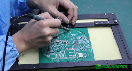
The primary responsibility of a PCB Design Engineer is to design the physical layout of a circuit board. This involves creating a detailed map of how electronic components like resistors, capacitors, and microchips are arranged and connected. The engineer uses design software to translate a circuit diagram into a real-world PCB layout, ensuring the design is both functional and manufacturable.
In addition to the design process, PCB Design Engineers also work closely with hardware engineers, manufacturers, and quality control teams to test and validate the designs. They ensure that the PCBs can handle the required electrical signals and meet industry standards for durability and performance.
Importance of PCB Design Engineers in the Electronics Industry
PCB Design Engineers are crucial in today's fast-paced electronics industry because nearly every electronic product relies on PCBs to function. From consumer electronics like smartphones to advanced medical devices and automotive systems, PCBs are at the heart of modern technology.
Their designs directly impact the quality, performance, and reliability of the final product. For example, in smartphones, the efficiency of the PCB design affects the battery life, processing power, and overall user experience. In medical equipment, it can determine how accurately devices function, potentially saving lives.
Real-World Example: Smartphone PCB Design
Take, for example, a smartphone PCB design. A PCB Design Engineer must ensure that the tiny board is able to handle multiple complex circuits, including those for the camera, screen, and wireless communication. By optimizing the layout, they can improve signal quality, reduce energy consumption, and prevent overheating, all of which are critical for the phone's performance.
What Skills Do You Need to Become a PCB Design Engineer?
Becoming a PCB Design Engineer requires a combination of technical skills and soft skills. These skills help engineers create high-quality PCB layouts and work effectively in teams to design and manufacture electronic devices. Let's explore the key skills needed for this role.
Technical Skills
To become a successful PCB Design Engineer, you need to have strong technical skills in the following areas:
1. PCB Design Software
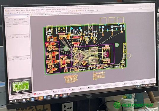
PCB design engineers use specialized software tools to create the layouts for circuit boards. Popular tools include Altium Designer, Eagle, and KiCad. These tools help engineers draw the PCB schematic, layout the board, and run simulations to ensure the design will work correctly. Learning how to use these software programs is essential for anyone entering the field.
Real-World Example: A PCB design engineer using Altium Designer might create a high-speed circuit for a smartphone’s communication system. The software allows them to optimize the layout to ensure fast data transfer and minimal signal interference.
2. Circuit Theory
PCB Design Engineers need to understand circuit theory, which covers how electrical components interact and how current flows through a circuit. This knowledge helps engineers design boards that are both efficient and functional. Without a solid understanding of electrical concepts like voltage, current, and resistance, it would be impossible to create effective PCB layouts.
3. CAD Tools
Computer-Aided Design (CAD) tools are used to create detailed visual representations of PCB layouts. These tools allow designers to manipulate the placement of components, conduct simulations, and ensure that the design can be successfully manufactured. CAD software helps create accurate and precise blueprints for PCBs, reducing errors in the production process.
Real-World Example: Using CAD tools, a PCB engineer might design a multi-layer PCB for a medical device, ensuring the board fits in a small, compact case while maintaining optimal performance.
Soft Skills
While technical expertise is essential, soft skills also play a critical role in a PCB Design Engineer's success. Here are a few key soft skills needed for this profession:
1. Attention to Detail
PCB design is all about precision. A small mistake in the placement of a component or a wrong connection can render the entire circuit useless. PCB Design Engineers must be able to focus on the smallest details and ensure that every element is accurately placed according to the design specifications.
Real-World Example: A small mistake in the routing of traces on a PCB could cause an electrical short or signal interference. Attention to detail ensures these types of errors are avoided during the design phase.
2. Team Collaboration
PCB Design Engineers often work in teams with other engineers, product designers, and manufacturers. Effective communication and collaboration are essential to ensure that designs meet the requirements of the project. Engineers must be able to understand input from other team members and incorporate it into the design process.
Real-World Example: A PCB Design Engineer working on a wearable device must collaborate with product designers to ensure that the PCB fits within the limited space of the device, while still delivering the required performance.
3. Problem-Solving
During the design and testing phases, engineers often face challenges related to component placement, signal integrity, or manufacturing constraints. PCB Design Engineers need to be good problem solvers who can quickly identify issues and come up with solutions to fix them.
Real-World Example: A PCB Design Engineer working on a drone’s flight controller might encounter signal interference between components. Using problem-solving skills, they can rearrange the layout or add shielding to resolve the issue and ensure the drone operates smoothly.
What Education is Required for PCB Design Engineering?
Becoming a PCB Design Engineer typically requires a combination of formal education and additional certifications. Here's a breakdown of the key educational requirements for entering this field.
Academic Background: Bachelor's Degree in Electrical Engineering or a Related Field
The foundation for a career in PCB Design Engineering usually starts with a bachelor's degree in electrical engineering, electronics, or a closely related field. This degree equips you with the essential knowledge needed to understand how electronic components work and how to design circuits effectively.
During a bachelor's program, you'll study subjects like circuit theory, digital electronics, microelectronics, and signal processing. These courses help you understand the fundamental principles that govern PCB design, such as voltage, current, and resistance, as well as how to manage power flow in circuits. Understanding these concepts is vital because PCB Design Engineers must ensure that the components on a board work together without causing electrical failures.
Real-World Example: A student with a bachelor's degree in electrical engineering may spend time working on designing simple circuits and then gradually advance to creating complex PCB layouts as part of their coursework or projects.
Additional Certifications: PCB Design Tools and Specialized Courses
While a bachelor's degree provides a solid base, additional certifications can enhance your skills and improve your job prospects. For example, mastering popular PCB design tools like Altium Designer, Eagle, or KiCad can make you a more competitive candidate. These certifications demonstrate to employers that you are proficient in industry-standard software, which is crucial in the design process.
You can find many online platforms offering certification courses in PCB design tools. Some programs even provide specialized training in high-frequency PCB design, RF circuits, or multi-layer PCB design, which are particularly useful in industries like telecommunications, aerospace, and medical devices.
Real-World Example: A PCB Design Engineer with an Altium Designer certification might be hired by a company that specializes in consumer electronics, where they would use the software to design high-performance PCBs for smartphones or laptops.
How to Gain Experience in PCB Design?
Gaining hands-on experience is crucial to becoming a proficient PCB Design Engineer. There are several ways to acquire experience, each offering unique benefits. Here's how you can build your experience in PCB design.
Internships and Entry-Level Positions: Gaining Practical Experience
Internships and entry-level positions are one of the best ways to gain practical experience in PCB design. These roles allow you to work alongside experienced engineers, learn industry-specific techniques, and apply what you’ve learned in a real-world setting. Internships also provide valuable networking opportunities, which can lead to full-time job offers.
In an internship, you may start by assisting senior engineers with basic tasks, such as component placement or checking design files for errors. Over time, you’ll gain more responsibility, working on complete PCB designs or even collaborating on larger projects.
Real-World Example: A PCB Design Engineer intern at a consumer electronics company might initially help with testing designs, then progress to designing parts of the PCB for a new product, such as a smartwatch, under the supervision of more experienced engineers.
Personal Projects and Portfolios: Showcasing Your Work
Building a portfolio of personal projects is another great way to gain experience and demonstrate your skills. Platforms like GitHub are perfect for showcasing your PCB designs. You can upload your designs, share your thought process, and even get feedback from the community.
Starting with simple projects, like designing a PCB for a basic LED circuit, and gradually moving on to more complex designs (such as a microcontroller-based system), helps you build a practical portfolio. This portfolio becomes a powerful tool when applying for jobs, as it shows employers that you can work independently and tackle design challenges.
Real-World Example: A PCB design enthusiast might upload their designs for a custom drone flight controller on GitHub, showing detailed schematics, PCB layouts, and how the design works. This can impress potential employers who are looking for hands-on experience.
Continued Learning and Skill Development: Staying Up-to-Date
PCB design is a field that evolves rapidly with new tools, technologies, and industry standards. To stay competitive, it’s essential to continuously improve your skills. Online courses, forums, webinars, and community events are excellent ways to stay updated and learn new techniques.
Taking online courses on platforms like Coursera, Udemy, or LinkedIn Learning can help you deepen your understanding of PCB design tools, advanced design techniques, and emerging trends. Participating in online communities and attending industry conferences will also allow you to network with other professionals, share knowledge, and learn from the experiences of others.
Real-World Example: A PCB Design Engineer might take an advanced course on high-frequency PCB design to improve their ability to design for 5G applications, which is an emerging trend in the telecom industry.
What Are the Challenges and How to Overcome Them?
PCB design is a complex and challenging field, requiring engineers to navigate technical obstacles, manage cost constraints, and stay updated with rapidly evolving technology. Below, we’ll explore the main challenges and how to overcome them.
Technical Challenges: Designing Complex Circuits and Multi-Layer PCBs
One of the most significant technical challenges in PCB design is handling complex circuits and multi-layer PCBs. As electronics become more advanced, designs need to accommodate more components in smaller spaces. This leads to problems with signal integrity, power distribution, and heat dissipation.
For example, when designing a multi-layer PCB, you have to ensure that the layers are correctly routed, minimizing cross-talk (interference between signals) and ensuring proper grounding. Additionally, managing trace width and spacing becomes critical for high-speed circuits to avoid signal delays or power loss.
How to Overcome It:
The key to overcoming these challenges is careful planning. Use advanced design simulation tools (such as Altium Designer or Cadence) to test and optimize your designs before manufacturing. Incorporating best practices for high-speed routing, such as using controlled impedance for traces and minimizing via connections, can significantly improve circuit performance.
Real-World Example: When designing a PCB for a high-speed communication device like a router, engineers must account for signal interference and maintain proper layer stacking. Using simulation software helps ensure that the signals reach the correct destinations without degradation.
Manufacturing and Cost Control: Optimizing Design Within Budget and Manufacturing Constraints
Another major challenge in PCB design is balancing the cost and manufacturing limitations. Designers must create efficient and functional PCBs while keeping costs within budget. This is especially challenging when working with limited resources or when designing for mass production.
For example, designing a PCB with more layers or complex components might increase the cost due to longer production times, higher material costs, or more expensive testing procedures.
How to Overcome It:
To manage costs, PCB Design Engineers must understand the manufacturing process and material costs. Using fewer layers, opting for standard components, and minimizing the use of custom parts can help reduce expenses. Additionally, designing with DFM (Design for Manufacturing) principles in mind ensures that the design is easy to produce and minimizes potential issues during manufacturing.
Real-World Example: In consumer electronics, a PCB for a budget smartphone needs to be cost-effective while maintaining performance. The engineer might limit the number of layers and choose affordable, readily available components, all while ensuring the design remains functional.
Rapidly Evolving Industry: Adapting to Changing Technologies
The field of PCB design is constantly evolving, driven by innovations in technology and new requirements from industries like 5G, IoT (Internet of Things), and wearables. For instance, PCB designs for 5G devices need to handle higher frequencies and higher data rates than previous technologies, requiring engineers to update their skills and knowledge regularly.
How to Overcome It:
Staying up-to-date with industry trends is crucial for PCB Design Engineers. Continuously learning through online courses, industry webinars, and conferences helps engineers keep pace with new technologies. Additionally, experimenting with new tools and techniques, such as high-frequency design principles or flexible PCBs, can help engineers remain competitive.
Real-World Example: As 5G technology rolls out, PCB Design Engineers need to understand how to design boards that can handle higher frequencies and tighter signal tolerances. Taking specialized courses in RF (Radio Frequency) design allows engineers to tackle the challenges posed by new wireless standards.
Conclusion
The career prospects for PCB Design Engineers are bright, with growing demand in industries like consumer electronics, automotive, healthcare, and telecommunications. As technology advances, the need for more sophisticated PCBs to support innovations like 5G, IoT devices, and wearable technology continues to rise. This growth creates opportunities for engineers to specialize in areas such as high-frequency PCB design, multi-layer PCB development, and advanced manufacturing processes.
For those looking to enter the field or take their careers to the next level, companies like PCBMASTER offer a great example of what’s possible. As an experienced PCB and PCBA supplier, PCBMASTER has a team of skilled senior PCB design engineers who ensure the delivery of high-quality products tailored to client needs. With expertise in both the design and manufacturing aspects of PCBs, PCBMASTER is well-positioned to support companies looking to create reliable, cutting-edge electronic products.
By pursuing a career in PCB design, engineers can tap into a rewarding and dynamic field with plenty of room for growth and specialization. Whether working for a company like PCBMASTER or starting their own venture, the opportunities in this sector are vast and full of potential.
FAQs
How long does it take to become a PCB Design Engineer?
Becoming a PCB Design Engineer typically takes around 4 years if you're pursuing a bachelor's degree in electrical engineering or a related field. After completing your degree, gaining practical experience through internships or entry-level positions may take an additional 1-2 years. With continuous learning and on-the-job training, you can become proficient in PCB design in about 3-5 years.
Can I become a PCB Design Engineer without a degree?
Yes, it’s possible to become a PCB Design Engineer without a formal degree, though it may be more challenging. Many engineers in this field have built their careers through self-study, certifications, and hands-on experience. Learning PCB design tools like Altium or Eagle, completing online courses, and building a personal portfolio of designs on platforms like GitHub can help you demonstrate your skills and gain employment in the field.
How much do PCB Design Engineers earn?
The salary of a PCB Design Engineer varies depending on experience, location, and industry. On average, entry-level PCB designers earn around $50,000 to $70,000 per year. With experience, mid-level engineers can make between $70,000 to $100,000, and senior engineers can earn $100,000 to $130,000 or more, especially in high-demand sectors like telecommunications and aerospace.
What is the best way to start learning PCB design?
The best way to start learning PCB design is by getting hands-on experience. Begin by learning the basics of electronics and circuit theory, then move on to PCB design software like KiCad or Eagle. You can find free tutorials and courses online to help you understand the design process. Building small projects like simple LED circuits or Arduino-based designs will help you apply what you’ve learned and build a portfolio.
Is PCB Design Engineering a good career choice in 2026?
Yes, PCB Design Engineering is expected to remain a strong career choice in 2026. As technology continues to advance, the demand for more sophisticated and reliable PCBs will grow. Industries like 5G, IoT, and autonomous vehicles will create new opportunities. With a shortage of skilled engineers, those with expertise in PCB design will likely be in high demand, making it a promising field for the future.


