RF PCB Design: The Ultimate Guide to High-Performance Circuit Boards
RF PCB design plays a critical role in the performance of modern electronic devices, especially in wireless communication technologies. With the rise of 5G, IoT, and other advanced wireless systems, high-frequency circuit boards have become essential for ensuring stable and reliable communication. RF PCBs are designed to handle radio frequency signals, which travel through the air and require precise control to maintain signal integrity and minimize interference.
This guide is crafted to provide you with a clear understanding of RF PCB design, offering practical tips and techniques that are essential for creating high-performance boards. From selecting the right materials to optimizing layout and managing thermal performance, this guide covers the key aspects that directly impact the performance of RF PCBs in real-world applications. Whether you’re working on mobile devices, wireless routers, or other RF-based systems, mastering these principles will help you design better, more efficient PCBs that support advanced technologies with confidence.
What is RF PCB Design and Why is it Critical?
Definition of RF PCB Design
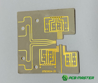
RF PCB design refers to the process of creating printed circuit boards specifically designed to handle radio frequency (RF) signals. These signals are electromagnetic waves that carry information across devices, and they are used in wireless communication systems. RF PCBs are different from standard PCBs because they are designed to minimize signal loss, reduce interference, and ensure that high-frequency signals travel efficiently through the board. This is crucial in modern electronics, where fast, reliable communication is key for devices like smartphones, routers, and medical equipment.
Applications of RF PCBs
RF PCBs are used in a wide range of electronic devices that require high-frequency signal transmission. Some common applications include:
Smartphones: RF PCBs are integral to mobile phones, handling the signals for cellular connections, Wi-Fi, and Bluetooth.
Wireless Routers: These devices rely on RF PCBs to manage wireless communication between the router and connected devices.
Medical Devices: RF technology in medical devices, such as MRI machines and wireless sensors, requires highly reliable RF PCBs for accurate signal processing.
Radar Systems: RF PCBs are used in radar systems for monitoring and detecting objects at high frequencies, such as in air traffic control and military applications.
RF PCB Design vs. Standard PCB Design
RF PCBs differ from traditional, or "standard," PCBs in several key areas, primarily because of the frequencies they handle and the need for precise signal integrity. Here's a simple comparison:
| Feature | RF PCB Design | Standard PCB Design |
| Frequency Handling | Designed to manage high-frequency signals (typically above 100 MHz). | Handles lower-frequency signals (typically below 100 MHz). |
| Signal Integrity | Emphasis on minimizing signal loss, reflection, and crosstalk. | Focus is on general electrical connections without significant concern for signal degradation. |
| Component Layout | Requires precise component placement to minimize interference and maximize performance. | Component placement is more flexible, with fewer considerations for interference. |
| Material Choice | Uses specialized materials like PTFE or ceramic to reduce loss and maintain signal quality. | Generally uses standard materials like FR4, which are sufficient for low-frequency designs. |
| Trace Width & Spacing | Critical for impedance matching and minimizing signal loss. | Trace width and spacing are less critical for standard designs. |
How Do RF Circuit Boards Achieve High Performance?
RF circuit boards achieve high performance by ensuring signal integrity through impedance matching and minimizing transmission line loss, while also managing heat dissipation using thermal vias and heat sinks.
Signal Integrity in RF Designs
Signal integrity is crucial in RF circuit boards because high-frequency signals are more susceptible to interference, distortion, and loss as they travel through traces. Maintaining signal quality means ensuring the signals arrive at their destination without significant degradation, which is key for reliable performance. To achieve this, RF PCB designers must focus on minimizing signal loss, reflection, and crosstalk.
- Impedance Matching: One of the most important techniques for maintaining signal integrity is impedance matching. When signals travel through a PCB, they encounter varying impedances at different points, which can cause reflections (signal bounce) that distort the original signal. To prevent this, the impedance of the PCB traces must match that of the components and connectors they are connected to. This can be achieved by adjusting trace widths, using specific materials, and ensuring that the routing does not cause abrupt changes in impedance.
- Minimizing Transmission Line Loss: Transmission line loss occurs when signals lose energy as they travel along traces. In RF designs, this can significantly reduce signal strength and affect performance. To minimize this loss, designers use low-loss materials like PTFE (Teflon) and ceramics, which reduce energy dissipation. Additionally, optimizing trace width and spacing, and avoiding long, thin traces, can help reduce transmission line losses.
Thermal Management in RF PCBs
Thermal management is essential in RF PCB design because high-frequency circuits generate heat during operation. If the heat isn’t effectively managed, it can lead to component failure, degraded performance, or even complete circuit failure. Proper thermal management helps maintain the performance and longevity of RF PCBs.
- Use of Thermal Vias and Heat Sinks: To address heat dissipation, designers often use thermal vias and heat sinks. Thermal vias are special holes drilled into the PCB that allow heat to pass from the component’s surface to the backside or inner layers of the PCB, helping to spread the heat evenly. These vias are typically filled with copper to provide a conductive path. Heat sinks, which are metal components attached to hot parts of the PCB, help draw heat away from sensitive areas. By using both thermal vias and heat sinks strategically, designers can ensure that the temperature of the PCB remains within safe limits, even during high-performance operation.
What Are the Key Materials for RF PCB Design?
The key materials for RF PCB design include substrates like FR4, PTFE, and ceramic, copper thickness for impedance control, and dielectric materials with low, stable dielectric constants to ensure high-frequency performance and minimal signal loss.
PCB Substrates for RF Design
The substrate is the foundational material that makes up the body of a PCB. For RF design, the choice of substrate is critical because it impacts the performance of the high-frequency signals passing through the board. Common RF PCB substrates include:
- FR-4: The most commonly used material for general PCBs, FR4 is affordable and widely available. However, it has limitations when it comes to high-frequency applications because it has a higher loss at RF frequencies.
- PTFE (Teflon): Known for its low loss and stable dielectric properties, PTFE is a popular choice for high-frequency applications. It offers excellent performance in reducing signal attenuation and maintaining signal integrity at RF frequencies.
- Ceramic Substrates: These materials are used for specialized RF applications that demand very high performance. They offer superior thermal conductivity and low dielectric loss, making them ideal for demanding RF designs like those used in aerospace and military equipment.
High-Density Interconnect (HDI) Materials
HDI materials are designed to provide higher performance in compact designs by enabling smaller, denser layouts. For RF designs, HDI PCBs offer benefits like reduced signal path lengths and improved signal integrity. By utilizing microvias and fine trace widths, HDI materials reduce the effects of parasitic inductance and capacitance, ensuring that high-frequency signals remain sharp and undistorted. This makes HDI particularly beneficial for applications like smartphones, which need to handle multiple high-frequency signals in a small space.
Copper Thickness and Its Impact on Performance:Copper thickness in an RF PCB directly influences its electrical performance, particularly in terms of impedance control and conductivity. Thicker copper traces have lower resistance, which helps maintain signal strength and minimize power loss. However, increasing copper thickness can also affect the impedance of the traces, which can lead to signal integrity issues if not carefully managed. The key is to select the right copper thickness based on the signal frequency, trace width, and desired impedance characteristics. For example, high-frequency designs often benefit from thinner copper layers to control impedance more precisely.
Dielectric Materials
The dielectric material in a PCB influences how signals propagate through the traces. The dielectric constant (also called relative permittivity) of the material determines how the electromagnetic wave is slowed down as it travels through the PCB. Lower dielectric constants are typically preferred for RF applications because they allow for faster signal transmission with less distortion. When selecting dielectric materials, designers need to choose ones with a consistent and low dielectric constant to ensure that the signal velocity is predictable and stable. Materials like PTFE and ceramic offer low, stable dielectric constants, which are crucial for maintaining high performance in RF circuits.
What Are the Best Practices for Routing RF Circuits?
The best practices for routing RF circuits include carefully calculating trace width for impedance matching, minimizing via usage to reduce signal loss, and designing an optimal multi-layer stack-up with internal ground planes to improve signal integrity and reduce EMI.
Trace Width and Spacing
In RF PCB design, trace width and spacing are critical for achieving proper impedance matching and minimizing signal degradation. Impedance matching ensures that signals travel through the PCB without reflections, which can distort the signal. To calculate the ideal trace width, you need to consider factors like the PCB's dielectric material, the trace's thickness, and the desired impedance (typically 50 ohms for most RF applications). A wider trace reduces the impedance, while a narrower trace increases it. The spacing between traces also plays a role in preventing crosstalk—the unwanted interference caused by signals bleeding from one trace to another. Proper trace width and spacing are essential to maintain signal clarity and prevent performance issues in high-frequency circuits.
Minimizing Via Usage
Vias, which are small holes that connect different layers of a PCB, are necessary for multi-layer designs, but they can negatively affect RF performance. Each via introduces inductance and resistance, which can slow down signal transmission and increase signal loss. Additionally, vias can cause reflections and impedance mismatches, especially when used in high-frequency circuits. To minimize the impact, try to reduce the number of vias by designing a more efficient layer stack-up or using microvias. When vias are necessary, keep them as short and small as possible to reduce their adverse effects on signal integrity.
Optimal Layer Stack-Up for RF PCB
For high-frequency applications, designing a multi-layer PCB with the right layer stack-up is crucial for maintaining signal integrity. The layer stack-up refers to the arrangement of different layers (such as signal layers, power planes, and ground planes) in the PCB. To ensure that signals travel cleanly, the signal layers should be placed between ground planes to create a controlled impedance environment. This layout helps to reduce noise and crosstalk, improving overall signal quality. Additionally, using a carefully planned stack-up allows for better control of the electrical properties of the PCB, making it easier to meet the high-performance requirements of RF circuits.
Internal Ground Planes: One key element of an optimal layer stack-up is the use of internal ground planes. These ground planes provide a low-impedance path for signals, reducing noise and minimizing electromagnetic interference (EMI) . Ground planes also help to shield sensitive components from external interference, improving the overall performance of the RF circuit. By placing internal ground planes close to the signal traces, you can enhance signal integrity, ensuring that high-frequency signals pass through the board with minimal distortion.
How Can You Overcome Common Challenges in RF PCB Design?
Common challenges in RF PCB design can be overcome by using effective shielding and grounding to reduce EMI, designing stable power rails for power integrity, and optimizing trace materials and layout to minimize high-frequency signal loss.
Dealing with Signal Interference and EMI
Electromagnetic interference (EMI) can significantly impact the performance of RF PCBs, leading to distorted signals, decreased reliability, and failure to meet communication standards. To reduce EMI, designers use several techniques:
- Shielding and Grounding: Shielding involves enclosing sensitive components or sections of the PCB with conductive materials (like copper or aluminum) to block external electromagnetic fields. Ground planes play a vital role in grounding the signals, providing a path for noise to escape. Properly placed ground planes reduce the noise that can interfere with the signal. It's crucial to ensure that the ground plane is continuous and solid, with no gaps or unnecessary cuts, to maintain effective noise reduction.
In addition, using copper pour (a large area of copper covering a section of the PCB) connected to the ground can help reduce EMI by providing a path for unwanted signals to dissipate. The strategic use of shielding enclosures around critical RF components can also minimize the impact of external noise, ensuring cleaner signal transmission.
Addressing Power Integrity Issues
Power integrity is essential for RF PCB designs because any fluctuation or noise in the power supply can directly affect the performance of the RF circuit. To ensure stable power delivery:
- Designing Stable Power Rails: One of the most important steps is to design well-regulated power rails that provide a constant voltage to the RF components. This can be achieved by using low-noise voltage regulators and ensuring that the power distribution network (PDN) is optimized to handle current demand efficiently.
- Decoupling Capacitors: Adding decoupling capacitors close to the power pins of components helps filter out noise and smooth power delivery. These capacitors absorb power surges and provide a stable voltage, preventing power fluctuations from affecting signal quality.
- Good Layout Practices: It's essential to place power and ground planes in a way that minimizes interference between them. Keeping the ground plane solid and low-impedance, while keeping the power distribution well-optimized, can minimize noise and ensure consistent power delivery to sensitive RF components.
Challenges with High-Frequency Signal Loss
At higher frequencies, signal loss (also known as attenuation) becomes a significant concern. As signals travel through PCB traces, some of their energy is lost due to resistance, especially at high frequencies. To overcome this challenge:
- Use of Low-Loss Materials: Choosing the right PCB material with low dielectric loss is essential to maintain signal integrity. Materials like PTFE (Teflon) and ceramics have lower loss factors, helping maintain the strength of the signal over long distances.
- Optimizing Trace Design: Reducing the length of traces, using wider traces, and ensuring consistent impedance matching across the design can minimize the chances of signal loss. For high-frequency designs, it's also important to keep the traces as short and direct as possible to avoid unnecessary attenuation.
- Using Microstrip or Stripline Structures: In RF PCB design, using microstrip or stripline trace structures (where the signal trace is either on the surface or sandwiched between the dielectric layers) helps manage signal propagation more efficiently, reducing loss and ensuring fidelity at higher frequencies.
How Do You Validate the Performance of RF PCBs?
The performance of RF PCBs is validated using simulation tools for predicting signal behavior and thermal distribution, followed by prototype testing with techniques like insertion loss, return loss measurement, and Vector Network Analyzer (VNA) to confirm signal integrity and power handling.
Simulation Tools for RF PCB Design
Simulation tools are essential in RF PCB design because they allow engineers to test and refine their designs before physical fabrication, saving time and resources. These tools model the electrical and mechanical behavior of the PCB, providing insights into how the design will perform in real-world conditions. By simulating the behavior of signals and thermal distribution, engineers can detect issues such as signal integrity problems, impedance mismatches, and excessive heat buildup early in the design process.
- Electromagnetic Simulation: Electromagnetic (EM) simulation tools are specifically designed to predict the performance of RF circuits. These tools model the electromagnetic fields and wave propagation across the PCB, helping to identify potential issues like signal reflections, interference, and losses. By simulating the design’s electromagnetic behavior, engineers can adjust the layout to ensure optimal signal integrity and reduce the impact of electromagnetic interference (EMI). For instance, tools like Ansys HFSS or CST Studio Suite can simulate high-frequency circuits to verify that signals will propagate through the PCB without distortion or loss.
Prototype Testing and Measurement
Once the RF PCB design has been simulated, the next step is to validate its performance through real-world testing. Prototype testing involves creating a physical version of the PCB to measure key parameters like insertion loss, return loss, and power handling capabilities. These parameters are critical to ensuring that the PCB will perform reliably in its intended application.
- Insertion Loss measures the loss of signal power as it passes through the PCB. Lower insertion loss indicates better signal retention.
- Return Loss quantifies the amount of signal reflected back towards the source, with higher return loss indicating better impedance matching and less reflection.
- Power Handling refers to the PCB’s ability to handle high power levels without degrading signal quality or causing damage to the components.
Vector Network Analyzers (VNA)
One of the most powerful tools for testing RF PCBs is the Vector Network Analyzer (VNA). A VNA measures the network parameters of an RF circuit, such as S-parameters (scattering parameters), which describe how signals are transmitted and reflected through the PCB. The VNA can provide detailed information about insertion loss, return loss, and the overall frequency response of the circuit. By using a VNA, engineers can confirm that the impedance is matched correctly, identify any areas with signal loss, and verify that the PCB will operate efficiently at the desired frequency. VNAs are crucial for ensuring the quality and performance of RF PCBs, particularly in high-frequency applications like 5G devices, wireless communication systems, and radar equipment.
Conclusion
RF PCB design involves key aspects such as maintaining signal integrity, managing thermal performance, and selecting the right materials like PTFE and ceramics. We've covered best practices for routing RF circuits, minimizing signal loss, ensuring power integrity, and overcoming common challenges such as electromagnetic interference (EMI). Each of these elements plays a crucial role in ensuring that RF PCBs function reliably in high-frequency applications, such as wireless communication and radar systems.
To create high-performance RF circuits, it's essential to apply these best practices throughout the design process—whether it's simulating signal behavior, minimizing via usage, or using optimal materials. Paying attention to trace width, grounding, and thermal dissipation will help reduce signal degradation and interference, ensuring efficient and reliable operation.
For those looking for a trusted partner in PCB and PCBA solutions, PCBMASTER stands out as a seasoned supplier . With years of experience, PCBMASTER is committed to providing high-quality, reliable products, ensuring that your RF PCB designs are manufactured to the highest standards of precision and performance.
FAQs
1. How does the choice of PCB material affect RF performance at different frequencies?
The choice of PCB material is crucial in RF design because the dielectric properties of the material affect signal integrity. At high frequencies, materials like PTFE (Teflon) and ceramic offer lower dielectric losses and more stable dielectric constants than standard FR4. This helps minimize signal attenuation and ensures the signals maintain their strength over long distances. For lower-frequency applications, FR4 can be sufficient, but for high-performance RF circuits, specialized materials are recommended to reduce signal degradation and interference.
2. What are the common sources of noise in RF PCB designs and how can they be minimized?
Common sources of noise in RF PCB designs include electromagnetic interference (EMI), crosstalk between traces, and power supply noise. EMI can be reduced by implementing proper shielding and ensuring a solid ground plane. Crosstalk can be minimized by increasing trace spacing and ensuring good impedance matching. Power supply noise can be mitigated with decoupling capacitors and low-noise voltage regulators. Good layout practices, such as separating sensitive signal paths from noisy power traces, are essential for minimizing noise in RF circuits.
3. Why is signal reflection a problem in RF PCB design and how can it be avoided?
Signal reflection occurs when there is a mismatch in impedance between the signal trace and its components, causing part of the signal to be reflected back towards the source. This can distort the signal and reduce overall system performance. To avoid signal reflection, it’s crucial to match the impedance of the traces with the components (such as connectors and antennas), use proper trace width calculations, and ensure that the trace routing is as short and direct as possible. Simulation tools can help identify and correct impedance mismatches before fabrication.
4. How can I optimize the use of vias in RF PCB designs to improve signal quality?
Vias, while necessary for multi-layer PCBs, can negatively affect RF signal quality due to their inductance and resistance. To optimize via usage, limit the number of vias by designing a compact layout with fewer layer transitions. When vias are needed, use microvias, which are smaller and have lower inductance compared to traditional vias. Additionally, ensure vias are as short and direct as possible to minimize signal degradation. Using via-in-pad designs and optimizing via placement helps reduce the impact on signal integrity.
5. How can I verify the performance of my RF PCB before fabrication?
Before fabrication, you can verify the performance of your RF PCB using electromagnetic (EM) simulation tools, such as Ansys HFSS or CST Studio, to model how the RF signals will behave on the PCB. These tools help identify issues like signal loss, impedance mismatches, and potential sources of interference. After simulation, you can prototype the PCB and use a Vector Network Analyzer (VNA) to measure key parameters such as insertion loss, return loss, and frequency response. This ensures that the design performs as expected before moving to mass production.
About the Author

Carol Luo
PCB Design EngineerI'm Carol, a PCB Engineer at PCBMASTER with experience in PCB design and manufacturing engineering since 2018. I focus on translating engineering requirements into reliable PCB solutions, with expertise in stack-up design, material selection, and design-for-manufacturing (DFM). I share practical engineering insights from real-world PCB design and production experience.
Visit Carol Luo's Profile