


Causes of Copper Loss at PCB Resin Plug Holes and How to Prevent It
Copper loss at PCB resin plug holes is a common and challenging issue that can compromise the quality and reliability of printed circuit boards. This problem often arises during the resin filling and grinding processes, where the copper layer around the hole becomes damaged or detached. Understanding the root causes of this issue is crucial for identifying effective solutions and preventing costly defects. Factors like poor drilling quality, inadequate copper plating, improper resin filling, and excessive grinding pressure can all contribute to this problem. By addressing these specific stages in the manufacturing process, PCB manufacturers can significantly reduce the risk of copper loss. This article explores the key reasons behind copper loss at resin plug holes and offers practical strategies for improving the production process, ensuring better quality control, and enhancing the overall performance of PCBs.
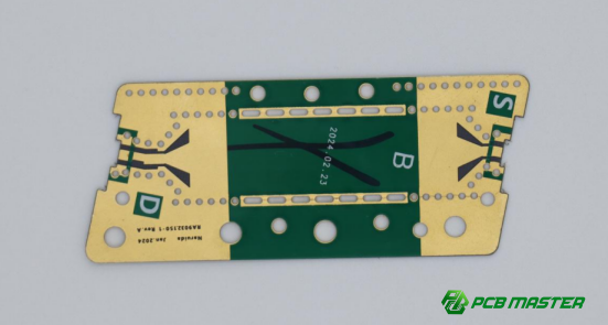
What is Copper Loss at PCB Resin Plug Holes?
Definition and Impact
Copper loss at PCB resin plug holes refers to the problem where the copper layer at the hole's entrance is either partially or completely removed during the manufacturing process. This typically occurs after the resin filling process, where the hole is sealed with resin to prevent the copper from touching the surrounding materials. During subsequent steps like grinding or drilling, the copper layer at the hole’s edge may be scraped off or torn away. This can cause structural weaknesses in the PCB, reducing its mechanical and electrical performance.
The impact of copper loss is significant, as it compromises the integrity of the PCB. Without a complete copper layer at the hole, electrical signals may not travel as intended, leading to circuit failure. The issue also affects the board’s ability to handle mechanical stresses, making it more prone to cracking or breaking during use.
Common Problems and Consequences
Copper loss at the resin plug holes can lead to several critical issues:
1. Reliability: Without the copper layer, the electrical conductivity between different layers of the PCB is compromised, affecting the overall functionality of the circuit. This can result in malfunctioning electronic devices or failure under stress.
2. Production Delays: Detecting and repairing copper loss after the process has been completed can lead to costly delays. If the issue isn’t caught early, the whole batch of PCBs may need to be reworked or scrapped, increasing production time.
3. Increased Costs: Repairing or reworking boards due to copper loss increases production costs. This includes labor, material waste, and possible downtime in manufacturing equipment. Additionally, the board’s reduced quality may lead to higher rates of failure in the final product, requiring additional maintenance or replacements.
What Are the Root Causes of Copper Loss at PCB Resin Plug Holes?
The root causes of copper loss at PCB resin plug holes are the mechanical stress differences between brittle resin and ductile copper, and the structural weakness at the hole's interface where resin, copper, and the base material meet.
The Physical Property Differences Between Resin and Copper
The primary cause of copper loss at PCB resin plug holes lies in the physical differences between the materials involved: resin (often epoxy resin) and copper. Resin is a brittle, non-metallic material, while copper is a ductile, metal with high electrical conductivity. When mechanical stress is applied, such as during the grinding or drilling processes, these materials behave very differently.
Resin, due to its brittle nature, cannot absorb stress as well as copper. It tends to crack or break under force. Copper, on the other hand, can bend or stretch but is still relatively strong. When the resin is applied to seal the hole, it surrounds the copper, but when the resin cracks or pulls away under stress, it can take the copper along with it. This difference in how each material reacts to pressure leads to the copper layer being torn off or damaged, causing the hole to lose copper at the entrance.
Example: In a PCB with a poorly sealed resin plug, mechanical grinding forces might cause the resin to crack, pulling the copper off the hole edge, leading to copper loss.
Weakness at the Hole Structure
The hole in a PCB is a critical structural point where three different materials meet: the resin, the copper layer, and the base material (often fiberglass). This intersection is inherently weak because each material has different properties, particularly in how they expand and contract with changes in temperature.
During processes like soldering or heating, the copper and resin will expand at different rates. This mismatch creates internal stress at the hole's edges. Over time, or under excessive mechanical force, the copper can be pulled away from the resin, leading to copper loss.
Example: If a PCB is heated during the soldering process, the copper and resin will expand differently. As the board cools, the stress at the hole edges can cause the copper layer to crack or detach, particularly at weak points where the copper and resin meet.
In conclusion, the primary causes of copper loss at PCB resin plug holes are the mechanical stress differences between resin and copper, and the structural weakness at the hole's interface. Understanding these root causes is essential for improving the manufacturing process and preventing this common issue.
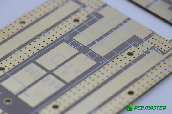
What Are the Specific Problems and Control Points in the PCB Resin Plug Hole Process?
The specific problems in the PCB resin plug hole process include poor drilling quality, weak chemical and electroplated copper layers, incomplete or brittle resin filling, excessive grinding pressure, and poor base material adhesion, with control points focusing on optimizing parameters, improving material selection, and ensuring precise equipment maintenance.
Drilling Process
Problem: Poor Drilling Quality (Rough Hole Walls, Burrs, and Cracks)
Poor drilling quality, such as rough hole walls, burrs, and cracks, can significantly affect the copper plating and resin filling processes. These imperfections create weak points in the PCB that lead to poor adhesion between the copper layer and the resin, increasing the risk of copper loss at the hole. Rough walls also make it harder for subsequent processes to evenly coat the hole with copper, leading to inconsistent plating and reduced mechanical strength.
Solution: Optimize Drilling Parameters, Tool Usage, and Equipment Maintenance
To prevent poor drilling quality, it’s important to optimize drilling parameters such as speed, feed rate, and pressure. Using sharp, high-quality drill bits and maintaining them regularly will ensure cleaner, smoother hole walls. Proper maintenance of drilling equipment and regular inspection can also help reduce the occurrence of cracks or burrs, ensuring a more consistent base for subsequent processes.
Hole Metallization Process
Problem: Poor Chemical Copper Layer (Thin Copper Layer or Weak Adhesion)
A weak or thin chemical copper layer, which serves as the foundation for electroplated copper, can result in poor adhesion and eventual copper loss. This weak layer may not provide the necessary mechanical strength to withstand grinding or stress during further processing.
Problem: Electroplated Copper Layer Quality Issues (Inadequate Thickness)
Insufficient thickness of the electroplated copper layer weakens its mechanical strength and makes it more prone to damage during subsequent processes like grinding. The copper layer must be thick enough to handle stresses without peeling or cracking.
Solution: Strengthen Chemical Copper Control, Optimize Electroplating Process, and Maintain Electroplating Solutions
To address these issues, it is essential to improve the quality control of the chemical copper layer by ensuring proper activation and uniformity. Regular monitoring and maintenance of the electroplating solution are necessary to achieve the required copper thickness and adhesion strength. Fine-tuning the electroplating process, such as adjusting the current and time, can improve the layer’s quality.
Resin Plugging Process
Problem: Incomplete Resin Filling (Air Pockets and Shrinkage Stress)
Incomplete resin filling, often caused by air pockets or uneven resin distribution, creates stress points that can pull the copper off the hole wall. Shrinkage during resin curing can exacerbate these issues, leading to further separation of copper from the hole’s edges.
Problem: Incomplete or Over-Curing of Resin (Weak or Brittle Resin)
If the resin is not fully cured, it will remain weak and prone to cracking. Conversely, over-curing the resin can make it too brittle, causing it to break under stress, which can result in copper damage.
Problem: Mismatch in CTE (Coefficient of Thermal Expansion) Between Resin and Copper
Resin and copper have different thermal expansion rates, which can cause internal stresses when the PCB undergoes temperature changes during processes like soldering. This stress can cause the copper layer to crack or peel off from the resin.
Solution: Optimize Resin Filling Process, Choose Compatible Resin, and Control Curing Process
To prevent these issues, optimizing the resin filling process to ensure complete and bubble-free filling is critical. Selecting resin materials with a CTE (Coefficient of Thermal Expansion) that better matches copper can reduce thermal stress. Strict control over the curing process, including proper temperature ramps and curing times, will ensure the resin has the right strength without becoming too brittle or weak.
Grinding/Polishing Process
Problem: Excessive Grinding Pressure (Direct Impact on Copper Layer)
Excessive grinding pressure can cause the copper layer to peel off or be damaged during the polishing process. The copper layer, especially around the hole, is vulnerable to mechanical stress, and too much pressure will compromise its integrity.
Problem: Coarse or Dull Grinding Paper (Impact on Copper Layer)
Using overly coarse or dull grinding paper can lead to uneven polishing, creating rough surfaces or even tearing the copper. Coarse abrasives tend to apply excessive force, while dull abrasives may not properly smooth the surface, both of which can negatively affect the copper adhesion.
Problem: Warped PCB Surface (Localized Stress Issues)
If the PCB is warped, grinding may lead to uneven pressure, resulting in localized stress and damage to the copper layer around the hole.
Solution: Implement "Two-Step Grinding" or "Multi-Step Grinding" Process, Optimize Grinding Parameters, and Maintain Equipment
To mitigate these issues, a two-step or multi-step grinding process is recommended. In the first step, coarser abrasives are used to remove excess resin, leaving a thin layer over the copper. In the second step, finer abrasives are used to gently smooth the surface, protecting the copper. Optimizing grinding pressure, speed, and abrasive type, along with regular maintenance of grinding equipment, ensures more uniform and gentle polishing.
Material and Design Factors
Problem: Poor Adhesion of Copper to Substrate (Weak Base Material)
The quality of the base material plays a crucial role in the overall copper adhesion. Low-quality substrates, like certain types of PTFE, may have weaker bonding with copper, increasing the likelihood of copper separation during subsequent processes.
Problem: Poor Hole Design (Impact on Copper Stability)
If the hole design places too much stress on the copper layer (e.g., by having sharp edges or improper placement), the copper may become more susceptible to peeling or cracking, especially during temperature changes or mechanical stress.
Solution: Use High-Quality Base Materials and Avoid Sensitive Design Areas
To prevent these issues, selecting higher-quality substrates with better adhesion properties is essential. In addition, careful PCB design should avoid placing holes in areas that are prone to high stress or where copper adhesion could be compromised. Adjusting hole size, shape, and placement can help reduce the risk of copper loss.
How to Effectively Troubleshoot Copper Loss at PCB Resin Plug Holes?
To effectively troubleshoot copper loss at PCB resin plug holes, use microscope or cross-section analysis to locate the issue, check grinding parameters and surface conditions, review electroplating quality through copper thickness and backlight tests, verify resin filling completeness with ultrasonic scanning, and inspect drilling quality for roughness or cracks.
Phenomenon Localization: Microscope or Cross-Section Analysis
To identify the specific cause of copper loss at resin plug holes, the first step is to locate the issue precisely. This can be done using a microscope or cross-sectional analysis. A high-power microscope can reveal the location of copper loss, whether it’s at the hole entrance or deeper within the hole. Cross-sectioning the PCB allows for a detailed view of the internal structure, showing where the copper layer is detached or damaged.
By examining the hole’s edge and surrounding areas, manufacturers can identify if the copper was peeled off during grinding, if there was a problem with the plating, or if the resin failed to fill the hole properly. This focused approach helps pinpoint the problem’s origin, whether in the drilling, plating, resin filling, or grinding process, making the troubleshooting process more efficient.
Grinding Process Check: Focus on Grinding Parameters and Board Surface Condition
The grinding process is a critical step that directly impacts the integrity of the copper layer at the resin plug hole. To check for issues, it’s important to examine the grinding parameters (pressure, speed, abrasive type) and the condition of the PCB surface after grinding. Excessive pressure or inappropriate grinding materials can easily damage the copper layer, while uneven grinding can cause localized stress, leading to copper loss.
By adjusting and optimizing the grinding settings—such as using finer abrasives in later stages or lowering the grinding pressure—manufacturers can avoid excessive damage to the copper layer. Inspecting the surface after grinding helps ensure that the board is smooth and the copper is intact around the hole. Regular monitoring and adjusting these parameters reduce the risk of copper loss during the grinding stage.
Electroplating Quality Review: Testing and Backlight Analysis
Another critical step in troubleshooting is reviewing the quality of the electroplated copper layer. Insufficient copper thickness or poor adhesion can result in copper loss during subsequent processes. To check for plating issues, conduct copper thickness tests and backlight analysis. Copper thickness tests use tools like micrometers to measure if the electroplated copper meets the required specifications (such as IPC-6012 standards).
Backlight analysis involves using a special light to check for inconsistencies in the copper layer, such as thin spots or weak adhesion. If the copper layer appears patchy or detached under backlight, it indicates that the plating process needs improvement. Regular quality control and backlight testing during electroplating can help detect and address copper loss risks before they become more serious issues.
Resin Filling Quality Check: Use Ultrasonic Scanning for Resin Completeness and Quality
Resin filling quality is another crucial factor that can cause copper loss at the hole. Incomplete filling or trapped air pockets can create stress points that pull the copper off the hole. To ensure thorough resin filling, ultrasonic scanning can be used. This non-destructive testing method detects gaps or air pockets within the resin. By applying ultrasonic waves, it’s possible to see how well the resin has filled the hole, and if there are any voids or inconsistencies.
If ultrasonic scanning reveals incomplete filling or air pockets, adjusting the resin filling process (such as improving vacuum pressure or ensuring more uniform resin flow) will be necessary. Ensuring full and consistent resin filling prevents internal stresses and reduces the risk of copper loss.
Drilling Quality Analysis: Inspect Hole Wall Roughness and Cracks
Drilling quality plays a significant role in ensuring copper adhesion to the hole walls. Rough hole walls, burrs, or cracks can reduce the adhesion between the copper and the resin, leading to copper loss during later stages of production. After drilling, it’s essential to inspect the hole wall for roughness or visible cracks. A smooth, clean hole wall improves copper plating adhesion and reduces the likelihood of mechanical stress points that might lead to copper peeling.
To avoid drilling issues, using sharp, high-quality drill bits and optimizing drilling parameters is essential. Routine checks of drilling equipment and maintenance also ensure that holes are properly formed, avoiding cracks or rough walls that could cause copper loss later in the process.
How to Optimize the Resin Plug Hole Process to Prevent Copper Loss?
To optimize the resin plug hole process and prevent copper loss, analyze and improve each production step, implement regular monitoring and quality checks, and establish standardized operating procedures (SOPs) along with comprehensive operator training.
Overall Process Optimization: Analyzing Each Step and Creating Effective Improvement Plans
To prevent copper loss at resin plug holes, it’s important to look at the entire production process and optimize each step. From drilling and plating to resin filling and grinding, every stage can impact the final outcome. By analyzing the entire process, you can identify weak points where copper loss may occur.
For instance, if drilling produces rough hole walls, it could affect copper adhesion during plating. Similarly, improper resin filling or excessive grinding pressure could also lead to copper peeling. A comprehensive improvement plan should include optimizing each step with clear guidelines and tools, ensuring consistency and reducing the risk of copper loss.
Example: By improving the drilling process with sharper tools and better speed control, and by optimizing the resin filling process to ensure complete and bubble-free filling, manufacturers can significantly reduce copper loss at resin plug holes.
Preventive Measures: Regular Monitoring and Quality Inspections to Identify Potential Issues Early
Regular process monitoring and quality checks are key to preventing copper loss. By conducting frequent inspections at each stage of production, manufacturers can catch issues before they escalate into larger problems. This can be achieved by setting up routine checks for drilling quality, copper plating thickness, resin filling, and grinding pressure.
For example, using ultrasonic scanning to check resin filling quality and performing backlight tests for electroplating thickness can help detect issues early. Regular process audits and performance tracking will ensure that any deviation from standards is identified and corrected in time.
Example: In a factory setting, implementing weekly quality control reviews for resin filling and copper plating can identify defects before they result in copper loss, thus saving time and reducing material waste.
Standardized Operating Procedures (SOP) and Training: Establishing Clear Processes and Educating Staff
Standardizing the process through detailed Standard Operating Procedures (SOPs) and training for operators is crucial to avoid variations that lead to copper loss. Clear, step-by-step guidelines should be in place for every process, from drilling to grinding, so operators know exactly how to perform each task correctly.
Training ensures that all staff understand the importance of each step and the impact it has on the overall quality. This helps reduce human errors and improves consistency across the production line. Regular refresher courses and skills testing can help maintain a high level of competence among workers.
Example: By implementing an SOP that outlines precise parameters for drilling speed, copper plating thickness, and grinding pressure, and training operators to follow these standards, a manufacturer can significantly reduce inconsistencies and the risk of copper loss.
Conclusion
Preventing copper loss at PCB resin plug holes is essential for ensuring the reliability and functionality of printed circuit boards. By optimizing each step of the production process, from drilling and plating to resin filling and grinding, manufacturers can minimize defects and improve product quality. Regular monitoring, quality inspections, and standardized procedures further enhance the process, reducing the likelihood of costly errors.
For businesses seeking a trusted partner to handle their PCB and PCBA needs, companies like PCBMASTER provide decades of expertise and commitment to quality. As an experienced supplier, PCBMASTER is dedicated to delivering high-quality products and solutions that meet the highest industry standards, ensuring your projects are built to last.
FAQs
1. What is the copper loss at the resin plug hole, and how is it detected?
Copper loss at the resin plug hole refers to the issue where the copper layer at the entrance of a PCB hole is either missing or cracked due to issues during the manufacturing process. This typically occurs during the resin filling, copper plating, or grinding stages. The lack of copper at the hole’s edge can affect both the electrical conductivity and mechanical strength of the PCB, leading to circuit failures or reliability problems.
How to detect it:
This issue is often detected through microscopic analysis or cross-sectional (slice) analysis of the PCB. By examining the board under a microscope or cutting the PCB to inspect the hole's internal structure, manufacturers can easily spot areas where the copper layer is missing, broken, or improperly adhered. These inspections help pinpoint the exact location of the defect, allowing for corrective actions to be taken at the appropriate stage in the manufacturing process.
2. Why is the copper layer at the hole entrance prone to tearing during the grinding process?
The copper layer at the hole entrance is vulnerable to tearing during grinding due to excessive pressure or the use of improper abrasive materials. During the grinding process, high pressure can cause the copper to detach from the resin and base material, particularly at the hole’s edge, where the copper is thinnest. Additionally, using abrasive materials that are too coarse or worn can either grind too aggressively, causing the copper to strip away, or create uneven surfaces, which result in mechanical stress.
How to prevent this:
To avoid this, it is crucial to optimize grinding parameters, such as reducing the grinding pressure and selecting the appropriate abrasive material. Using a two-step grinding process (first coarse grinding and then fine grinding) ensures that the copper layer remains intact while the resin is smoothed and levelled. Regular checks and maintenance of grinding equipment will also help prevent inconsistent grinding that can lead to copper loss.
3. How to ensure that the electroplated copper layer meets quality requirements?
To ensure that the electroplated copper layer meets the required quality standards, it is important to strictly control electroplating process parameters, such as current density, plating time, and bath chemistry. These factors influence the thickness, uniformity, and adhesion of the copper layer.
Key steps to ensure quality:
l Regular copper thickness testing: Measure the thickness of the copper plating to ensure it meets industry standards (e.g., IPC-6012 Class 2, which requires an average thickness of 20μm).
l Adhesion strength tests: Perform adhesion tests to ensure the copper layer will remain intact under mechanical stresses like grinding or thermal cycling.
l Backlight inspection: Use backlight testing to detect any thin or poorly bonded areas in the copper layer that may be prone to failure.
By maintaining these quality control measures and regularly monitoring the electroplating process, manufacturers can avoid weak or inconsistent copper plating that could lead to copper loss at the hole entrance.
4. How does the difference in CTE (Coefficient of Thermal Expansion) between resin and copper affect the resin plug hole?
CTE (Coefficient of Thermal Expansion) refers to the rate at which materials expand or contract with temperature changes. Copper and resin (usually epoxy resin) have very different thermal expansion properties. Copper has a low CTE, meaning it expands and contracts very little with temperature changes. Resin, on the other hand, has a higher CTE, causing it to expand and contract more during thermal cycles.
How it affects resin plug holes:
l When the PCB is exposed to heat (e.g., during soldering or thermal cycling), the resin and copper will expand and contract at different rates, creating internal stresses at the hole interface.
l This stress can lead to copper layer delamination, where the copper separates from the resin, resulting in copper loss at the hole entrance.
How to address this:
l One solution is to choose resins with thermal expansion properties that are more closely matched to those of copper. This reduces the stress at the resin-copper interface during thermal cycles.
l Additionally, controlling the curing process to ensure the resin is properly solidified can help mitigate CTE mismatch issues.
5. How to optimize the drilling process to avoid copper loss at the hole entrance?
The drilling process is a crucial step in preventing copper loss at the hole entrance. If the hole is not drilled cleanly, it can cause rough hole walls, cracks, or burrs, which reduce copper adhesion during electroplating and resin filling. These issues increase the risk of copper being torn off during subsequent processes like grinding.
Steps to optimize the drilling process:
1. Use sharp drill bits: Ensure the drill bits are sharp and in good condition to produce clean, smooth hole walls. Dull bits can cause roughness and cracks, making it difficult for copper and resin to adhere properly.
2. Optimize drilling parameters: Adjust parameters like drilling speed, feed rate, and pressure to achieve smoother holes. Too high of a speed or pressure can cause thermal damage or create micro-cracks in the hole.
3. Regular equipment maintenance: Keep the drilling equipment well-maintained and inspect it regularly to avoid inconsistencies or defects during the drilling process.
4. Smooth hole walls: After drilling, inspect the hole walls for roughness and any visible cracks or burrs. If necessary, perform additional cleaning or deburring steps to ensure the walls are smooth and ready for plating and resin filling.
By optimizing the drilling process, manufacturers can ensure a better surface for copper plating and resin filling, reducing the likelihood of copper loss during later production stages.

