


PCIe PCB Design Guide: Signal Integrity and Layout Best Practices
Modern computers rely on PCIe to connect high-speed components like graphics cards and NVMe SSDs. Designing a PCB to handle these speeds can be tricky: signal integrity, layout, and material choices all affect performance. Beginners often struggle to know where to start or what matters most.
To make this easier, PCBMASTER shares its experience in high-speed PCB and PCBA design. In this guide, we explain the fundamentals of PCIe, from how lanes carry data to how layout impacts bandwidth, along with practical tips for maintaining signal quality. By understanding these essentials, even first-time designers can create reliable, high-performance PCIe boards with confidence.
Let’s start!
What is a PCIe Interface and What Role Does It Play in Modern Computers?
PCIe is a high-speed interface standard that connects critical components inside modern computers, enabling fast data transfer and high performance. It replaces older PCI connections and is essential for gaming, storage, networking, and industrial applications.
PCIe Interface Overview
PCIe, or Peripheral Component Interconnect Express, is a high-speed serial bus standard used to connect devices to a computer’s motherboard. Unlike older parallel PCI slots, PCIe transmits data serially, which allows faster speeds and more efficient communication.
l Key Advantages: PCIe offers high bandwidth, low latency, and flexible lane configurations. It can scale from one lane (x1) to sixteen lanes (x16) depending on the device’s needs.
l Comparison with Traditional PCI: Traditional PCI uses parallel communication, which is slower and less efficient for modern applications. PCIe lanes can transmit data simultaneously, making it ideal for graphics cards, SSDs, and networking equipment.
Example: A modern graphics card using PCIe x16 can transfer several gigabytes of data per second, far exceeding what older PCI slots could handle.
This design makes PCIe a core standard in computing, especially for high-speed components where performance matters most.
Applications of PCIe Interfaces
PCIe interfaces are widely used in computing devices to connect high-speed components that require fast and reliable data transfer.
l High-Performance Graphics Cards: Gaming and workstation GPUs rely on PCIe x16 lanes for maximum data throughput to render complex graphics quickly.
l NVMe Solid-State Drives: PCIe provides the high-speed lanes required for NVMe SSDs, reducing storage latency and speeding up file access.
l High-Speed Network Cards & Server Expansion: Data center servers use PCIe network cards for 10G, 25G, or higher network speeds. PCIe slots allow easy server upgrades without changing the motherboard.
l Industrial and Embedded Systems: In robotics, medical devices, and automation systems, PCIe connects specialized modules, enabling fast sensor data processing and control.
Example: In a data center, a PCIe-based NVMe RAID storage system can handle thousands of read/write operations per second, supporting high-traffic cloud applications.
How Do PCIe Transmission Speed and Lane Design Affect PCB Layout?
PCIe transmission speed and lane configuration directly determine how a PCB must be designed. High-speed lanes require precise layout, controlled impedance, and careful signal management to achieve optimal performance.
PCIe Lanes (Lane) and Bandwidth Basics
PCIe lanes are the channels through which data travels. The number of lanes affects both the physical slot size and data bandwidth.
l Lane Configurations: PCIe slots come in different sizes: x1 (1 lane), x4 (4 lanes), x8 (8 lanes), and x16 (16 lanes). The physical length of the slot corresponds to the number of lanes it supports. More lanes allow higher total data throughput.
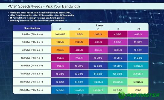
l Bandwidth Calculation:
Single-direction bandwidth = Transfer Rate × Encoding Efficiency × Number of Lanes
Bi-directional bandwidth = Single-direction bandwidth × 2
l Protocol Overhead: The effective bandwidth is slightly less than theoretical bandwidth due to protocol overhead, usually 97%–98% of the theoretical value.
Example: A PCIe Gen4 x16 slot can theoretically transfer up to 32 GB/s in total, but effective data throughput is slightly lower after accounting for protocol overhead.
Understanding GT/s (GigaTransfers per Second)
GT/s measures how many data transfers happen per second per lane. It helps compare PCIe generations and their performance.
l Concept: 1 GT/s means one billion data transfers per second.
l PCIe Generation Speeds:
| PCIe Generation | Transfer Rate (GT/s) |
| Gen3 | 8 GT/s |
| Gen4 | 16 GT/s |
| Gen5 | 32 GT/s |
| Gen6 | 64 GT/s |
| Gen7 | 128 GT/s |
l Practical Meaning: Higher GT/s allows more data to pass through each lane in a given time, but it also increases the design challenge for PCB layout, signal integrity, and crosstalk management.
Example: Upgrading from Gen3 to Gen5 doubles the lane speed, requiring tighter impedance control and shorter trace lengths on the PCB.
How PCB Design Affects Bandwidth Optimization
PCB layout directly impacts PCIe performance. Proper lane matching and signal routing are critical to maintain bandwidth and signal quality.
l Differential Pair Matching: Each lane uses a differential pair. Matching trace width, spacing, and impedance ensures minimal signal reflection and loss.
l Signal Loss & Crosstalk: Longer traces, sharp corners, or improper spacing can introduce signal loss and interference between lanes. Using careful trace routing, spacing rules, and avoiding unnecessary vias helps reduce these issues.
l Practical Tip: Designers often prioritize shorter, straighter routes with smooth curves, controlled impedance, and minimal layer transitions to maintain bandwidth.
Example: A Gen4 x8 PCIe layout might limit trace lengths to under 12 inches and use precise differential impedance control to ensure signals reach the GPU or NVMe drive without errors.
How to Achieve PCIe Signal Integrity (SI) Optimization in PCB Design?
Signal integrity (SI) ensures that PCIe signals travel accurately across the PCB without distortion or loss. Proper impedance control, trace design, loss management, and crosstalk reduction are key to maintaining high-speed signal quality.
Impedance Control and Trace Design
Controlling impedance is essential for PCIe signal integrity. Each differential pair should have a target impedance of 100Ω ±10% (or 50Ω for single-ended signals).
l Board Material (Dk) Impact: The dielectric constant (Dk) of the PCB material affects impedance. A consistent Dk ensures that signal speed and reflection remain stable. For example, materials like Megtron or Tachyon offer predictable Dk for high-speed designs.
l Impedance Discontinuities: Points where the impedance changes, such as vias, connectors, or layer transitions, can cause reflections. Optimizing via size, using back-drilling to remove stubs, and designing connector pads carefully helps minimize these effects.
Example: In a PCIe Gen5 x8 layout, controlling impedance within ±5% reduces errors and allows reliable data transfer at 32 GT/s per lane.
Loss Management and Trace Length Control
Signal loss increases with trace length and frequency. Managing trace lengths and choosing low-loss materials are critical for PCIe performance.
l Maximum Trace Lengths: Each PCIe generation has recommended maximum trace lengths. For example, Gen3/4 traces should not exceed ~20 inches, while Gen5/6 traces are limited to ~12 inches.
l Material Selection: High-frequency losses are reduced with ultra-low-loss PCB materials (Df ≤ 0.002), which maintain signal integrity over longer distances.
Example: Using a Megtron6 board for a Gen4 PCIe x16 slot ensures minimal insertion loss and reliable communication over a standard motherboard layout.
Crosstalk Suppression and Trace Spacing Guidelines
Crosstalk occurs when adjacent signal traces interfere with each other, causing errors. Proper spacing and layout reduce this effect.
l 3W Rule: Keep the center-to-center distance between differential pairs at least three times the trace width (e.g., 5 mil width → 15 mil spacing).
l High-Speed Layout Practices: Avoid sharp 90° turns, use smooth arcs or 45° bends, maintain consistent spacing, and route critical PCIe signals on inner layers with controlled reference planes.
Example: A Gen5 x8 PCIe design may route differential pairs with 10 mil width and 30 mil spacing, using controlled impedance layers and avoiding parallel traces to sensitive signals, keeping crosstalk below -40 dB.
What Are the Key Considerations for High-Speed PCIe PCB Design?
High-speed PCIe PCB design requires careful attention to via and connector design, trace routing, and material selection. These factors ensure signal integrity, minimize loss, and maintain reliable high-speed communication.
Via and Edge Connector (Gold Finger) Design Requirements
Proper via and gold finger design is critical to prevent signal reflections and maintain consistent impedance in high-speed PCIe designs.
l Via Limits: For Gen3/4 designs, limit to two pairs of vias per lane; for Gen5/6, use no more than one pair to reduce signal distortion.
l Back Drilling: Unused via stubs can reflect signals and degrade performance. Back drilling removes these stubs, improving signal quality at higher PCIe generations.
l Anti-Pad Precision: The pad around the via (anti-pad) must be accurately sized to maintain differential impedance and prevent discontinuities.
Example: In a Gen5 x8 PCIe layout, back-drilling vias and carefully controlling anti-pad dimensions can reduce reflections, keeping insertion loss within acceptable limits for 32 GT/s lane speeds.
Serpentine Traces and Corner Optimization
Trace routing affects timing and signal quality. Proper serpentine patterns and corner design prevent mismatch and reflections.
l Serpentine Trace Curvature: The arc radius should be at least three times the trace width. This avoids sharp bends that can distort signals.
l Corner Routing: Avoid 90° corners. Use 45° or rounded bends to maintain smooth current flow and minimize reflections.
Example: A PCIe Gen6 differential pair routed with 6 mil width traces uses serpentine arcs of 18 mils radius and 45° turns to match signal length while maintaining integrity.
PCB Material Selection Strategies
The choice of PCB material directly impacts signal loss and achievable bandwidth for PCIe.
| PCIe Generation | Recommended PCB Material | Key Notes / Advantages |
| Gen1–3 | Standard FR4 (e.g., Isola 370HR) | Sufficient for lower-speed designs; cost-effective and widely available. |
| Gen4+ | Ultra-low-loss materials (Megtron6, Tachyon 100G) | Reduce high-frequency attenuation; maintain clean signals; suitable for faster lanes. |
| PCIe 5.0/6.0/7.0 | Ultra-low-loss materials with Df ≤ 0.0015–0.001 | Tighter dielectric constant control; supports extremely high-speed signals; required for next-gen PCIe. |
Example: Upgrading from a Gen3 NVMe slot to a Gen5 design on the same PCB requires replacing FR4 with Megtron6 to prevent excessive insertion loss and ensure reliable data transfer at 32 GT/s.
How to Verify and Test PCIe PCB Design Performance?
Verifying PCIe PCB design ensures that signals travel accurately, loss is minimized, and the board performs reliably at high speeds. Key testing methods include insertion/return loss measurements, crosstalk testing, and TDR verification.
Insertion and Return Loss (S-Parameter) Testing
S-parameters measure how much signal is transmitted and reflected through PCIe lanes. This testing identifies potential design flaws and optimizes performance.
l Insertion Loss: Represents signal attenuation as it travels along the PCB. For Gen4 designs, insertion loss should be ≤ -8 dB at 8 GHz to ensure sufficient signal strength.
l Return Loss: Measures reflected signals caused by impedance mismatches. High return loss indicates good impedance control.
l Optimization Use: Engineers use S-parameter data to adjust trace widths, via sizes, or connector layouts for better signal quality.
Example: A Gen4 x8 PCIe board with measured insertion loss of -7 dB at 8 GHz may require slight impedance tuning to reduce reflection and ensure error-free data transfer.
Crosstalk Testing Standards
Crosstalk occurs when signals from adjacent traces interfere, creating errors. Testing ensures interference stays within acceptable limits.
l Crosstalk Limit: High-speed PCIe designs typically require crosstalk ≤ -40 dB between adjacent lanes.
l Feedback Process: Test results inform design adjustments, such as increasing trace spacing, adding ground shields, or rerouting critical signals to reduce interference.
Example: A Gen5 PCIe board shows -38 dB crosstalk on some lanes; engineers increase spacing and adjust reference planes, reducing interference below -40 dB.
TDR (Time Domain Reflectometry) Measurement
TDR measures impedance along the PCB traces to detect discontinuities or mismatches that can cause reflections.
l Impedance Verification: Ensures differential pairs maintain consistent impedance, typically around 100Ω ±5Ω.
l Waveform Analysis: TDR identifies short sections with spikes or dips in impedance, indicating problem areas such as vias or connector pads.
l Design Refinement: Engineers can adjust trace width, spacing, or layer stacking based on TDR results to achieve smooth, continuous impedance.
Example: Using TDR on a Gen6 PCIe x16 board, an impedance spike at a via is detected. Back-drilling and pad resizing corrects it, keeping the trace within ±5Ω of the target.
What Are Advanced PCB Design Strategies for PCIe 5.0/6.0 and Future Gen7?
High-speed PCIe designs at Gen5, Gen6, and future Gen7 require advanced materials, precise impedance control, and rigorous high-frequency testing to ensure reliable performance at extreme data rates.
Ultra-Low-Loss Materials and High-Frequency Optimization
Using ultra-low-loss PCB materials is essential to minimize signal attenuation at high PCIe frequencies.
l Material Df ≤ 0.0015: The dissipation factor (Df) measures how much signal energy is lost as heat. Materials like Megtron8 or Tachyon 200G with Df ≤ 0.0015 maintain signal integrity for Gen5/6 designs.
l Laser Blind Via and Filled Via Technology: Laser-drilled blind vias, combined with plating fill, reduce stub length and minimize reflections at high frequencies, allowing clean signals at tens of GHz.
Example: A Gen6 x16 PCIe board using Megtron8 and laser blind vias maintains low insertion loss, supporting reliable 32 GT/s per lane communication.
Improved Impedance and Via Accuracy
Maintaining precise impedance and via dimensions is critical for ultra-high-speed PCIe.
l Impedance Tolerance: Differential pairs should stay within 100Ω ±3% to prevent reflections and maintain signal quality.
l Back-Drilling and Stub Removal: Residual via stubs must be ≤25 μm. Precision back-drilling and post-processing ensure minimal impedance discontinuity.
Example: On a Gen7 PCIe design, controlling impedance tightly and reducing via stubs allows signal transmission above 64 GT/s without errors.
High-Frequency Signal Testing Requirements
Testing at extreme frequencies ensures the board can handle future Gen7 data rates reliably.
l Insertion Loss and Crosstalk ≥ 28 GHz: High-frequency PCIe testing verifies that insertion loss and crosstalk stay within acceptable limits. This ensures data integrity at multi-GT/s speeds.
l Laser Direct Imaging (LDI) Process: LDI provides high-resolution PCB patterning for precise trace widths, spacing, and impedance control. It supports ultra-high-speed designs by reducing manufacturing variation.
Example: A Gen7 x16 PCIe PCB tested at 28 GHz with LDI-manufactured traces shows minimal insertion loss and crosstalk below -36 dB, meeting next-generation speed requirements.
Conclusion
Designing high-speed PCIe PCBs is a careful balance of material choice, trace layout, impedance control, and rigorous testing. Each detail—from lane configuration to via precision—directly affects signal quality and overall system performance. By understanding the fundamentals and advanced strategies for Gen3 through Gen7 designs, engineers can create boards that deliver reliable, high-bandwidth connections for GPUs, NVMe drives, and server expansions.
PCBMASTER, with years of experience in high-speed PCB and PCBA design, has helped countless projects navigate these challenges. Whether it’s selecting ultra-low-loss materials, optimizing differential pair routing, or verifying high-frequency performance, our expertise ensures that each design meets both technical requirements and real-world application needs.
With careful planning and the right guidance, even complex PCIe layouts become manageable, allowing designers to confidently push the limits of performance. PCBMASTER continues to share practical insights, helping engineers turn advanced high-speed designs into functional, reliable PCBs that excel in modern computing systems.
FAQs
1. What are the trace length limitations for different PCIe generations?
Trace lengths depend on PCIe generation to maintain signal integrity. Gen3 and Gen4 traces should not exceed ~20 inches, while Gen5 and Gen6 are limited to ~12 inches. Shorter traces reduce signal loss and reflections, ensuring reliable high-speed data transmission.
2. Why is differential impedance accuracy critical for PCIe signal stability?
Differential impedance controls how signals travel along paired traces. Accurate impedance (typically 100Ω ±10% for most designs, ±3% for Gen5/6) minimizes reflections and distortion. Deviations can cause errors, reduce effective bandwidth, and compromise PCIe performance.
3. How can crosstalk be effectively suppressed in PCB design?
Crosstalk is reduced by proper trace spacing, controlled routing, and shielding. The 3W rule—keeping the spacing between differential pairs at least three times the trace width—is widely applied. Rounded or 45° turns and careful layer stacking also help minimize interference between high-speed signals.
4. What advantages do ultra-low-loss PCB materials offer in high-speed PCIe design?
Ultra-low-loss materials (Df ≤ 0.0015) reduce signal attenuation and maintain integrity over long or high-frequency traces. They allow higher GT/s speeds, lower insertion loss, and more reliable communication for Gen5, Gen6, and future Gen7 PCIe designs.
5. How are back-drilling and blind via techniques applied in PCIe PCBs?
Blind vias connect inner layers without passing through the entire board, reducing stub length. Back-drilling removes residual via stubs to prevent signal reflections. These techniques improve impedance continuity and enable clean high-speed PCIe signals in multi-layer boards.

