


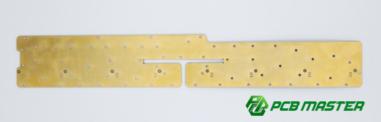
What Is a PCB Via? Types, Functions, and Design Guidelines
Modern electronic devices continue to become smaller, faster, and more functionally complex, placing greater demands on PCB design. While components and traces often receive most of the attention, one critical feature works quietly behind the scenes to make multilayer circuit boards possible: the PCB via.
These tiny conductive pathways do far more than connect different layers of a board. They influence routing efficiency, signal performance, thermal management, manufacturing complexity, and even the overall reliability of the finished product. As designs evolve toward higher densities and faster data rates, understanding how vias are used has become increasingly important for both PCB designers and electronics manufacturers.
Whether you're selecting a suitable via structure for a new project or refining an existing layout, knowing the strengths, limitations, and design considerations of different via types can help you make more informed decisions. The following guide explores what PCB vias are, the main types used in modern PCB design, the functions they perform, and the key guidelines that contribute to better-performing and more manufacturable circuit boards.
What Is a PCB Via?
A PCB via is a small plated hole that creates an electrical connection between different layers of a printed circuit board (PCB). It allows signals, power, and ground connections to travel through a multilayer board, making modern electronic designs more compact and efficient.
Definition of a PCB Via
A PCB via is a conductive hole drilled through one or more layers of a printed circuit board to connect copper traces on different layers. Unlike component holes, vias are typically not used to mount electronic parts. Their primary purpose is to provide an electrical pathway inside the board.
Think of a PCB as a multi-story building. Copper traces are like hallways on each floor, while vias act as elevators that allow electrical signals to move from one floor to another. Without vias, designers would be limited to routing connections on a single layer, making complex circuits much larger and less practical.
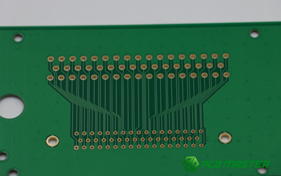
Because of this role, PCB vias are a fundamental feature in multilayer PCB design. They help increase routing density, support compact layouts, and enable the advanced functionality required in products such as smartphones, laptops, automotive electronics, and industrial control systems.
Key takeaway: A PCB via is a plated interconnection that enables electrical communication between PCB layers.
How a PCB Via Works in a Multilayer PCB
A PCB via works by forming a conductive path through the board, allowing electricity to move between copper layers that cannot be connected directly on the same surface.
In a multilayer PCB, each copper layer has a specific purpose. Some layers carry signals, while others distribute power or serve as ground planes. When a trace needs to continue onto another layer, a via provides the transition point.
The process is straightforward:
· A hole is drilled through the PCB during manufacturing.
· The inner wall of the hole is coated with copper through plating.
· The plated hole connects the copper pads attached to the required layers.
· Electrical current can then travel through the via to reach another layer.
For example, imagine a signal trace on the top layer of a four-layer PCB that needs to bypass other routing paths. Instead of crossing over existing traces, the signal enters a via, travels through the plated barrel, and continues on an inner or bottom layer. This approach improves routing flexibility and saves valuable board space.
Key takeaway: A PCB via functions as a vertical electrical bridge that links different copper layers within a multilayer PCB.
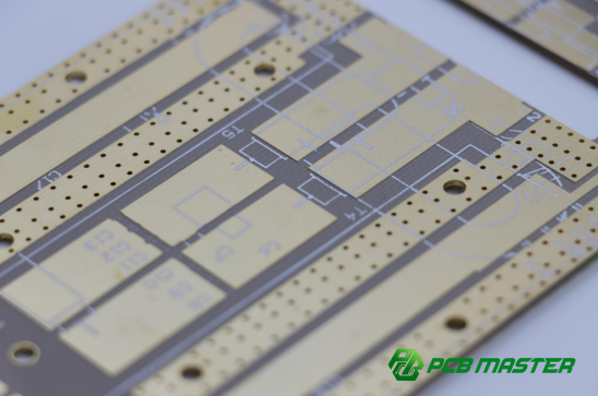
The Basic Structure of a PCB Via
A standard PCB via consists of three main elements: the barrel, the pad, and the antipad. Each part serves a specific purpose in ensuring reliable electrical performance and manufacturability.
Barrel
The barrel is the conductive wall inside the drilled hole. It is created by depositing copper onto the hole surface during the plating process.
Its main function is to carry electrical current between connected layers. The quality and thickness of the copper plating directly affect the via's reliability, especially in applications involving high current or repeated temperature changes.
A simple way to understand the barrel is to think of it as the metal lining inside a tunnel. It forms the actual pathway that electricity travels through.
Key point: The barrel is the conductive channel that makes layer-to-layer electrical connection possible.
Pad
The pad is the circular copper area surrounding the via opening on a PCB layer. It connects the via barrel to the copper trace on that layer.
Pads provide enough copper area to ensure a secure electrical connection and support manufacturing tolerances during drilling. If the pad is too small, slight drill misalignment may weaken the connection or lead to defects.
For example, when a signal trace reaches a via, it first joins the pad before entering the barrel and continuing to another layer.
Key point: The pad links the via to the PCB trace and helps maintain a reliable connection.
Antipad
The antipad is a clearance area around the via in copper layers that are not intended to be electrically connected.
Although it may seem like empty space, the antipad plays an important role. It prevents accidental contact between the via and nearby copper planes, reducing the risk of short circuits and unwanted electrical effects.
For instance, if a signal via passes through a ground plane without needing a connection, an antipad creates an insulating gap around the via at that layer.
You can think of the antipad as a safety zone that keeps unrelated circuits separated.
Key point: The antipad isolates the via from non-connected copper layers to maintain proper electrical performance.
Structure of a PCB Via at a Glance
| Via Element | Primary Function | Simple Explanation |
| Barrel | Conducts electricity between layers | The tunnel electricity travels through |
| Pad | Connects the via to PCB traces | The entry and exit point of the tunnel |
| Antipad | Prevents unwanted connections | The protective space around the tunnel |
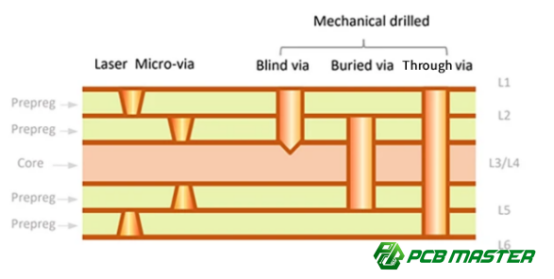
Understanding these three elements provides a solid foundation for learning how different PCB via types, such as through-hole vias, blind vias, buried vias, and microvias, are designed and used in modern circuit boards.
What Are the Main Types of PCB Vias?
The main types of PCB vias (printed circuit board vias) are through-hole vias, blind vias, buried vias, and microvias. Each type is used to connect different PCB layers depending on design density, signal speed, and manufacturing requirements.
Through-hole vias
Through-hole vias are the most common type of PCB via. They pass completely through the PCB, connecting the top layer to the bottom layer and sometimes all internal layers.
Features
Through-hole vias are drilled straight through the entire board structure and plated with copper to create an electrical connection across all layers. They are easy to manufacture and highly reliable, which makes them widely used in general PCB via design and standard multilayer PCB manufacturing.
A key feature is their full-stack connectivity, meaning one via can connect every layer if needed. However, this also creates longer via stubs, which can slightly affect high-speed signal performance.
Key point: Through-hole vias are simple, strong, and cost-effective but less ideal for very high-speed PCB design.
Typical applications
Through-hole vias are commonly used in low to medium-speed PCB designs, such as power supplies, consumer electronics, and industrial control boards.
For example, in a basic LED driver board, a through-hole via may connect a power trace on the top layer to a ground plane on the bottom layer. Their simplicity makes them ideal for general PCB routing via connections where signal integrity is not highly sensitive.
Blind vias
Blind vias connect an outer layer (top or bottom) to one or more inner layers but do not pass through the entire PCB.
Features
Blind vias are drilled from one side of the PCB and stop at a specific inner layer. This partial-depth structure helps save space and improves routing density in compact PCB designs.
They are commonly used in HDI PCB via design because they reduce unused via length and help improve signal performance by minimizing via stubs.
However, blind vias are more complex to manufacture because they require controlled depth drilling or laser drilling.
Key point: Blind vias improve routing efficiency and are widely used in compact, high-density PCB designs.
Typical applications
Blind vias are often used in smartphones, tablets, and compact IoT devices, where space is limited.
For example, in a smartphone mainboard, a blind via may connect the surface-mounted processor to an internal signal layer without occupying space on all layers. This helps designers achieve high-density interconnect (HDI) routing.
Buried vias
Buried vias connect only internal layers of a PCB and are completely hidden from the outer surfaces.
Features
Buried vias are formed between inner layers before the outer layers are laminated. They do not appear on the top or bottom surface of the PCB.
This structure allows designers to route signals inside the board without consuming surface routing space. It is especially useful in complex multilayer PCB via stack-ups.
However, buried vias increase manufacturing steps and cost because they require sequential lamination processes.
Key point: Buried vias are fully internal connections used to maximize surface routing space.
Typical applications
Buried vias are used in advanced multilayer PCBs, such as telecommunications equipment and high-performance computing boards.
For example, in a router motherboard, buried vias may connect internal ground and signal layers while leaving outer layers free for high-speed routing and component placement.
Microvias
Microvias are very small laser-drilled vias used in HDI (High-Density Interconnect) PCBs to connect adjacent layers only.
Features
Microvias are typically less than 150 microns in diameter and are created using laser drilling instead of mechanical drilling.
They usually connect only one layer to the next (known as single-level microvias). In some advanced designs, stacked or staggered microvias are used for deeper connections.
Because of their small size, microvias reduce parasitic inductance and improve high-speed signal performance in PCB via design.
Key point: Microvias are ultra-small vias designed for high-speed and high-density PCB applications.
Typical applications in HDI PCBs
Microvias are widely used in HDI PCBs for smartphones, wearable devices, and high-speed processors.
For example, in a modern smartphone CPU package, microvias connect the processor directly to inner routing layers with minimal signal delay, improving performance for high-frequency data transfer.
PCB via types comparison
Different PCB via types vary in routing flexibility, cost, and manufacturing complexity. The selection depends on design density, signal speed, and budget constraints.
Routing capability
Through-hole vias provide full-layer connectivity but occupy more space. Blind vias and microvias improve routing flexibility by freeing inner and outer layers. Buried vias maximize surface routing efficiency by staying inside the board.
Key point: Smaller and partial vias improve routing density in compact PCB designs.
Cost
Through-hole vias are the most cost-effective. Blind and buried vias increase cost due to additional manufacturing steps. Microvias are also more expensive because of laser drilling and HDI processes.
Key point: Higher routing density usually increases PCB manufacturing cost.
Manufacturing complexity
Through-hole vias are simple to manufacture using standard drilling. Blind and buried vias require sequential lamination. Microvias require precision laser drilling and strict process control.
Key point: The more advanced the via type, the higher the manufacturing complexity.
Comparison table
| Via Type | Connection Range | Routing Efficiency | Cost Level | Manufacturing Complexity | Typical Use Case |
| Through-hole | Top to bottom (all layers) | Medium | Low | Low | Power boards, general electronics |
| Blind via | Outer to inner layers | High | Medium | Medium-High | Smartphones, compact PCBs |
| Buried via | Inner layers only | High | High | High | Multilayer telecom and computing boards |
| Microvia | Adjacent layers only | Very High | High | Very High | HDI PCBs, high-speed devices |
This classification helps engineers choose the right PCB via type based on performance requirements, board space limitations, and manufacturing budget.
What Functions Do PCB Vias Perform?
PCB vias perform four main functions in circuit board design: signal transmission, power and ground distribution, thermal heat dissipation, and EMI control through stitching connections. Each function supports electrical performance, stability, and reliability in multilayer PCB designs.
Signal transmission vias
Signal transmission vias are used to carry electrical signals between different layers of a PCB, allowing traces to change layers without losing connectivity.
Signal vias are a core part of PCB via routing design, especially in multilayer boards where signals cannot stay on a single layer. When a trace needs to avoid congestion or cross other traces, a via provides a vertical path through the board.
For example, in a high-speed PCB signal routing via scenario, a signal from a processor on the top layer may need to reach memory on an inner layer. The signal enters the via, travels through the plated barrel, and continues on another layer.
In high-speed designs, signal vias must be carefully optimized because every via adds parasitic inductance and capacitance, which can affect signal integrity. That is why designers often minimize via count or use microvias in HDI PCB designs.
Key point: Signal vias enable layer switching for electrical signals while balancing routing flexibility and signal quality.
Power and ground vias
Power and ground vias distribute electrical power and provide stable ground connections across multiple PCB layers.
Power and ground vias are essential for maintaining stable voltage delivery in PCB power distribution networks (PDN). They connect power planes and ground planes across different layers, ensuring consistent current flow throughout the board.
For example, in a PCB power via design for a microcontroller board, multiple vias are often placed in parallel to deliver higher current safely. This reduces resistance and prevents overheating.
Ground vias also play a key role in providing a low-impedance return path for signals. Without proper ground via placement, signals may suffer from noise, voltage drops, or unstable performance.
Key point: Power and ground vias ensure stable current delivery and strong reference grounding across multilayer PCBs.
Thermal vias for heat dissipation
Thermal vias transfer heat away from hot components by conducting heat through copper-plated holes into inner or bottom layers of the PCB.
Thermal vias are widely used in PCB thermal management design, especially for high-power components such as LEDs, power ICs, and voltage regulators. They help reduce component temperature and improve long-term reliability.
A typical thermal via structure is placed under a heat-generating component pad. Heat flows from the component into the via barrel and spreads into internal copper planes or a ground plane acting as a heat sink.
For example, in an LED lighting PCB design, multiple thermal vias are placed under the LED pad to quickly transfer heat to the bottom copper layer. This prevents overheating and extends LED lifespan.
Key point: Thermal vias improve heat dissipation by moving heat from hot components into larger copper areas.
Stitching vias for grounding and EMI control
Stitching vias are used to connect ground planes across different layers to improve grounding performance and reduce electromagnetic interference (EMI).
Stitching vias are a key part of PCB EMI suppression design. They create multiple low-impedance connections between ground planes, forming a stable reference ground across the board.
In practical design, stitching vias are often placed along board edges or near high-speed signal paths. This helps reduce electromagnetic radiation and prevents external noise from affecting sensitive circuits.
For example, in a high-speed digital PCB with USB or RF circuits, ground stitching vias are placed around signal lines to create a shielding effect. This improves signal integrity and reduces crosstalk.
Stitching vias are also used in ground pour regions to maintain uniform grounding across multilayer structures.
Key point: Stitching vias enhance EMI performance by strengthening ground continuity and reducing noise interference.
How Do PCB Vias Affect PCB Performance?
PCB vias affect overall PCB performance by influencing routing flexibility, signal integrity, thermal behavior, and long-term reliability. While they enable multilayer design, they also introduce electrical and mechanical trade-offs that must be carefully managed in PCB via design.
Impact on routing flexibility and board density
PCB vias improve routing flexibility and increase board density by allowing traces to move between layers, but excessive via use can reduce available space and complicate layout optimization.
PCB vias are essential for multilayer PCB routing optimization. They allow designers to escape tight routing areas by switching layers instead of forcing all traces to stay on one surface. This significantly increases routing freedom, especially in compact designs like smartphones or IoT devices.
For example, in a high-density PCB layout design, a single via can redirect a congested signal path from the top layer to an inner layer, freeing space for additional components or traces. Without vias, the board would require larger physical size to fit all routing paths.
However, every via also consumes space and introduces a “routing blockage area,” which can limit trace placement around it. Too many vias in a small region can reduce board efficiency.
Key point: PCB vias increase routing flexibility but must be optimized to avoid unnecessary space consumption in high-density designs.
Effects on signal integrity
PCB vias affect signal integrity by introducing electrical discontinuities such as via stubs, parasitic inductance and capacitance, and return path interruptions that can degrade high-speed signals.
Via stubs
Via stubs are unused portions of a via that extend beyond the active signal path. In high-speed PCB via design, these stubs can reflect signals back, causing distortion and signal loss.
For example, in a high-speed DDR memory layout, an unused via stub can create signal reflections that reduce data reliability. Designers often use back-drilling to remove long stubs and improve performance.
Key point: Via stubs increase signal reflection risk in high-frequency circuits.
Inductance and capacitance
Every PCB via introduces parasitic inductance and capacitance because it acts like a small vertical transmission path. In PCB signal integrity design, this can slow down signal edges or distort fast digital signals.
For instance, in RF or GHz-level circuits, even a single via can slightly alter impedance, affecting signal timing and waveform quality. This is why microvias are often preferred in HDI designs—they reduce parasitic effects due to their smaller size.
Key point: Vias add parasitic electrical effects that become critical in high-speed and RF PCB designs.
Return path continuity
Signal return paths must remain continuous to avoid noise and interference. A via can disrupt the return current path if it crosses plane splits or lacks a nearby ground via.
In a PCB ground return path design, if a signal switches layers through a via but the ground reference is not properly connected, the signal may pick up noise or cause EMI issues.
A common solution is placing a nearby ground via to maintain a short return loop.
Key point: Poor return path design around vias increases noise and reduces signal stability.
Thermal and reliability considerations
PCB vias affect thermal performance and reliability by influencing heat flow, mechanical stress distribution, and long-term durability under temperature changes.
Thermally, vias act as vertical heat channels in PCB thermal via design, helping transfer heat from components to copper planes. This improves cooling efficiency, especially for power components like voltage regulators or LED drivers.
For example, in a power PCB design, multiple thermal vias placed under a MOSFET help spread heat into internal ground planes, reducing hotspot formation.
From a reliability perspective, vias are exposed to thermal cycling stress. Repeated heating and cooling can cause copper fatigue inside the via barrel, potentially leading to cracks or failures over time.
Designers often improve reliability by optimizing via size, copper plating thickness, and avoiding excessive thermal stress concentration.
Key point: PCB vias improve heat dissipation but must be designed carefully to avoid long-term mechanical fatigue and reliability issues.
What Are the Key PCB Via Design Guidelines?
Key PCB via design guidelines include selecting the correct via type, defining proper hole and pad sizes, maintaining safe spacing, minimizing unnecessary vias, accounting for high-speed performance, and following manufacturer DFM (Design for Manufacturability) rules. These steps ensure reliable, cost-effective, and high-performance PCB via design.
Choose the right via type for the application
The correct PCB via type should be selected based on electrical requirements, board density, cost, and signal speed.
Different PCB via types (through-hole, blind via, buried via, microvia) serve different design needs. Choosing the wrong type can lead to poor performance or higher cost.
For example, a through-hole via PCB design is suitable for low-cost power boards, while microvias in HDI PCB design are better for smartphones and high-speed processors. Blind and buried vias are often used when routing space is limited in multilayer designs.
A simple selection rule:
· Low cost → Through-hole vias
· Compact design → Blind or microvias
· High layer complexity → Buried vias
Key point: Matching via type to application improves performance and avoids unnecessary manufacturing cost.
Define proper hole and pad sizes
Proper via hole and pad sizes ensure reliable electrical connection and stable PCB manufacturing yield.
In PCB via size design, the hole must be large enough for drilling accuracy, while the pad must be wide enough to tolerate manufacturing tolerances.
For example, if a via hole is too small, it may be difficult to plate properly, leading to weak connections. If the pad is too small, drill misalignment may cause open circuits.
A common industry practice is to maintain a balanced ratio between drill size and pad size to ensure reliability.
In a standard PCB manufacturing via design, designers often increase pad size slightly to improve yield, especially in mass production.
Key point: Correct hole and pad sizing ensures strong electrical connections and improves manufacturing success rate.
Maintain adequate annular rings and spacing
Annular ring and spacing rules ensure mechanical strength and prevent electrical shorts between vias and surrounding copper features.
The annular ring in PCB via design is the copper area surrounding the drilled hole. It provides mechanical support and ensures the via remains connected even if slight drill misalignment occurs.
If the annular ring is too small, the via may become unreliable or open-circuited during manufacturing. Proper spacing between vias and traces also prevents short circuits and signal interference.
For example, in a high-density PCB layout, insufficient spacing between vias and traces can lead to production defects or electrical leakage.
A safe design rule is to follow manufacturer minimum spacing guidelines while maintaining extra margin when possible.
Key point: Adequate annular rings and spacing improve reliability and reduce manufacturing defects.
Minimize unnecessary vias
Minimizing unnecessary vias reduces signal loss, lowers cost, and improves overall PCB performance.
In optimized PCB via routing design, every via introduces parasitic effects such as inductance and capacitance. It also increases drilling cost and can reduce available routing space.
For example, in a high-speed digital PCB, using multiple vias for a single signal path can degrade signal integrity and increase delay. Designers often use layer planning to reduce via count.
A practical approach is:
· Route signals on the same layer when possible
· Use direct paths instead of repeated layer changes
· Group components to reduce routing complexity
Key point: Fewer vias lead to better signal performance, lower cost, and simpler PCB layout.
Consider high-speed design requirements
High-speed PCB design requires careful via optimization to reduce signal distortion, impedance mismatch, and reflection issues.
In high-speed PCB via design, vias act as discontinuities in transmission lines. This can create signal reflections, especially in GHz-level or fast digital systems.
For example, in DDR memory or RF PCB design, long via stubs can distort signals. Designers often use techniques such as back-drilling or microvias to improve performance.
Key considerations include:
· Minimizing via stub length
· Using controlled impedance via structures
· Placing ground vias near signal vias for return path control
Key point: High-speed designs require via optimization to maintain signal integrity and timing accuracy.
Follow manufacturer DFM capabilities
Following DFM (Design for Manufacturability) ensures that PCB via designs match production capabilities and avoid manufacturing defects.
Every PCB manufacturer has limits on minimum via size, aspect ratio, drilling tolerance, and layer stack-up capability. Ignoring these constraints can lead to production failure or increased cost.
For example, a design using ultra-small vias may not be manufacturable with standard equipment, requiring expensive HDI processes.
In PCB via DFM optimization, designers should:
· Check manufacturer design rules before finalizing layout
· Avoid pushing minimum size limits unnecessarily
· Communicate with fabrication engineers for complex designs
Key point: Aligning via design with manufacturing capabilities ensures higher yield and lower production risk.
How Are PCB Vias Manufactured?
PCB vias are manufactured through a three-step process: drilling (mechanical or laser), copper plating inside the via barrel, and final inspection and quality control. These steps ensure reliable electrical connection and long-term durability in PCB via manufacturing.
Mechanical drilling and laser drilling
PCB vias are created by either mechanical drilling for standard vias or laser drilling for microvias, depending on size, layer structure, and design requirements.
In PCB via drilling processes, mechanical drilling uses a high-speed drill bit to create holes through the entire board. This method is commonly used for through-hole vias because it is cost-effective and suitable for larger hole sizes.
For example, in a standard power supply PCB, mechanical drilling is used to create through-hole vias that connect multiple layers.
Laser drilling, on the other hand, is used for microvia PCB manufacturing in HDI (High-Density Interconnect) designs. A focused laser beam removes material layer by layer, allowing extremely small and precise holes.
For instance, in a smartphone motherboard, laser drilling is used to form microvias that connect adjacent layers without taking up surface space.
Key point: Mechanical drilling is used for larger vias, while laser drilling enables ultra-small microvias in high-density designs.
Copper plating inside the via barrel
Copper plating is the process of coating the inside walls of a drilled via to create a conductive path between PCB layers.
After drilling, the PCB undergoes via desmear and surface preparation, which cleans the hole walls and prepares them for plating. Then, a thin layer of copper is chemically deposited inside the hole, followed by electroplating to build up thickness.
This copper layer forms the via barrel in PCB manufacturing, which is responsible for electrical conduction between layers.
For example, in a multilayer PCB via plating process, insufficient copper thickness can cause high resistance or even via failure under thermal stress. That is why plating thickness control is critical for reliability.
In high-reliability applications such as automotive or industrial electronics, manufacturers often increase copper plating thickness to improve current-carrying capacity and mechanical strength.
Key point: Copper plating turns a drilled hole into a reliable electrical connection by forming a conductive via barrel.
Inspection and quality control
Inspection and quality control ensure that PCB vias meet design specifications, electrical performance requirements, and manufacturing reliability standards.
In PCB via quality inspection, manufacturers use multiple methods to verify via integrity. These include optical inspection, X-ray analysis, and electrical continuity testing.
For example, X-ray inspection is commonly used to detect hidden defects in multilayer PCB buried vias, where internal connections cannot be seen visually. Electrical testing checks whether each via properly conducts current between layers.
Manufacturers also check for common via defects such as:
· Open circuits (broken via connection)
· Short circuits (unwanted copper bridging)
· Voids in copper plating
· Misaligned drilling
In high-reliability industries like aerospace or automotive PCB manufacturing, stricter quality control standards are applied to ensure long-term stability under heat and vibration.
Key point: Inspection and testing ensure PCB vias are electrically sound, structurally stable, and free from manufacturing defects.
What Common PCB Via Design Mistakes Should Be Avoided?
Common PCB via design mistakes include selecting the wrong via type, using too many vias, ignoring signal integrity, overlooking thermal requirements, and designing beyond manufacturing capabilities. These issues can reduce performance, increase cost, and cause PCB failure.
Choosing unsuitable via types
Using the wrong PCB via type for the application can lead to poor performance, higher cost, or manufacturing failure.
In PCB via selection mistakes, designers sometimes use through-hole vias where microvias or blind vias are more appropriate. This often happens in compact or high-speed designs where space is limited.
For example, using a through-hole via in HDI PCB design for a smartphone circuit can waste routing space and increase signal path length, reducing performance. In contrast, microvias would provide a shorter and cleaner connection.
Each via type has a specific role:
· Through-hole vias → low cost, general use
· Blind vias → compact routing
· Buried vias → internal layer routing
· Microvias → high-speed HDI designs
Key point: Matching via type to design requirements prevents inefficiency and performance loss.
Using excessive vias
Using too many vias increases signal degradation, reduces routing space, and raises manufacturing cost.
In PCB via optimization design, every via adds electrical parasitics such as inductance and capacitance. Excessive vias in a signal path can slow down signals and reduce reliability.
For example, in a high-speed PCB routing scenario, a signal that passes through multiple vias may suffer from timing delay and waveform distortion. This is especially critical in DDR and RF circuits.
Too many vias also consume valuable PCB space, making routing more difficult and increasing drill complexity during manufacturing.
A better approach is:
· Minimize layer switching
· Combine routing paths when possible
· Plan component placement to reduce via usage
Key point: Fewer vias improve signal quality, reduce cost, and simplify PCB layout.
Ignoring signal integrity issues
Ignoring signal integrity in via design leads to noise, reflection, and unstable high-speed signal performance.
In PCB signal integrity via design, vias introduce impedance changes and can create signal discontinuities. If not properly designed, they can cause reflection, crosstalk, or timing errors.
For example, in a high-speed digital PCB design, a long via stub can reflect signals back into the transmission line, causing data errors. This is a common issue in DDR memory and high-frequency interfaces.
Key signal integrity problems include:
· Via stubs causing reflections
· Improper return path increasing noise
· Excessive inductance affecting signal timing
Solutions include using back-drilling, microvias, and proper ground via placement.
Key point: Poor signal integrity control in vias leads to unstable high-speed circuit performance.
Overlooking thermal requirements
Ignoring thermal design in PCB vias can lead to overheating, component failure, and reduced product lifespan.
In PCB thermal via design, vias help transfer heat from hot components to copper planes. If thermal vias are not properly designed, heat becomes trapped in localized areas.
For example, in a power PCB design for LED drivers, insufficient thermal vias under the LED pad can cause overheating, leading to brightness degradation or early failure.
Common mistakes include:
· Too few thermal vias under power components
· Incorrect via placement away from heat source
· Using small vias that cannot conduct enough heat
Proper thermal via arrays help spread heat efficiently across the board.
Key point: Thermal via design is essential for heat management and long-term reliability.
Exceeding manufacturing capabilities
Designing vias beyond manufacturer limits leads to production failure, low yield, or increased cost.
In PCB DFM via design (Design for Manufacturability), every manufacturer defines limits such as minimum via size, aspect ratio, and drilling tolerance. Ignoring these constraints can make a design impossible to produce reliably.
For example, specifying ultra-small microvias without checking fabrication capability may require expensive HDI processes or result in rejected boards.
Common issues include:
· Via sizes below manufacturer minimum
· Excessive aspect ratio causing plating defects
· Complex stacked via structures without process support
A good practice is to always review DFM rules early in the design stage and communicate with the PCB manufacturer.
Key point: Aligning via design with manufacturing capabilities ensures high yield and stable production quality.
Conclusion
HChoosing the right PCB via type and design strategy has a direct impact on overall circuit performance, manufacturability, and long-term reliability. A well-designed via structure improves signal transmission quality, supports stable power distribution, and helps manage heat more effectively in multilayer PCB designs. At the same time, it reduces unnecessary manufacturing risks and ensures a smoother production process with higher yield rates. In practical PCB via design, even small improvements—such as optimizing via size, reducing via stubs, or selecting microvias for high-speed signals—can significantly enhance product stability, especially in applications like consumer electronics, industrial control systems, and high-frequency devices.
At the same time, successful PCB design is always about balance. Engineers must carefully weigh electrical requirements, available board space, and production cost before finalizing via decisions. For example, high-density HDI designs may require advanced microvia structures, while simpler power boards can rely on standard through-hole vias to control cost. This balance ensures the design is not only technically sound but also economically viable for mass production.
From concept to manufacturing, having a reliable partner makes this process more efficient. In this context, manufacturers like PCBMASTER, a professional PCB and PCBA supplier, play an important role by helping ensure that via designs align with real-world fabrication capabilities. By combining thoughtful engineering with strong manufacturing support, PCB via design can achieve the best combination of performance, reliability, and cost efficiency.
Frequently Asked Questions About PCB Vias
What is the difference between a via and a through-hole?
A via is used only to connect different layers inside a PCB, while a through-hole is mainly used to mount electronic components and may or may not be electrically connected across layers.
A PCB via is a layer-to-layer electrical connection that does not hold component leads. It is used for routing signals, power, or ground between internal copper layers in multilayer PCB design.
A through-hole, on the other hand, is designed for component mounting, such as resistors, connectors, or pins. Although it can also be plated, its main function is mechanical support plus electrical connection.
Example: In a smartphone PCB, microvias connect inner signal layers, while through-holes are used for connector pins or large components.
Key point: Vias = routing connections between layers; through-holes = component mounting + possible electrical connection.
Are microvias better than through-hole vias?
Microvias are better for high-density and high-speed PCB designs, but through-hole vias are still better for cost-effective and general-purpose applications.
Microvias are small, laser-drilled vias used in HDI PCB design. They reduce parasitic inductance and improve signal integrity, making them ideal for high-frequency circuits like smartphones, tablets, and RF boards.
Through-hole vias are larger, cheaper, and easier to manufacture, but they take more space and can create longer via stubs, which may reduce performance in high-speed designs.
Example: A 5G smartphone uses microvias for compact routing, while a power supply board uses through-hole vias for cost efficiency and durability.
Key point: Microvias are better for performance; through-hole vias are better for cost and simplicity.
Can PCB vias carry high current?
Yes, PCB vias can carry high current, but their current capacity depends on via size, copper thickness, and number of parallel vias used.
In high-current PCB via design, a single via may not be enough. Designers often use multiple vias in parallel to distribute current and reduce heating.
For example, in a DC power board, several vias are placed together under a power trace to safely carry higher current without overheating. Thicker copper plating also improves current capacity.
If a via is undersized for the required current, it can overheat and cause reliability failure.
Key point: High current is possible, but it requires proper via sizing and sometimes multiple vias in parallel.
What is via-in-pad, and when should it be used?
Via-in-pad is a PCB design technique where the via is placed directly inside a component pad instead of beside it. It is mainly used in high-density and fine-pitch PCB designs.
In via-in-pad PCB design, the via is filled and plated over to create a flat surface for component mounting. This helps save space and shorten signal paths, improving performance in high-speed circuits.
It is commonly used in BGA (Ball Grid Array) packages, where space is very limited and routing must be extremely compact.
However, via-in-pad increases manufacturing complexity and cost because it requires via filling and additional processing steps.
Example: High-performance processors in servers often use via-in-pad to achieve dense routing under the chip.
Key point: Via-in-pad is used when space is limited and high-speed performance is required, but it increases manufacturing cost and complexity.
Author Bio
Hi, I'm Carol, the Overseas Marketing Manager at PCBMASTER, where I focus on expanding international markets and researching PCB and PCBA solutions. Since 2020, I've been deeply involved in helping our company collaborate with global clients, addressing their technical and production needs in the PCB and PCBA sectors. Over these years, I've gained extensive experience and developed a deeper understanding of industry trends, challenges, and technological innovations.
Outside of work, I'm passionate about writing and enjoy sharing industry insights, market developments, and practical tips through my blog. I hope my posts can help you better understand the PCB and PCBA industries and maybe even offer some valuable takeaways. Of course, if you have any thoughts or questions, feel free to leave a comment below—I'd love to hear from you and discuss further!

