


Why PCB Lines Appear Trapezoidal: Understanding Side-Etching and Its Impact on Circuit Design
PCB lines often appear trapezoidal or jagged at the edges, which is not the intended design. This issue, while common, can affect the functionality of circuits, especially in high-frequency applications. These irregular edges result from a manufacturing process called etching, where unwanted copper is removed from the PCB surface. Ideally, this etching should leave straight, clean edges. However, the process sometimes causes copper to be etched not just vertically, but also sideways. This side-etching occurs when the etching liquid attacks the edges of the protective layer, creating uneven, sloped edges instead of perfect lines.
The root cause of these trapezoidal edges lies in this side-etching effect, where the etching solution doesn't just attack copper directly under the resist but also the sides. The result is a "trapezoidal" or "mushroom-shaped" line instead of a crisp, vertical one. In high-speed or precision electronics, even small irregularities can lead to signal loss, reduced current capacity, or potential short circuits, making it crucial to control and minimize this side-etching during manufacturing.
Why Do PCB Lines Appear Trapezoidal?
PCB lines appear trapezoidal due to side-etching during the manufacturing process, where the etching solution attacks the sides of the copper trace, creating sloped edges instead of straight ones.
What is the trapezoidal shape and how does it form?
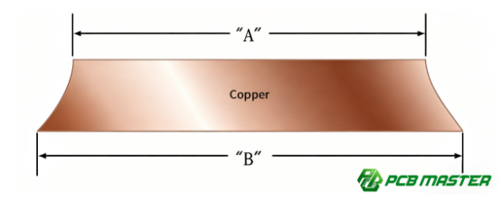
A trapezoidal shape refers to a line with edges that are sloped rather than straight, giving the line a “wider base” and a narrower top. In the context of PCB lines, this irregular shape forms during the etching process when copper traces are exposed to the etching solution. Ideally, the etching should leave a vertical, straight edge. However, due to the nature of the etching process, the solution sometimes attacks the sides of the trace, causing it to taper inward and creating a trapezoidal profile. The wider base at the bottom of the trace is due to the etching solution's ability to spread out slightly as it removes copper from the edges, especially when the protective layer does not perfectly seal the trace.
What impact does a trapezoidal edge have on PCB lines?
Trapezoidal edges can negatively affect PCB performance, especially in high-speed circuits. The irregular shape alters the signal path and can lead to increased resistance or impedance mismatches. This can distort signals, causing errors or data loss, particularly in RF (radio frequency) and high-frequency digital applications. Additionally, these irregular edges reduce the effective cross-sectional area of the trace, which can limit the amount of current the trace can carry without overheating. If the trapezoidal effect is severe, it can even cause short circuits if two adjacent traces are too close. Thus, maintaining straight, vertical edges is critical for high-performance PCBs.
How Does Side-Etching in the Etching Process Lead to Trapezoidal Shapes?
Side-etching in the etching process leads to trapezoidal shapes because the etching solution not only removes copper directly beneath the resist but also etches the sides of the trace, creating sloped, tapered edges instead of vertical ones.
Overview of the Etching Process
The etching process is a key step in creating PCB traces. It involves several stages:
1. Lamination: A layer of photoresist material (dry film or liquid) is applied to the copper-clad board.
2. Exposure: The board is exposed to ultraviolet (UV) light through a mask containing the circuit design. The exposed areas of the photoresist undergo a chemical change.
3. Development: The exposed photoresist is washed away, leaving behind the areas that need to be etched (the copper traces).
4. Etching: The board is immersed in an etching solution, usually a strong acid or alkaline mixture, which removes the exposed copper areas, leaving only the desired copper traces.
5. Stripping: The remaining photoresist is removed, leaving behind the finished PCB with its copper traces.
This process is crucial for defining the circuit layout, but it is during the etching stage that side-etching occurs, causing the trapezoidal shape.
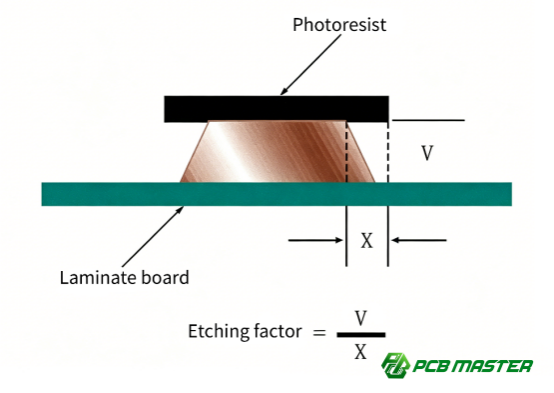
Definition and Mechanism of Side-Etching
Side-etching happens when the etching solution not only attacks the copper directly under the photoresist but also eats away at the copper along the sides of the resist. Ideally, the etching solution should only remove copper directly beneath the resist, leaving perfectly vertical edges. However, in reality, the solution can spread out slightly, causing the copper to be etched from the sides, which results in sloped, trapezoidal edges.
Ideal vs. Actual Etching Effects
In an ideal etching process, the copper should be etched away vertically, leaving straight, uniform edges. However, due to the physical nature of the etching solution and its interaction with the resist, some of the liquid creeps under the resist's edge and etches the sides of the trace. This leads to irregular, tapered shapes rather than sharp, straight lines.
Impact of Side-Etching on Trapezoidal Shapes
The amount of side-etching (referred to as "side-etch depth") directly influences the appearance of the copper trace. The more the etching liquid spreads sideways, the greater the side-etch depth, and the more pronounced the trapezoidal shape becomes. Even a small amount of side-etching can cause visible tapering at the edges, affecting both the physical appearance and electrical performance of the PCB. In high-precision applications, this can lead to issues like signal distortion or reduced current-carrying capacity.
Key Factors Affecting Trapezoidal PCB Edges
Key factors affecting trapezoidal PCB edges include the etching method, type and condition of the etching solution, copper foil thickness, and the quality of the resist layer, all of which influence side-etching and edge precision.
How Does the Etching Method Affect PCB Edge Shape?
The type of etching method used plays a significant role in how trapezoidal edges form. There are two main types of etching methods: immersion (dipping) etching and spray etching.
l Immersion Etching: In this method, the entire PCB is submerged in an etching solution. This method tends to result in more significant side-etching, leading to rougher, less precise edges and an increased risk of trapezoidal shapes.
l Spray Etching: In this more modern approach, etching solution is sprayed onto the PCB surface under high pressure. This method offers better control, reducing the amount of etching that occurs on the sides of the trace. Spray etching minimizes the chances of side-etching and helps create cleaner, more vertical edges. The precise control over spray angle, pressure, and uniformity can significantly reduce side-etching effects.
How Do the Type and Condition of Etching Solution Affect Side-Etching?
The etching solution’s properties play a crucial role in the etching process. There are two main types of etching solutions: acidic and alkaline.
l Acidic Etching Solution: Acid-based etching solutions tend to have a faster etching rate, which can increase the likelihood of side-etching if not controlled carefully.
l Alkaline Etching Solution: Alkaline solutions often offer more uniform etching but might take longer to etch through copper, reducing the risk of side-etching.
The concentration and temperature of the etching solution also matter. Higher concentration and warmer temperatures can cause the etching solution to react more aggressively, increasing side-etching and leading to more pronounced trapezoidal edges. Older etching solutions, which have lower concentrations of active chemicals, can lead to uneven etching, further exacerbating side-etching.
What is the Relationship Between Copper Foil Thickness and Etching Results?
The thickness of the copper foil on the PCB affects how the etching process works. Thicker copper foil requires longer etching times to remove the same amount of copper, which gives the etching solution more time to spread under the photoresist, increasing side-etching and resulting in more trapezoidal edges.
l Thin Copper Foil: To minimize this, thin copper foil is often used for fine-pitch or high-precision PCB designs. Thin copper etches more quickly and evenly, reducing the likelihood of side-etching and leading to cleaner, more accurate edges. This is why thinner copper is preferred in applications requiring detailed traces, like high-frequency circuits.
How Does the Quality of the Resist Layer Impact Side-Etching?
The quality of the photoresist layer (such as dry film resist) has a direct impact on the amount of side-etching. A stronger bond between the resist and copper surface helps prevent the etching solution from creeping under the resist, reducing side-etching. If the resist is too thick or poorly adhered, it may allow more etching solution to leak under the resist, causing more pronounced side-etching and trapezoidal edges.
Additionally, resist resolution is important. Higher resolution allows for finer details, but thicker resist layers can create “roof-like” overhangs that give the etching solution more space to attack the edges, increasing side-etching.
By improving the quality and adhesion of the resist layer, manufacturers can significantly reduce side-etching and improve the overall quality of PCB traces.
How to Control Trapezoidal PCB Edges?
Trapezoidal PCB edges can be controlled by optimizing etching parameters, maintaining equipment for precise spray control, and selecting high-quality materials and etching solutions that minimize side-etching.
Optimizing Etching Parameters
To minimize trapezoidal edges, it’s essential to optimize the etching parameters, including the etching solution concentration, temperature, and spray method. Adjusting the etching solution concentration ensures the solution reacts at an optimal rate, reducing uneven etching. Higher temperatures can speed up the etching process but might increase side-etching, so controlling the temperature helps maintain consistency. Spray etching, as opposed to immersion etching, is a more controlled method that limits side-etching. It allows the etching liquid to hit the PCB at specific angles and pressures, reducing the amount of solution that spreads under the resist and preventing unwanted sloped edges.
It’s also important to control etching time. Over-etching, or letting the PCB sit in the etching solution for too long, leads to deeper side-etching, creating more noticeable trapezoidal shapes. By precisely timing the etching process, you can ensure that the edges remain as vertical as possible.
Maintaining Etching Equipment
Regular cleaning and maintenance of etching equipment is crucial to ensure stable operation. Over time, equipment can accumulate residues or degrade, causing irregular spraying or uneven solution distribution. Keeping the spray nozzles and etching chambers clean ensures that the etching solution is applied evenly, reducing side-etching.
Additionally, precise control of the spray angle and pressure is necessary. If the spray is too intense or at an incorrect angle, it can lead to inconsistent etching, increasing the risk of side-etching. Modern etching systems often come with features that allow for adjustable spray angles and pressure settings, enabling manufacturers to fine-tune the process for optimal edge quality.
Choosing the Right Materials and Etching Solution
Selecting the appropriate copper foil and resist materials is another key factor in controlling trapezoidal edges. High-quality copper foil with a consistent thickness is easier to etch uniformly, reducing the chances of uneven side-etching. Similarly, the resist material must adhere well to the copper surface to prevent the etching solution from creeping underneath and causing sloped edges. Using resists with good adhesion properties ensures that the copper is well-protected during etching, minimizing unwanted side-etching.
Choosing the right etching solution is equally important. Different applications may require different etching solutions:
l Acidic etching solutions are faster and more aggressive but need careful monitoring to avoid excessive side-etching.
l Alkaline etching solutions provide a more controlled etching process and are ideal for delicate or high-precision PCB designs.
By choosing the right materials and etching solution for each application, manufacturers can reduce the risk of side-etching and maintain clean, precise PCB traces.
How Do Trapezoidal Edges Affect PCB Design and Performance?
Trapezoidal edges in PCB traces can lead to impedance mismatches, signal distortion, reduced current-carrying capacity, and increased risk of short circuits, especially in fine-line designs.
Signal Integrity and Impedance Control
Trapezoidal edges can significantly impact signal integrity and impedance matching in PCBs. Impedance refers to the resistance of a trace to the flow of an electrical signal. Ideally, the PCB traces should have clean, vertical edges to maintain a consistent impedance along the entire trace. When the edges are trapezoidal, the shape of the trace becomes irregular, causing impedance to fluctuate along the line. This results in signal reflection, distortion, and potential data loss, especially in high-frequency circuits.
In high-frequency circuit design, where signal integrity is crucial, the trapezoidal edges can cause signal reflections due to impedance mismatches. To compensate for this, designers often model the effects of trapezoidal edges and adjust the trace width or use specific trace routing techniques to reduce these distortions. Techniques like controlled impedance traces and buffering are employed to mitigate the negative effects of these edge irregularities.
Current Carrying Capacity
Trapezoidal edges can also affect a PCB's ability to carry electrical current. The effective cross-sectional area of a trace is reduced when its edges are not perfectly vertical. This reduces the amount of current the trace can carry without overheating. The more severe the trapezoidal effect, the smaller the effective cross-section, meaning that the trace may overheat or fail if it carries too much current.
Factors like copper thickness and trace width can influence how well the trace handles current. Thicker traces typically carry more current, but if side-etching reduces their width, they may no longer carry the expected load. To prevent overheating or failures, designers must ensure that traces are wide enough to handle the required current even if there is slight side-etching.
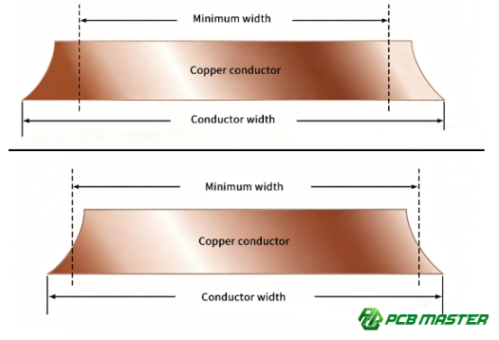
Challenges in Fine Line Processing
Fine line processing is especially sensitive to trapezoidal edges. As the trace width becomes smaller, even small irregularities in the edge can cause short-circuit risks. In extreme cases, adjacent traces can short-circuit due to excessive side-etching, especially if the traces are routed too close together.
For precision PCBs, the limitations of fine line processing become evident when the line spacing is reduced to very small widths. In such cases, even minimal side-etching can cause connection between traces, leading to short circuits or signal cross-talk. This makes it difficult to achieve high-density designs without careful control of the etching process and tight design rules.
To overcome these challenges, designers must ensure strict control over the etching parameters and adhere to specific design guidelines, such as trace width and spacing limits, to reduce the risk of short circuits and other defects.
How to Reduce Trapezoidal Edges in PCB Manufacturing?
Industry Best Practices
To minimize trapezoidal edges, leading PCB manufacturers focus on controlling side-etching through optimized etching processes. One common approach is to use spray etching rather than immersion etching. Spray etching provides more precise control over the etching liquid, reducing the chance of side-etching that causes sloped edges. Additionally, manufacturers carefully control etching solution concentration and temperature to ensure a balanced etching rate, avoiding over-etching that could lead to undesirable trace shapes.
To further reduce side-etching, some manufacturers use advanced masking techniques, ensuring that the photoresist layer adheres strongly to the copper surface. Strong adhesion prevents the etching solution from creeping under the resist and forming sloped edges. Regular equipment maintenance and careful calibration also play a crucial role, as well-maintained machines deliver more consistent etching results.
Process Control and Technological Advancements
Recent technological advances have significantly improved PCB etching quality. One such innovation is laser direct imaging (LDI), which allows for higher precision in defining PCB traces and reducing the risk of side-etching. LDI uses lasers to directly write the circuit patterns, eliminating some of the issues associated with traditional photolithography.
In precision manufacturing, the introduction of higher-resolution photoresists and automated etching systems allows for finer control over trace definition. These systems ensure that etching solutions are applied uniformly, minimizing the risk of trapezoidal shapes. Moreover, the development of high-precision etching equipment with features like adjustable spray angles and pressure offers even more control, improving the overall quality of PCB traces and reducing side-etching.
By implementing these best practices and adopting new technologies, PCB manufacturers can significantly reduce trapezoidal edge formation, ensuring more reliable and precise circuit boards for various applications.
Conclusion
Managing trapezoidal edges in PCB manufacturing is crucial for ensuring the reliability and performance of your circuits. By optimizing etching parameters, maintaining equipment, and leveraging advanced technologies, manufacturers can minimize the impact of side-etching and produce high-quality PCBs that meet the demands of modern electronics. Whether you're working on high-frequency designs, power circuits, or precision applications, reducing these edge irregularities helps maintain signal integrity, current-carrying capacity, and overall circuit functionality.
For companies looking to ensure precision and quality in their PCB production, PCBMASTER stands as a trusted partner. As an experienced PCB and PCBA supplier, PCBMASTER is committed to delivering high-quality, reliable products that meet the highest industry standards. With cutting-edge manufacturing processes and a focus on precision, PCBMASTER helps businesses achieve the optimal performance they require in every PCB design.
FAQs
Why Do My PCB Lines Have Sawtooth or Irregular Shapes?
This phenomenon is usually caused by the side-etching effect during the etching process. When the PCB is submerged in the etching solution, the solution doesn't just etch the copper directly under the resist layer; it also spreads to the sides of the copper trace. This sideward etching removes copper from the trace edges, creating a sawtooth pattern or irregular shapes. Ideally, the etching should be vertical to create straight lines, but side-etching causes the edges to taper inwards, leading to a trapezoidal or irregular profile.
How Can I Improve Side-Etching in PCB Lines?
To reduce the side-etching effect, several factors must be optimized during the etching process:
l Etching solution concentration: Too concentrated a solution can lead to aggressive etching, increasing side-etching. Lowering the concentration can reduce this effect.
l Temperature control: High temperatures can speed up the etching process, but they also increase side-etching. Maintaining an optimal temperature is key.
l Spray method: Switching from immersion to spray etching allows for more precise application of the etching solution, reducing the spread of the solution to the sides.
l Copper foil and resist material selection: Choosing high-quality copper foil with consistent thickness and strong resist adhesion can help minimize the risk of side-etching, as they prevent the etching solution from creeping under the resist layer.
Does Trapezoidal PCB Line Shape Affect Circuit Performance?
Yes, trapezoidal shapes can significantly affect the performance of your PCB, especially in high-frequency circuits and fine-line designs. The irregular edges can lead to impedance mismatches, causing signal distortion and signal reflection, which in turn may result in data loss or errors. Additionally, the reduced cross-sectional area of a trace due to side-etching lowers its current-carrying capacity, which can cause overheating or even failure in circuits designed to handle higher currents.
How Do I Choose the Right Etching Solution to Reduce Trapezoidal Edges?
To minimize trapezoidal edges, it's crucial to choose the appropriate etching solution. There are two main types of etching solutions:
l Acidic etching solutions tend to be faster but can cause more side-etching if not controlled carefully.
l Alkaline etching solutions generally offer better control and more uniform etching, making them ideal for reducing side-etching and achieving cleaner, sharper edges.
Maintaining proper concentration and solution freshness is essential to ensure the etching solution works effectively without causing excessive side-etching. Regularly replacing the etching solution and keeping it within the recommended concentration range helps ensure consistent results.
Why Are Fine Lines More Susceptible to Trapezoidal Edges?
Fine-line designs are particularly vulnerable to trapezoidal edges because their narrow width makes them more sensitive to side-etching. In fine-line PCBs, even a small amount of side-etching can significantly alter the trace shape. Additionally, if the copper foil is thicker, the etching solution has more time to attack the sides of the trace, increasing the likelihood of side-etching and leading to a more pronounced trapezoidal shape. Therefore, for fine-line PCBs, manufacturers often use thinner copper foil to reduce etching time and minimize side-etching.
Author Bio
Hi, I'm Carol, the Overseas Marketing Manager at PCBMASTER, where I focus on expanding international markets and researching PCB and PCBA solutions. Since 2020, I've been deeply involved in helping our company collaborate with global clients, addressing their technical and production needs in the PCB and PCBA sectors. Over these years, I've gained extensive experience and developed a deeper understanding of industry trends, challenges, and technological innovations.
Outside of work, I'm passionate about writing and enjoy sharing industry insights, market developments, and practical tips through my blog. I hope my posts can help you better understand the PCB and PCBA industries and maybe even offer some valuable takeaways. Of course, if you have any thoughts or questions, feel free to leave a comment below—I'd love to hear from you and discuss further!

