


How 3D Printing Is Revolutionizing PCB Design: Benefits and Innovations
PCB design is undergoing a transformation thanks to 3D printing. Traditional manufacturing methods often involve long lead times and high costs, but 3D printing offers faster prototyping, increased customization, and more efficient production. This innovation is not only speeding up design processes but also enabling new possibilities in electronics across various industries. In this article, we’ll dive into how 3D printing is revolutionizing PCB design, its benefits, and the cutting-edge innovations reshaping the field.
Understanding PCB Design and the Impact of 3D Printing on Its Evolution
PCB design involves creating the layout for circuit boards that connect and support electronic components, and 3D printing is revolutionizing this process by enabling faster, more flexible, and cost-effective prototyping and production.
Overview of PCB Design
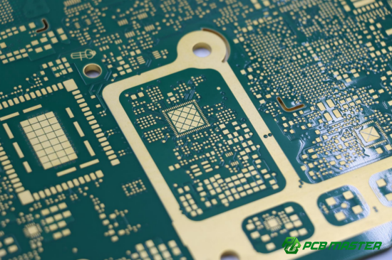
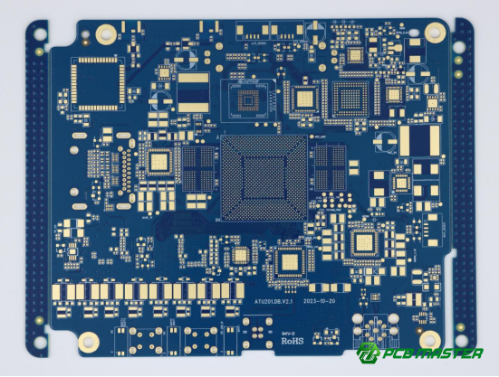
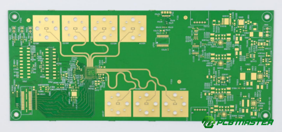
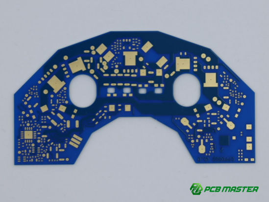
PCB design refers to the process of creating the layout for a printed circuit board, which is the foundation of almost all electronic devices. A PCB serves as the physical platform that connects and supports electrical components, such as resistors, capacitors, and microchips, through conductive pathways. These pathways, or traces, are usually made of copper, and they allow electrical signals to flow between components, ensuring that the device functions as intended.
PCBs are crucial in electronics because they provide both mechanical support and electrical connections in a compact and organized manner. Without PCBs, it would be difficult to build reliable and efficient electronic systems. They are used in everything from smartphones to medical devices, making them an essential element of modern technology.
Introduction to 3D Printing in PCB Design
The Role of 3D Printing in PCB Design:
3D printing is rapidly transforming how PCBs are designed and manufactured. Traditionally, producing PCBs involved time-consuming processes such as etching copper layers onto a rigid board. However, 3D printing allows engineers to create complex PCB prototypes faster, with fewer materials, and at lower costs.
With 3D printing, it’s possible to print entire PCBs with embedded components, flexible structures, and multi-material layers, which would have been difficult or impossible to achieve using traditional methods. This technology also makes it easier to quickly iterate and test designs, reducing the overall time to market for new electronic products. As a result, 3D printing is enabling more innovation in PCB design, particularly in industries that require customized or highly complex circuit boards.
The Evolution of PCB Manufacturing
Background on Traditional PCB Manufacturing Methods:
Traditionally, PCB manufacturing involves several intricate steps. First, a design is created on a computer, then transferred to a copper-clad board. The copper layers are etched away using acid or other chemicals to leave behind the desired circuit paths. Components are then soldered onto the board, creating a final product. While these processes have been highly effective for mass production, they can be costly and slow, especially for small runs or prototype designs.
Limitations of Traditional Methods:
One of the key limitations of traditional PCB manufacturing is its reliance on rigid, fixed processes. For example, creating custom shapes or highly complex multi-layer designs is difficult and expensive. Additionally, prototyping with traditional methods can take weeks due to the need for tooling and testing. These challenges can delay innovation and increase costs, particularly for industries that require rapid iteration of designs.
As a result, designers and engineers are increasingly turning to 3D printing for faster, more flexible, and cost-effective PCB prototyping and production.
Key differences between 3D Printing in PCB Design and Traditional Methods:
| Feature | 3D Printing in PCB Design | Traditional Methods |
| Prototyping Speed | Fast and efficient; allows rapid iterations and adjustments. | Slower due to the need for tooling, etching, and multiple steps. |
| Cost | Cost-effective for small batches and prototypes. | Expensive, especially for small runs due to tooling and setup costs. |
| Design Flexibility | Highly flexible; allows for complex, custom shapes and embedded components. | Limited flexibility; complex shapes and multi-layer designs are costly and challenging. |
| Material Options | Can use various materials including conductive resins and flexible substrates. | Limited to specific materials (typically copper and fiberglass). |
| Complexity | Capable of printing multi-material and flexible PCBs in one process. | Complex designs require multiple steps, and multi-material integration is difficult. |
| Customization | Ideal for highly customized designs, including flexible and wearable PCBs. | Customization is possible but often requires more time and higher costs. |
| Production Time | Significantly reduced production time for prototypes and small runs. | Longer production time due to various manual processes. |
| Environmental Impact | Reduces waste by using only the required materials for printing. | Produces more waste during the etching and manufacturing process. |
| Integration of Components | Allows embedding components directly within the PCB structure. | Components are added after PCB is produced, limiting integration. |
What Are the Key Benefits of 3D Printing in PCB Design?
The key benefits of 3D printing in PCB design include faster prototyping, cost-effectiveness for small batches, enhanced design flexibility, and reduced material waste, making it an efficient and sustainable solution for modern electronics.
Increased Prototyping Speed
How 3D printing accelerates the prototyping process for PCB designs:
3D printing significantly speeds up the prototyping process in PCB design by allowing quick creation of physical models directly from a digital file. Traditional PCB manufacturing methods involve many steps, including etching, drilling, and soldering, which can take days or even weeks. In contrast, 3D printing can produce a working model in hours, enabling faster testing and validation.
Time savings in producing working models:
With 3D printing, engineers can rapidly produce prototypes without waiting for physical components or expensive tools to be made. This is particularly beneficial for testing new designs, ensuring that engineers can evaluate the functionality of a design much faster than with traditional methods. For example, a smartphone company can test different PCB configurations in a matter of hours, rather than waiting for weeks for a traditional board to be created.
Speed in iterations and adjustments:
3D printing also speeds up the process of modifying designs. If changes are needed, the updated model can be printed in a fraction of the time, enabling engineers to make adjustments quickly and efficiently. This flexibility accelerates the iteration process, ultimately shortening the time to market for new electronic devices.
Cost-Effectiveness for Small Batches
How 3D printing reduces the cost of small-run PCB manufacturing:
In traditional PCB manufacturing, producing small batches or prototypes can be expensive due to the need for specialized tooling and molds. However, 3D printing eliminates the need for these costly investments. Once the digital design is created, the PCB can be printed directly, reducing overhead and setup costs.
No need for expensive molds or tooling:
Traditional PCB production requires creating etching molds, drilling tools, and other specialized equipment for each design. These tools can be expensive and time-consuming to create. With 3D printing, no such tooling is required, as the design is directly printed onto the substrate. This means that small-run and prototype production becomes far more affordable.
Reduction in material wastage:
Another cost-saving aspect of 3D printing is its ability to use only the material needed for the design. In traditional PCB manufacturing, excess material is often wasted during the etching and cutting processes. With 3D printing, material is added layer by layer, minimizing waste and reducing the overall cost of production. This is especially beneficial for small batches where material costs are proportionally higher.
Design Flexibility and Customization
How 3D printing enables more creative and customized designs that were previously difficult or impossible to achieve:
3D printing allows for the creation of PCBs with intricate and customized features that would be challenging to achieve using traditional methods. With the flexibility of 3D printing, engineers can easily incorporate complex shapes, embedded components, and multi-layered designs, making it a powerful tool for innovative PCB development.
Complex shapes, multi-layered circuits, and embedded components:
One of the biggest advantages of 3D printing in PCB design is its ability to produce complex shapes and multi-layer circuits that are not possible with traditional etching or drilling methods. For example, designers can embed components like capacitors or resistors directly within the board, saving space and improving performance. Additionally, 3D printing allows for flexible, curved, or wearable PCBs, opening up new possibilities for industries like healthcare and wearable technology.
3D printing also enables the use of different materials within a single PCB, allowing for better performance characteristics, such as enhanced conductivity or insulation where needed. This level of customization was previously impractical in traditional methods, where creating custom shapes or adding embedded components would have been labor-intensive and expensive.
Reduced Waste and Environmental Impact
How 3D printing contributes to sustainability in PCB production:
3D printing is a more sustainable method of manufacturing PCBs compared to traditional processes. Traditional PCB manufacturing involves a lot of material waste due to the etching and cutting processes, where much of the copper and other materials are discarded. In contrast, 3D printing adds material only where needed, significantly reducing waste.
Comparison to traditional PCB manufacturing processes:
In traditional PCB manufacturing, excess material is often wasted during the creation of the copper traces, and toxic chemicals are used in the etching and cleaning processes. These materials can harm the environment if not disposed of properly. 3D printing, on the other hand, uses fewer materials and can even be done with more eco-friendly materials, such as biodegradable plastics or conductive resins, reducing the environmental impact.
Material efficiency in the design and production phases:
With 3D printing, engineers can precisely control how much material is used, minimizing waste throughout the design and production phases. This efficiency extends to both the material itself and the energy used in the process, making it a more sustainable choice for PCB production. For example, in the production of a flexible PCB for a wearable device, 3D printing can create the exact amount of material needed for each individual unit, reducing the need for mass production and minimizing leftover materials.
How Does 3D Printing Work in PCB Prototyping?
3D printing in PCB prototyping works by using specialized materials to layer conductive and insulating components, allowing for rapid design, printing, and testing of complex circuit boards with embedded components.
Material Selection for 3D Printed PCBs
What materials can be used in 3D printing for PCBs?
In 3D printing for PCB prototyping, a range of materials is used to create both the structural and electrical components of the board. Common materials include conductive inks, conductive resins, and non-conductive filaments.
Differences between conductive and insulating materials in PCBs:
l Conductive Materials: These materials, such as silver-based inks or copper-loaded filaments, are used to create the electrical traces on the PCB. Conductive materials are essential for forming the paths through which electrical signals flow between components, enabling the PCB to function properly.
l Insulating Materials: Non-conductive materials like plastic or specialized resins are used to separate and protect different conductive traces. These materials ensure that electrical signals don’t accidentally flow between paths where they shouldn't, preventing short circuits. For example, the base layer of a PCB is typically made from insulating material to provide structural integrity and prevent unwanted conductivity.
By carefully selecting both types of materials, engineers can create fully functional, flexible, and multi-layered PCBs suitable for various applications, including electronics, wearables, and IoT devices.
Steps Involved in 3D Printing a PCB Prototype
How does 3D printing a PCB prototype work?
1. Design Software and Modeling:
The first step in 3D printing a PCB is designing the circuit using specialized PCB design software, such as Eagle, Altium, or KiCad. These programs allow engineers to create the schematic, arrange components, and define the pathways (traces) for the electrical signals. The design is then converted into a 3D model that can be interpreted by the 3D printer.
2. Material Preparation and Printing Stages:
After the design is finalized, the required materials (conductive and non-conductive) are loaded into the 3D printer. The printer starts by laying down a base layer of non-conductive material to form the structural part of the PCB. Following that, it prints the conductive traces layer by layer using conductive ink or resin, building up the electrical pathways. Multi-material printers can combine different types of material, like insulating and conductive filaments, during the same print cycle.
3. Post-processing and Testing:
Once the PCB is printed, it undergoes post-processing, which may involve cleaning the surface, curing the materials with UV light (if applicable), and inspecting the print for defects. Afterward, electrical components such as resistors, capacitors, and microchips are soldered onto the board. Finally, testing is performed to ensure that the circuit works as expected, with checks for electrical connectivity, functionality, and performance.
Challenges in 3D Printing PCBs
What are the challenges in 3D printing PCBs?
1. Material Limitations:
While 3D printing has advanced, it still faces material challenges. Conductive inks and resins often do not provide the same level of conductivity as traditional copper traces used in conventional PCB manufacturing. This can limit the current-carrying capacity and the overall performance of the PCB, particularly in high-frequency applications. Additionally, the range of available materials for 3D printed PCBs is still narrower compared to traditional PCB production, where many more specialized materials are available.
2. Printing Precision and the Resolution Challenge:
Precision is another challenge in 3D printing PCBs. The resolution of most 3D printers, especially those used for PCB prototyping, may not be fine enough to produce highly detailed, small, or densely packed circuit traces. This can result in blurry or imprecise traces, affecting the performance of the PCB. For high-performance applications, the resolution needs to be high enough to ensure accurate trace widths and clean separation between conductive paths, which can be difficult to achieve with some consumer-grade 3D printers.
3. Integration of Electrical Components:
Integrating electrical components directly into a 3D printed PCB is another challenge. While it’s possible to embed components in the design, placing components such as microchips, capacitors, and resistors accurately during the 3D printing process requires high precision. After the printing is completed, the components often need to be soldered onto the board, which adds an extra step to the process. Additionally, the mechanical and electrical properties of 3D printed boards might not match those of traditionally manufactured PCBs, affecting their long-term reliability and performance in commercial products.
What Are the Innovations Driving 3D Printing in PCB Design?
The innovations driving 3D printing in PCB design include the integration of embedded components, the development of flexible and wearable PCBs, the use of multi-material printing for complex designs, and the emergence of self-assembling and smart PCBs for advanced functionality.
Integration of Embedded Components
How can 3D printing embed resistors, capacitors, and even microchips directly into the PCB structure?
3D printing technology has advanced to the point where components such as resistors, capacitors, and even microchips can be directly embedded into the PCB during the printing process. This eliminates the need for additional soldering and assembly of these components after the PCB is printed, streamlining the production process.
Benefits of embedded components for compact designs and increased functionality:
Embedding components directly within the PCB structure allows for more compact and efficient designs. By reducing the need for external components, the overall size of the device can be minimized, which is particularly valuable for applications where space is limited, such as wearable electronics. This also improves the performance of the circuit by reducing the number of physical connections needed, which can reduce signal interference and improve reliability. For instance, in a wearable medical device, embedding sensors directly into the PCB allows for a thinner, more comfortable design while maintaining high functionality.
Flexible and Wearable PCBs
What is the impact of 3D printing on flexible and wearable PCB designs?
3D printing has significantly influenced the development of flexible and wearable PCBs, offering unique capabilities that traditional manufacturing methods cannot. With 3D printing, it’s possible to produce PCBs that are not only lightweight but can also bend and stretch without damaging the circuit.
Applications in the medical, consumer electronics, and automotive sectors:
Flexible and wearable PCBs are increasingly used in medical devices, such as heart monitors or fitness trackers, where the PCB needs to conform to the body’s contours. In consumer electronics, flexible PCBs enable more compact, lightweight devices like smartphones or foldable displays. The automotive industry also benefits from flexible PCBs in applications such as sensors or flexible displays within vehicles. These applications showcase how 3D printing is expanding the possibilities of PCB design, enabling products that were once unfeasible with traditional methods.
Multi-material Printing
How is multi-material 3D printing enabling more sophisticated PCBs?
Multi-material 3D printing allows for the combination of different types of materials within a single print, such as conductive and non-conductive materials, in a seamless process. This enables the creation of more complex PCBs with improved functionality and performance.
Combining conductive and non-conductive materials in a single print:
By printing conductive materials (like silver or copper ink) alongside insulating materials (like plastic or resin), multi-material printing simplifies the process of creating complex, functional PCBs. For example, a single 3D printed PCB can include the necessary conductive traces for electricity, along with the insulating layers that protect and separate different traces. This reduces the need for additional processing steps, allowing for faster production times and a more efficient design.
Impact on multi-layer PCB designs:
Multi-material 3D printing also supports the creation of multi-layer PCBs, where each layer serves a specific function, such as routing power or handling high-frequency signals. This opens the door for more sophisticated designs, including those used in advanced electronics like smartphones, wearables, or IoT devices. The ability to print multiple materials in a single pass helps reduce complexity and increases design flexibility.
Self-assembling and Smart PCBs
What are self-assembling and smart PCBs?
Self-assembling PCBs are a futuristic concept enabled by 3D printing, where the PCB can automatically arrange or assemble itself once printed. Smart PCBs, on the other hand, are PCBs that integrate intelligence and adapt to changes in their environment or functionality over time. These innovations push the boundaries of what’s possible in electronics, combining physical and digital worlds in new ways.
Potential applications in robotics and AI:
Self-assembling PCBs could have significant applications in robotics, where components can automatically organize themselves into a functional circuit after being printed. This could reduce labor costs and time in assembly processes. Smart PCBs, which could adjust their functions based on environmental inputs or sensor data, have the potential to revolutionize AI applications. For instance, a smart PCB in a robotic arm could adjust its behavior based on feedback from its environment, leading to more responsive and adaptive robotic systems. These types of innovations in PCB design are expected to play a key role in the future of advanced technologies, including AI, robotics, and autonomous systems.
How Is 3D Printing Enhancing PCB Testing and Iteration?
3D printing enhances PCB testing and iteration by enabling rapid prototyping, faster testing of design changes, and more cost-effective modifications, allowing engineers to quickly refine designs and test them under real-world conditions.
Rapid Testing with 3D Printed Prototypes
How does 3D printing allow engineers to test design functionality faster than traditional methods?
3D printing enables rapid testing of PCB prototypes by quickly producing physical models directly from digital designs. This accelerates the process of testing different configurations, as engineers can test multiple iterations within hours or days, compared to the weeks it might take using traditional PCB manufacturing.
Real-time testing of different PCB configurations:
With 3D printing, engineers can quickly modify the design and print a new prototype to test different configurations. For example, if an engineer wants to test a change in the layout of a circuit, they can immediately print a new version and run tests to see how the modification affects the performance. This rapid testing allows engineers to find the optimal design faster and more efficiently, leading to improved products and shortened development cycles.
Reducing Iteration Time and Costs
How does 3D printing accelerate the feedback loop and reduce the need for traditional PCB manufacturing?
Traditional PCB manufacturing requires several steps, including creating prototypes, etching, and testing, all of which can be costly and time-consuming. With 3D printing, engineers can skip many of these steps and quickly produce prototypes in-house, making it easier and faster to iterate on designs.
Cost and time savings when modifying prototypes and design changes:
3D printing reduces both the time and cost involved in modifying PCB prototypes. If an engineer needs to make a small adjustment to the design, they can simply update the digital file and print a new version—without waiting for new molds, etching processes, or other costly steps associated with traditional methods. This not only saves time but also reduces costs, especially for small batches or prototype runs, making 3D printing an economical choice for iterative design processes.
Advanced Circuit Simulation
How does 3D printing allow for testing in different real-world conditions with more flexible and varied designs?
3D printing makes it possible to test PCBs in a variety of real-world conditions by offering greater flexibility in design. Engineers can create prototypes that simulate the exact environmental factors the final product will face, such as bending, stretching, or exposure to heat. This level of flexibility is difficult to achieve with traditional manufacturing techniques.
Testing in flexible and varied designs:
For example, engineers can use 3D printing to create flexible PCBs that are designed for wearables or devices exposed to movement and pressure. Traditional PCB testing would be limited to rigid designs, but 3D printing allows engineers to test how a flexible PCB behaves under real-life conditions. This results in more accurate, reliable testing that helps improve product durability and functionality. Furthermore, 3D printing allows for a broader range of materials to be used in testing, providing better insights into how different materials perform under specific conditions.
What Are the Future Trends of 3D Printing in PCB Design?
The future trends of 3D printing in PCB design include advances in conductive inks and hybrid materials, the integration of AI and machine learning for optimized design and error detection, and the widespread adoption of 3D printing for low-volume and high-complexity PCB production.
Advances in Materials for 3D Printed PCBs
What are the upcoming developments in materials for 3D printing in PCB design?
The future of 3D printing in PCB design is closely tied to advancements in materials. As technology progresses, new materials are being developed that enhance the functionality and performance of 3D printed PCBs. These materials include conductive inks and resins as well as hybrid materials that combine both electrical and mechanical properties.
Conductive inks and resins:
Currently, most 3D printed PCBs use conductive inks (like silver or copper-based inks) to create the necessary electrical traces. As materials science advances, new types of conductive inks and resins with better conductivity, durability, and flexibility are being developed. These materials will allow for faster, more reliable designs and enable the production of more advanced PCBs that can carry higher currents and operate at faster speeds, meeting the growing demands of modern electronics.
Hybrid materials combining electrical and mechanical properties:
Another exciting development is hybrid materials that combine both electrical conductivity and mechanical strength in one material. These materials could enable the creation of PCBs that are not only electrically efficient but also strong, flexible, and heat-resistant. This would be especially useful in industries like automotive or wearables, where both electrical and physical properties are critical for performance. For instance, in flexible PCBs used in wearable devices, hybrid materials could provide the necessary conductivity while maintaining flexibility and durability under stress.
Integration of AI and Machine Learning with 3D Printing
How will AI and machine learning optimize PCB design and 3D printing processes?
The integration of AI and machine learning (ML) with 3D printing is set to revolutionize the way PCBs are designed and printed. These technologies can optimize the design process, predict performance, and detect potential errors, all of which improve the overall efficiency and reliability of PCB production.
Predictive design and automated error detection:
AI can analyze vast amounts of data from previous designs and simulations to predict the best design configurations for PCBs. This will allow for predictive design, where AI helps engineers create designs that are more likely to succeed on the first try, reducing time and costs. Additionally, ML algorithms can automate error detection during the design and printing processes, identifying issues like weak traces or areas of potential failure before the PCB is printed. This reduces the likelihood of defects and ensures a higher-quality final product.
For example, a machine learning system could identify patterns in past PCB failures and suggest design modifications, ensuring that future designs are more resilient. This would not only speed up the design process but also ensure that PCBs are more reliable and cost-effective.
Commercialization and Widespread Adoption
What is the future of 3D printing in mainstream PCB manufacturing?
As 3D printing technology continues to improve, its adoption in mainstream PCB manufacturing is expected to grow significantly. More companies will begin to use 3D printing for producing low-volume and high-complexity PCBs, which are often challenging and expensive to produce with traditional methods.
How more companies will adopt 3D printing for low-volume and high-complexity PCBs:
3D printing is particularly advantageous for low-volume production runs where traditional methods like etching and molding would be too costly. For example, startups and small businesses can use 3D printing to produce small batches of highly specialized PCBs without the large upfront costs of traditional manufacturing. This enables innovation and experimentation without the financial risks associated with mass production.
Additionally, high-complexity PCBs—such as those used in medical devices, aerospace, and wearable technology—often require intricate designs that are difficult or expensive to produce with conventional techniques. 3D printing allows these complex designs to be created more easily and affordably. As the technology advances, it is likely that 3D printing will become more widespread across various industries, offering greater flexibility, cost savings, and faster time-to-market for PCB production.
Conclusion
3D printing is revolutionizing the PCB design process, offering faster prototyping, more flexibility, and cost-effective production for complex, low-volume projects. With innovations in materials, AI integration, and widespread adoption, the future of PCB manufacturing is bright. Companies like PCBMASTER, with their expertise in PCB and PCBA solutions, are at the forefront of this transformation. As a trusted supplier, PCBMASTER is committed to providing high-quality products that meet the evolving demands of modern electronics, ensuring your designs are not only efficient but also cutting-edge. Whether you’re looking for advanced PCB prototypes or complete assembly solutions, PCBMASTER offers reliable, innovative, and high-performance products for your next project.
FAQs
1. What materials are used in 3D printed PCBs?
Explanation of materials used for 3D printing PCBs:
3D printed PCBs use a variety of materials to create the necessary electrical and structural components. These materials include conductive inks, resins, and filaments that can be used to print both the functional circuit traces and the insulating layers of the PCB.
l Conductive Resins and Inks: These are the key materials for creating the electrical pathways (traces) in 3D printed PCBs. Silver-based inks or copper-based conductive resins are commonly used due to their high conductivity, allowing for the transmission of electrical signals through the PCB. Conductive inks are used to print the circuit traces that connect various components on the board.
l Non-conductive Resins: These are used to form the insulating layers that separate the conductive traces. Non-conductive resins are often used for the substrate or base layer, and they ensure that electrical signals don't leak or cause shorts between different conductive paths.
l Hybrid Materials: Some advanced 3D printing technologies use hybrid materials that combine both conductive and insulating properties in a single material. These hybrid materials are beneficial for creating multi-layer PCBs and more complex designs, offering flexibility while maintaining performance.
2. How does 3D printing reduce the cost of PCB design?
Cost benefits of 3D printing in terms of prototyping, tooling, and material waste reduction:
l Prototyping: One of the biggest cost advantages of 3D printing in PCB design is the ability to quickly create prototypes without the need for expensive molds or tooling. Traditional PCB manufacturing requires creating molds and etching copper layers, which can be costly and time-consuming, especially for small runs or prototype batches. With 3D printing, the design is simply printed layer by layer, reducing the cost and lead time for producing prototypes.
l Tooling Costs: Traditional PCB manufacturing often requires specialized equipment, such as etching machines and drilling tools, which can be expensive and time-consuming to set up. 3D printing eliminates the need for these tools, as the printer directly builds the PCB from the digital file. This makes it more affordable for small businesses or startups to produce low-volume runs of custom PCBs.
l Material Waste Reduction: In traditional PCB manufacturing, excess material is often wasted during the etching process, where copper is removed to create circuit traces. 3D printing, however, only uses the necessary amount of material to build the PCB, which significantly reduces material waste and lowers the overall production cost.
3. What challenges are associated with 3D printing PCBs?
Current challenges in 3D printing PCBs:
l Material Limitations: Although 3D printing for PCBs has made significant strides, there are still material limitations. Current conductive materials, like conductive inks, may not provide the same level of conductivity as traditional copper used in conventional PCBs. This limits their use in high-power or high-frequency applications, where traditional materials would perform better. Additionally, the range of available materials for 3D printing is still narrower compared to traditional PCB manufacturing.
l Resolution and Precision: The resolution of 3D printers, especially those used for PCB prototyping, may not be high enough for fine-pitch designs or extremely small components. This can lead to imprecise traces and poor quality when trying to create dense or highly detailed circuits, which are often required in advanced electronics like smartphones or IoT devices.
l Electrical Conductivity: Even with conductive inks and materials, the electrical performance of 3D printed PCBs may not match the capabilities of traditional copper traces. For instance, conductive inks may not carry as much current or may have higher resistance, leading to potential issues in performance, especially in high-power applications.
4. Can 3D printed PCBs be used in mass production?
Scalability of 3D printed PCBs for large-scale production:
While 3D printing offers a significant advantage for prototyping and small-batch PCB production, it currently faces challenges when it comes to mass production. Traditional methods like etching and laminating are still more efficient for producing large volumes of PCBs due to their speed and precision. 3D printing is slower than traditional PCB manufacturing techniques, and scaling up for large production runs could become cost-prohibitive due to the time and material requirements.
However, as 3D printing technology evolves and new high-speed 3D printers are developed, it may become more feasible for high-volume production, especially for specialized or highly complex PCBs. In the future, hybrid manufacturing methods—where 3D printing is used in conjunction with traditional techniques—could allow for cost-effective mass production of certain types of PCBs, such as flexible or custom boards used in emerging technologies like wearables or IoT devices.
5. How does 3D printing improve the PCB prototyping process?
Benefits of faster iterations and testing using 3D printed PCB prototypes:
l Faster Iterations: One of the most significant benefits of 3D printing for PCB prototyping is the speed at which design iterations can be tested. With traditional methods, making a change to a PCB design typically requires new tooling and a lengthy production process. With 3D printing, engineers can quickly modify their designs and print new prototypes within hours or days, allowing for rapid iterations and faster testing.
l Testing and Validation: 3D printed prototypes make it easy to test new PCB designs in real-world conditions before committing to mass production. Engineers can quickly prototype various configurations, test different material combinations, and validate functionality, all within a much shorter time frame compared to traditional methods. This allows for faster design cycles and more efficient decision-making, leading to better products and a quicker time-to-market.
l Cost-effective Prototyping: The ability to rapidly produce and modify prototypes also means reduced costs in the design phase. Engineers can experiment with multiple versions of a design without the financial burden of traditional PCB manufacturing, which often requires expensive tooling and material waste. This cost-saving aspect is particularly useful for startups or companies working with limited resources.
Author Bio
Hi, I'm Carol, the Overseas Marketing Manager at PCBMASTER, where I focus on expanding international markets and researching PCB and PCBA solutions. Since 2020, I've been deeply involved in helping our company collaborate with global clients, addressing their technical and production needs in the PCB and PCBA sectors. Over these years, I've gained extensive experience and developed a deeper understanding of industry trends, challenges, and technological innovations.
Outside of work, I'm passionate about writing and enjoy sharing industry insights, market developments, and practical tips through my blog. I hope my posts can help you better understand the PCB and PCBA industries and maybe even offer some valuable takeaways. Of course, if you have any thoughts or questions, feel free to leave a comment below—I'd love to hear from you and discuss further!

